Efficiency droop improvement in GaN-based light-emitting diodes by
graded-composition electron blocking layer
C.H. Wang, S. P. Chang, W. T. Chang, J. C. Li, H. C. Kuo, T. C. Lu, S. C. Wang
Department of Photonics and Institute of Electro-Optical Engineering,
National Chiao Tung University, Hsinchu 30010, Taiwan
ABSTRACT
A graded-composition electron blocking layer (GEBL) with aluminum composition increasing along [0001] direction was designed for c-plane GaN-based light-emitting diodes (LEDs). The simulation results demonstrated that such GEBL can effectively enhance the capability of hole transportation across the EBL as well as the electron confinement. Consequently, the LED with GEBL grown by metal-organic chemical vapor deposition exhibited better electrical characteristics, and much higher output power at high current density, as compared to conventional LED. Meanwhile, the efficiency droop was reduced from 34% in conventional LED to only 4% from the maximum value at low injection current to 200 A/cm2.
Keywords: light-emitting diodes, efficiency droop, electron blocking layer
1. INTRODUCTION
Solid-state lighting offers much potential to save energy and to enhance the quality of our building environments, especially refers to GaN-based light emitting diodes (LEDs) [1]. GaN-based LEDs have been developed in various applications due to its widely tunable wavelength from ultraviolet to blue/green. Nevertheless, the most expected application, solid-state lighting, is still under developing, which means the state-of-the-art InGaN/GaN LEDs should be further improved. Although the light-extraction efficiency has been significantly improved by different techniques, the internal quantum efficiency (IQE) still suffers a major obstacle, i.e., the substantial decrease in efficiency with increasing injection current [2]. This efficiency droop behavior strongly limits the development of many specific applications which require the operation current of the InGaN/GaN LEDs under high injection levels. Several possible physical mechanisms leading to efficiency droop have been proposed, including carrier leakage from the active region [3], carrier delocalization [4], and Auger recombination [5].
Carrier overflow out of the active region as well as inefficient injection and transportation of holes have been identified to be the major reasons of efficiency droop [6]. To reduce the carrier overflow, an AlxGa1-xN electron blocking layer (EBL) was adopted in common LED structures. However, it has been reported that the large polarization field in AlxGa1-xN EBL reduces the effective barrier height for electrons [7]. Therefore, the carrier overflow can not be suppressed effectively. On the other hand, the polarization-field induced band bending and the valance band offset (△ Ev) at the interfaces of GaN and EBL are considered to retard the injection of holes [2, 7]. To reduce the polarization field in EBL, the polarization matched EBLs (AlInN or AlInGaN) were proposed and demonstrated to be more effective in electron confinement [8, 9]. However, it has difficulties of realization in epitaxy and the crystal quality of subsequent p-GaN layer will be degraded. Most importantly, the hole injection can not be improved effectively due to existing of the △ Ev between the last GaN barrier and the EBL [7].
2. GRADED-COMPOSITION ELECTRON BLOCKING LAYER
In this paper, we designed a graded-composition EBL (GEBL) for InGaN/GaN LEDs employing the concept of band-engineering, which not only suppressed the electron overflow out of active region, but also enhanced the hole injection. The improvements in electron confinement and hole injection of LED with GEBL were demonstrated in simulation. Then it was realized by using metal-organic chemical vapor deposition (MOCVD), and the efficiency droop in LED with GEBL was found to be much smaller than that in conventional LED with constant-composition AlxGa1-xN
EBL.
2.1 Foreword
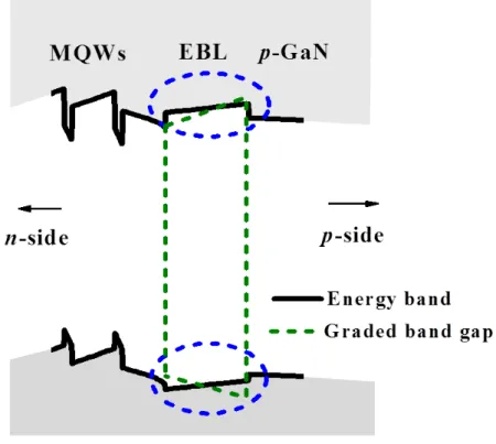
The concept of band engineering started from observation on the band diagram of InGaN/GaN LEDs. For conventional LEDs operated under forward bias, the band diagram of EBL shows triangular shape due to the internal polarization field and forward bias [10], as shown in Fig. 1. The valance band of EBL slopes upward from the n-GaN side toward p-GaN side, which retards the holes to transport across the triangular barrier. But if the composition of aluminum in EBL increases from the n-GaN side toward p-GaN side, the band-gap broadens gradually. As a result, the barrier in valance band could be level down and even overturn, while the slope of conduction band could be enhanced. Then, the improvement in capability of hole transportation across the EBL as well as the electron confinement could be expected.
Fig.1. Schematic diagram of the concept of band-engineering at EBL.
2.2 Simulation and Experiment
To check the feasibility of the hypothesis above, the band diagrams and carrier distributions in LED with GEBL were investigated firstly by APSYS simulation program. The simulation LED structures were composed of 4-μm-thick n-type GaN layer (n-doping=2×1018 cm-3), six pairs of In
0.15Ga0.85N/GaN multiple-quantum wells (MQWs) with 2.5-nm-thick wells and 10-nm-thick barriers, 20-nm-thick p-AlxGa1-xN EBL or GEBL (p-doping=5×1017 cm-3), and 200-nm-thick p-type GaN layer (p-doping=1×1018 cm-3). For the LEDs with GEBL, three types of GEBLs with compositions of aluminum graded along [0001] direction from 0% to 15, 25, 35%, respectively, were simulated and denoted as LED A, B, C. And for the conventional LED, the composition of aluminum was a constant of 15%. Commonly accepted physical parameters were adopted to perform the simulations, the percentage of screening effect of 50% , the Shockley-Read-Hall recombination lifetime of 1ns, the Auger recombination coefficient in quantum wells of 2×10-30 cm6/s, respectively [11]. Other material parameters used in the simulation can be referred to ref. 12.
Figure 2 shows the energy band diagrams of LED A, B, C at current density of 100A/cm2. According to our concept of band engineering, the degree of gradation had the decisive influence on the capability of hole injection. Even with
small degree of gradation as LED A, the slope of valance band can be leveled. Then the slope starts to overturn when the composition of aluminum at p-side increases up to 25%. Moreover, it is worth noting that the △ Ev between the last GaN barrier and the EBL is diminished in all three LEDs with GEBL. Therefore, the hole injection can be improved effectively by using the GEBL. In the meantime, as the degree of gradation increased, the conduction band offset at interface of p-GaN and EBL increases as well, so does the confinement capability of electrons. But correspondingly, the △ Ev between EBL and p-GaN increases as the composition of aluminum rises, which might retard the transportation of holes. In addition, high aluminum-composition EBL is not practical for actual application due to the low acceptor-activation efficiency and the low crystal quality in epitaxy [13]. Consequently, only the LED B with aluminum graded from 0% to 25% is discussed in the following paragraph.
Fig.2. Calculated energy band diagrams of (a) Al0GaN to Al0.15Ga0.85N (b) Al0GaN to Al0.25Ga0.75N (c) Al0GaN to Al0.35Ga0.65N graded-composition
EBL at current density of 100 A/cm2.
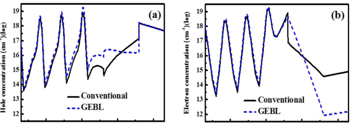
The profiles of hole and electron concentration distribution at current density of 100A/cm2 are illustrated in Fig. 3 (a) and (b), respectively. It can clearly be seen that with GEBL, injected holes uniformly distribute along the EBL region compared to conventional one, demonstrating that flat valance band indeed favored the hole transportation across EBL. Meanwhile, the hole concentration in MQWs is significantly increased as expected. Moreover, the electron concentration in MQWs is also enhanced, while the electron distribution within the GEBL region and p-GaN is enormously decreased over 2 orders. This result indicates that GEBL can suppress the electron overflow out of active region more effectively than conventional EBL, even though the conduction band offset between the last GaN barrier and the GEBL is diminished.
Fig.3. Calculated (a) hole concentration distribution (b) electron concentration distribution of conventional and GEBL LEDs at current density of 100 A/cm2.
Then, the LED structures with EBL and GEBL were grown on c-plane sapphire substrates by MOCVD. After depositing a low temperature GaN nucleation layer, a 4 μm n-type GaN layer, and ten-pair InGaN/GaN superlattice prestrain layer, the rest of the LED structures were grown basing on our simulation design. The epitaxial recipe for the GEBL is worth noting. Generally, the graded composition ternary III-Nitride semiconductors can be grown by two methods: growth temperature ramping and III/III ratio ramping [14, 15]. Here we adopted the Al/Ga ratio ramping because the temperature ramping would change the growth rate, and the higher temperature might damage the quality of QWs. The growth temperature of conventional EBL and GEBL were the same (870 ℃), and the aluminum composition profile of the GEBL was approximately graded from 0% to 25%. Finally, the LED chips were fabricated by regular chip process with ITO current spreading layer and Ni/Au contact metal, and the size of mesa is 300×300 μm2. The emission wavelengths of both LEDs were around 450 nm at 22 A/cm2.
2.3 Results and Discussion
Figure 4 shows the L-I-V curves of the conventional and GEBL LEDs. The output powers were measured with a calibrated integrating sphere. The forward voltages (Vf) at 22 A/cm2 and series resistances (Rs) of GEBL LED are 3.28 V and 7 Ω, respectively, which are lower than that of 3.4 V and 8 Ω for conventional LED. The reduced Vf and Rs can be attributed to the improvement in hole injection and the higher-efficiency p-type doping in GEBL [16]. In the case of L-I cureves in Fig. 4, although the output power of GEBL LED is a little lower at low current density (below 30 A/cm2), it increases more rapidly as increasing the injection current, as compared to the conventional one. The output power was enhanced 40% and 69% at 100 A/cm2 and 200 A/cm2, respectively. This phenomenon can be explained as following: At low current density, it is more difficult for holes to tunnel across the barrier at the interface of p-GaN and EBL in GEBL LED because the △Ev is larger than that in conventional LED. While at high current density, the tunneling process of holes can be negligible, and the diffusion process is dominated for the hole transportation into the MQW [7]. As discussion above, the diffusion process in GEBL is much easier than that in conventional one due to the flat valence band and much lower △Ev at the interface of last GaN barrier and EBL. In conjunction with the superior electron confinement, much stronger light output was achieved in GEBL LED at high current density.
Fig.4. Forward voltage and output power as a function of current density for conventional and GEBL LEDs.
Finally, the normalized efficiency of conventional and GEBL LEDs as a function of current density were investigated, as shown in Fig. 5. The maximum efficiency (ηpeak) of GEBL LED appears at injection current density of 80 A/cm2, which was much higher than that for conventional LED (at 20 A/cm2). More interestingly, the efficiency droop, defined as (ηpeak - η200 Acm-2)/ηpeak, was reduced from 34% in conventional LED to only 4% in GEBL LED. This significant improvement in efficiency can be mainly attributed to the enhancement of hole injection as well as electron confinement, especially at high current density.
Fig.5. Normalized efficiency as a function of current density for conventional and GEBL LEDs.
3. SUMMARY
In conclusion, we have designed a graded-composition electron blocking layer for InGaN/GaN LED by employing the band engineering. The simulation results showed that the triangular barrier of conventional EBL at valance band could be balanced, while the slope of conduction band could be increased by increasing the band gap of AlxGa1-xN along [0001] direction. As a result, the hole concentration in MQWs was significantly increased, while the electron distribution
within the GEBL region and p-GaN was enormously decreased over 2 orders, indicating the GEBL can effectively improve the capability of hole transportation across the EBL as well as the electron confinement. Furthermore, the LED structure with GEBL was realized by MOCVD. The L-I-V characteristics of GEBL LED showed the smaller Vf and Rs due to the improvement in hole injection and the higher-efficiency p-type doping in GEBL, as compared to the conventional LED. More importantly, the efficiency droop was reduced from 34% in conventional LED to only 4% in GEBL LED. This work implies that carrier transportation behavior could be appropriately modified by employing the concept of band engineering.
REFERENCES
[1] Department of Energy, U. S., http://www.energy.gov/
[2] M. H. Kim, M. F. Schubert, Q. Dai, J. K. Kim, E. F. Schubert, J. Piprek, Y. Park, Appl. Phys, Lett. 91, 183507 (2007).
[3] M. F. Schubert, J. Xu, J. K. Kim, E. F. Schubert, M. H. Kim, S. Yoon, S. M. Lee, C. Sone, T. Sakong, and Y. Park, Appl. Phys. Lett., 93, 041102 (2008).
[4] B. Monemar and B. E. Sernelius, Appl. Phys. Lett., vol. 91, pp. 181103 (2007). [5] A. David and M. J. Grundmann, Appl. Phys, Lett. 96, 103504 (2010).
[6] C. H. Wang, J. R. Chen, C. H. Chiu, H. C. Kuo, Y. L. Li, T. C. Lu, and S. C. Wang, IEEE Photon. Technol. Lett. 22, 236 (2010).
[7] Sang-Heon Han, Dong-Yul Lee, Sang-Jun Lee, Chu-Young Cho, Min-Ki Kwon, S. P. Lee, D. Y. Noh, Dong-Joon Kim, Yong Chun Kim, and Seong-Ju Park, Appl. Phys. Lett. 94, 231123 (2009).
[8] Suk Choi, Hee Jin Kim, Seong-Soo Kim, Jianping Liu, Jeomoh Kim, Jae-Hyun Ryou, Russell D. Dupuis, Alec M. Fischer, and Fernando A. Ponce, Appl. Phys. Lett. 96, 221105 (2010).
[9] Y. K. Kuo, M. C. Tsai, and S. H. Yen, Opt. Commun. 282, 4252 (2009).
[10] S. C. Ling, T. C. Lu, S. P. Chang, J. R. Chen, H. C. Kuo, and S. C. Wang, Appl. Phys. Lett. 96, 231101 (2010). [11] Joachim Piprek, Nitride Semiconductor Devices: Principles and Simulation (WILEY-VCH Verlag, Berlin, 2007),
p279.
[12] I. Vurgaftman and J. R. Meyer, J. Appl. Phys. 94, 3675 (2003).
[13] Maki Katsuragawa, Shigetoshi Sota, Miho Komori, Chitoshi Anbe, Tetsuya Takeuchi, Hiromitsu Sakai, Hiroshi Amano and Isamu Akasaki, J. Crystal Growth 189-190, 528 (1991).
[14] C. K. Sun, T. L.Chiu, S. Keller, G. Wang, M. S. Minsky, S. P. DenBaars, and J. E. Bowers, Appl. Phys. Lett. 71, 425 (1997).
[15] Min-Ho Kim, Young-Gu Do, Hyon Chol Kang, Do Young Noh, and Seong-Ju Park, Appl. Phys. Lett. 79, 2713 (2001).