Field Emission Properties of Gold Nanoparticle-Decorated ZnO
Nanopillars
Yuan-Ming Chang,*
,†Man-Ling Lin,
†Tung-Yen Lai,
‡Hsin-Yi Lee,
‡,§Chih-Ming Lin,
∥Yew-Chung Sermon Wu,
‡and Jenh-Yih Juang*
,††Department of Electrophysics and‡Department of Materials Science and Engineering, National Chiao Tung University, Hsinchu
300, Taiwan
§National Synchrotron Radiation Research Center, Hsinchu 300, Taiwan
∥Department of Applied Science, National Hsinchu University of Education, Hsinchu 300, Taiwan
ABSTRACT: The structural and optoelectronic properties of ZnO nanopillars (ZnO-NPs) grown on Si substrates by the vapor transport deposition method were investigated. In particular, by varying the deposition duration and hence the morphology of the vertically aligned ZnO-NPs, the resultant field emission characteristics were systematically compared. In addition to identifying the advantageous field emission properties exhibited in the pencil-like ZnO-NPs, we observed that by adhering Au nanoparticles on the surface of the ZnO-NPs the turn-onfield and the maximum current density can be drastically improved from 3.15 V/μm and 0.44 mA/cm2at 5 V/μm for the best ZnO-NPs to 2.65 V/μm and 2.11 mA/cm2
at 5 V/μm for Au/ZnO-NPs, respectively. The enhancement of field emission characteristics that resulted from Au-nanoparticle decoration is discussed on the basis of charge-transfer-induced band structure modifications.
KEYWORDS: ZnO nanopillars, vapor transport deposition, Au nanoparticles,field emission, turn-on field, current density
■
INTRODUCTIONWith the advent of micro- and nanofabrication techniques, a plethora of methods have been developed for manufacturing one-dimensional (1D) nanostructures to be utilized in various vacuum micro-/nano-optoelectronic devices.1−5Among them, 1D ZnO nanostructures,6−13 with their wide band gap, large excitation binding energy, high thermal stability, robust mechanical strength, and oxidation resistance in harsh environ-ments, have been considered as the ideal candidates for functional applications, including field electron emitters,9−11 gas sensors,14,15 light-activated nanostructures,16 gas produc-tion,17 and photocatalysts.18 For field emission, it has been reported that tremendous increases offield enhancement factor β can be obtained from nanostructures with much reduced tip sizes.9−11 As a result, most of the previous efforts have been focused on the relationships between the morphology and associated field emission characteristics in various ZnO nanostructures.6−11,19
Alternatively, Xu et al.20reported that, with less than 1 at.% of Ga-doping, the field emission characteristics of the ZnO nanofiber array could also be significantly improved. It was attributed primarily to the doping-induced conductivity increase and work function reduction. This implies that, by modifying the electronic structure through doping or even alloying, it might be possible to further improve the emission characteristics for industrial applications. Subsequently, Ye et
al.21proposed two alternative approaches, namely, reducing the radius of the emitter tips and decorating the emitters with metal nanoparticles, to enhance the field emission performance of ZnO nanostructures. However, despite drastic enhancement being obtained by successfully reducing the tip radius down to 5 nm, the effects of decorating Ag and Pt nanoparticles onto the ZnO nanostructures were not conclusive. Oxidation on Ag nanoparticles and competition between the bulk and surface effect were cited as the possible underlying reasons for their anti-intuitive observations.21 Considering the potential effects of this approach, it should be interesting to pursue the actual reasons giving rise to the apparent discrepancies.
Owing to many prominent features exhibited by the nanosized Au particles, such as high electronic and chemical stability, excellent biocompatibility, and electronic affinity,22Au nanoparticles have been widely used in modifying the optoelectronic properties of various semiconductor nanostruc-tures. Recently, Wang et al.23 demonstrated the strong interfacial interaction between ZnO and Au nanoparticles in Au−ZnO composites. Significant charge transfer between Au and ZnO evidently leads to drastic changes in the surface plasmon absorption band. The results indicate that the
Received: August 31, 2012
Accepted: November 13, 2012
Published: November 13, 2012
interfacial interaction between the semiconductor matrix and adsorbed metallic nanoparticles may have significant implica-tions on various potential applicaimplica-tions in optoelectronic devices. Since only a few studies have been carried out on Au/ZnO heterostructures,23,24more detailed information about the structural and electronic properties of various Au/ZnO nanocomposites, especially their effects on field emission characteristics, are largely lacking, thus systematic investigations are clearly in order.
In this study, we report a simple and yet very effective method for fabricating the Au/ZnO nanopillar (ZnO-NP) heterostructures with superior field emission performance. By varying the growth time, subtle changes in the morphology and aspect ratio of ZnO-NPs were observed, which in turn further resulted in significant influences in field emission character-istics. In particular, by decorating the ZnO-NPs with Au nanoparticles using dc-sputtering, remarkable improvement in thefield emission characteristics of the resulting Au/ZnO-NPs were obtained. The results indicate that by properly manipulating the morphology through controlling the growth conditions and incorporating metal nanoparticles onto the obtained nanostructures the prominent field emission charac-teristics, such as the turn-on and threshold electric fields and emission current density, can be drastically enhanced.
■
MATERIALS AND METHODSA layer of Au was deposited on Si substrates to serve as a catalyst for growing ZnO nanostructures by a sputter coater (TED Pella 108) for 180 s with an input current of 20 mA. With a deposition rate of about 0.1 nm/s, the thickness of this catalytic Au layer is estimated to be around 18−20 nm. All Au-coated Si wafers were then cut into 2 × 2 cm2pieces as substrates for the growth of ZnO-NPs. The ZnO-NPs
were obtained via a simple vapor-phase transport process in a horizontal tube furnace. About 0.5 g of Zn powder was placed in a quartz boat placed in the tube furnace and heated to 780°C. The heated Zn wasfirst evaporated to generate Zn vapor, which was then transferred to the Au-coated Si substrates sitting a few centimeters downstream by a mixed gas (500 sccm Ar + 30 sccm O2). It is noted
that in our system high-crystalline quality ZnO nanostructures with excellent orientation alignment can be obtained only when the O2flow
rate is set at 30−50 sccm. When the O2flow rate is smaller than 20
sccm, no ZnO is formed. While raising the O2flow rate up to 20−30
sccm, the obtained ZnO nanostructures are relatively defective, as revealed by the room-temperature photoluminescence (PL) measure-ments. On the other hand, when the O2flow rate exceeded 50 sccm,
the morphology of the obtained ZnO becomes uncontrollable. Consequently, we chose a 30 sccm O2 flow rate to grow the ZnO
samples used in this study. The growth time was set to be 10, 20, 30, and 40 min (hereafter referred as sample A, B, C, and D), respectively. As will be described below, ZnO-NPs with different morphologies were obtained on Si substrates due to the catalytic reaction among Au, Zn, and O2occurring on the substrate surface at the initial stage of
ZnO nucleation.25−27 To prepare the Au/ZnO heterostructures, we simply deposited the Au nanoparticles on the surfaces of samples A, B, C, and D for 3 min by a sputter coater operated at room temperature with an input current of 20 mA.
A field emission scanning electron microscope (FESEM, JEOL JSM-6700F) was used to examine the morphology of the ZnO nanostructures, and energy-dispersive X-ray spectroscopy (EDS) was used to analyze the composition of the obtained samples. Cross-sectional transmission electron microscopy (XTEM) investigations were performed to delineate the microstructural characteristics of the specimens using a JEOL JEM-2010F facility with an operating voltage of 200 kV. To prepare the XTEM samples, the specimens werefirst cut from the stacked wafers of Au/ZnO-NPs and then mechanically polished down to 20−30 μm thick, followed by Ar ion milling to finally obtain electron transparency. High-resolution X-ray diffraction
(HRXRD, PANalytical X’Pert, with Cu Kα; λ = 0.154 nm) was used to determine the existing phases and crystallographic structure of all samples. The PL measurements were carried out at room temperature using a He−Cd laser (325 nm, IK3252R-E, Kimmon) for excitation and a CCD (80 K, Spec-10, Princeton Instruments) with a monochromator (0.5 m, SP-2558A, Acton) for detection. The effective wavelength resolution of the PL spectrum was 0.02 nm. Moreover, the phosphor (P22) was deposited on the transparent indium−tin-oxide
anode electrode of the vacuum system used for field emission measurements. For allfield emission measurements, the ZnO-NPs and Au/ZnO-NPs served as the cathode, and variable voltage was applied. A more detailed description on thefield emission measurement setup can be found elsewhere.19,28
■
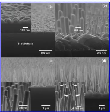
RESULTS AND DISCUSSIONFigure 1 shows the morphological evolution of the ZnO nanostructures obtained with various growth durations. For a
short growth time of 10 min (Figure 1a, sample A), the 1D ZnO nanostructures were just emerging as agglomerated hemispheres with diameter around 100 nm, and the aspect ratio of the ZnO nanostructures was relatively small. It is noted that, similar to those reported previously in density-controlled Ag-nanoisland-catalyzed ZnO-NP arrays,19 the growth of the present ZnO-NPs does not appear to follow the vapor−liquid− solid (VLS) mechanism, as is evident from the absence of catalysis on the growing tips throughout the entire growth process. The inset in Figure 1a is the high-magnification SEM image of sample A. This feature becomes even more apparent in sample B as the growth time is increased to 20 min. As shown in Figure 1b, during this period the ZnO-NPs start to develop from the agglomerated bases along certain crystallo-graphic orientation (the c-axis of wurzite ZnO) with a much reduced pillar diameter andflat tip surface. At this stage, the aspect ratio of the ZnO-NPs has increased to 4−6. As shown in Figure 1c, when the growth time is prolonged to 30 min (sample C), the ZnO-NPs continue to grow preferentially Figure 1. Cross-sectional SEM images of (a) ZnO sample A, (b) sample B, (c) sample C, and (d) sample D. The insets are high-magnification SEM images of sample A, B, C, and D, respectively.
along the c-axis orientation, and the aspect ratio of 15−25 is obtained. It is interesting to note that during this growth stage the growth along the c-axis orientation appears to proceed at the expense of the agglomerated bases and reduction of lateral dimensions. Nevertheless, the tips of the ZnO-NPs remainflat with no sign of residual Au catalyst. Finally, by increasing the growth time to 40 min (sample D), as shown in Figure 1d, preferential growth continues, and the mean aspect ratio of the obtained ZnO-NPs reaches 35−40. More remarkably, at this growth stage, in addition to the continuous increases in the aspect ratio, the morphology of the ZnO-NPs also exhibits some significant changes. It is clearly seen from the insets of Figures 1b−1d that the tip of the ZnO-NPs changes from a flat top appearance (insets of Figure 1b and 1c) to a tapered morphology (as indicated by arrows in the inset of Figure 1d). This pencil-like tip structure substantially reduces the effective radius of the ZnO-NPs and is expected to exhibit significant effects on the field emission properties to be discussed later.
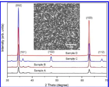
To further delineate the growth mechanism of the current ZnO-NPs and characterize the structural features of all ZnO samples, XRD measurements were carried out, and the results are shown in Figure 2. It shows that all samples are single-phase
wurzite ZnO crystals with two major diffraction peaks corresponding to (002) and (103) crystallographic orientations, respectively. A closer inspection further reveals that, for samples A, B, and C, the intensity of the (002) diffraction peak is dominant over the (103) peak, indicating that during these growth stages the preferred growth orientation is along the c-axis, which is consistent with most of the previous studies. However, for sample D the relative intensity of the (103) diffraction peak becomes more dominant than the (002) diffraction peak, suggesting that with increasing length with prolonged growth time the ZnO-NPs may have either slightly inclined with respect to the [001] normal or started to develop another preferred growth orientation. Judging from Figures 1c−1d and the top-view SEM photograph displayed in Figure 2, the former scenario may be responsible for the observed XRD results.
Furthermore, as mentioned above, since there is no residual catalyst residing on the tips of the present ZnO-NPs, the growth mechanism for the present ZnO-NPs, thus, might be
different from the conventional catalyst-assisted VLS process commonly observed in catalysis-assisted ZnO nanostructure growth. One-dimensional ZnO nanostructures that did not grow exclusively through the classical VLS model had been observed and extensively discussed.19,26,27 It is generally conceived that the presence of metal catalysts is a necessary prerequisite for successful position control during growth, albeit variations may still exist in different process schemes. On the other hand, Zhang et al.29based on thermodynamic arguments proposed that the growth of ZnO 1D-nanostructures may follow the following sequences: (1) the deposited ZnO clusters coalesce and form a layer of ZnOfilm; (2) the film becomes sinuate due to the competing effects between diffusion and surface tension; (3) the sinusoidal-like surface naturally forms crests and hollows; (4) the crests favor the subsequent growth of ZnO nanorods with preferred [001] growth direction. We note that the evolution of ZnO-NPs revealed in Figure 1 appeared to be consistent with the above sequences. Furthermore, the development of pencil-like morphology at the later stage of growth may result from the changing ZnO concentration of the growth ambience due to the depleting Zn source as the growth time elapsed.29,30 In any case, the relatively simple processes practiced in the present study have evidently provided ZnO-NPs with progressively evolving morphological features suitable for investigating the geometrical effects on the field emission properties of ZnO.
However, before performing the comparative field emission measurements, it is also important to examine the intrinsic optoelectronic properties of the obtained ZnO-NPs. For this purpose, the PL measurements have been ubiquitously performed to investigate the intrinsic and defect-associated PL characteristics exhibited in ZnO films and various ZnO nanostructures.31−34In particular, the sub-band-edge emissions from free excitons,35,36surface states,37or impurities38that give rise to characteristic PL peaks have been well-identified, thus providing convenient ways to characterize the crystalline quality of the obtained ZnO samples. Figure 3 shows the PL spectra for samples A−D, exhibiting only emissions from the near band-edge free exciton recombination in the UV range, and the Figure 2.XRD diffraction of ZnO sample A, B, C, and D. The inset is
the top-view SEM image of sample D.
Figure 3.Room temperature PL spectra of ZnO sample A, B, C, and D, respectively. The inset (a) shows the fwhm of the 3.27 eV peak for sample D, and inset (b) shows the purely bluish emission taken from sample D.
visible range emissions associated with surface states and/or crystalline defects are almost completely suppressed. In addition, as shown in the inset (a) of Figure 3, the full-width-at-half-maximum (FWHM) of the UV (3.27 eV) emission peak is only about 84± 0.3 meV, which is much narrower than the previously reported value of 111 meV.39 Since this emission originates primarily from the free exciton recombination, it usually serves as an indicator reflecting the intrinsic crystalline quality of the sample. Inset (b) of Figure 3 further demonstrates that the emission is purely bluish, which is visibly reflecting what one would expect to see based on the results of the PL measurements. All of these evidences strongly indicate that the present ZnO-NPs are indeed with excellent crystalline quality. Interestingly, although the aqueous chemical growth process with lower growth temperatures has been widely advocated and applied to grow ZnO nanostructures, the obtained ZnO nanostructures, however, usually possess a high concentration of structural defects, as indicated by the substantial PL emission intensity in the visible region.40Higher growth temperature, such as 780 °C here, is believed to have the effect of eliminating most of the structural defects, thus blocking the self-compensation processes thermodynamically and removing most of the nonradiative recombination channels.19Moreover, it is noted that the intensity of the free exciton emission at 379 nm (3.27 eV) for sample D (solid circles in Figure 3) was enhanced by nearly an order of magnitude as compared to that of sample A (solid squares in Figure 3), albeit both were deposited under exactly the same conditions. This is attributed to the considerably larger amount of ZnO-NPs grown on the Au-coated Si substrate after prolonged deposition time was practiced. The fact that all the ZnO samples grown on the Au-coated template under exactly the same conditions display essentially the same PL emission characteristics, except for the relative intensities, further indicates the unique feature of the current vapor transport deposition method.41
Figure 4 shows the emission current density as a function of the applied electricalfield (J−E curves) for the as-grown ZnO-NPs. The electricfield was determined by dividing the applied voltage with the apparent cathode−anode separation. Thus, it represents the averaged globalfield instead of local field at the
tips of the ZnO-NPs. The distance between the electrodes was kept at 200μm with the chamber pressure being maintained at 2× 10⁻⁶Torr during measurements. It is evident from Figure 4 that, for the sample A, only diminishingly smallfield emission current was detected up the maximum available appliedfield (5 V/μm) of the current setup. This is presumably due to the extremely unfavorable morphology which may form an insurmountable barrier for emitting electrons. The field emission properties of samples B, C, and D, nonetheless, are improved progressively with increasing aspect ratio of ZnO-NPs. In particular, the pencil-like morphology of sample D evidently exhibits much improved emission characteristics, such as lower turn-on field and higher emission current densities. The relationships between electronic properties and ZnO nanostructures with various morphologies have been reported previously.9−11 According to the classical Fowler−Nordheim (F−N) theory for field emission, the relation between the emission current density and the appliedfield can be expressed by the following F−N equation19
β ϕ ϕ β = ⎛− ⎝ ⎜ ⎞ ⎠ ⎟ J A E B E exp 2 2 3/2 (1) where J is the current density (A/m2); E is the appliedfield (V/
μm); ϕ is the work function (eV); β is the field enhancement factor; and A and B are constants with A = 1.56× 10⁻¹⁰(A·eV/ V2) and B = 6.83× 10³(V/μm·eV3/2), respectively. From eq 1, it is clear that the two primary parameters determining the emission characteristics of a particular structure areϕ and β, which can be obtained experimentally by plotting Sn(J/E2) vs
1/E, the so-called F−N plot. The inset in Figure 4 shows the F−N plot for sample D. It is immediately noted that the F−N plot appears to have two different slopes, suggesting that the field emission behavior of these ZnO-NPs may have deviated from the F−N description slightly.
The two-slope behavior in the F−N plot has been observed in a wide variety of semiconductor nanostructures or even the carbon nanotubes.10,11,42 It was explained on the basis of electron emission from the conduction band (CB) and valence band (VB).11Very recently, Al-Tabbakh et al.43 further took into account the effect of saturation of the conduction band current to reproduce the two-slope F−N plot. Within this scenario, emission from the CB is dominant in the lowerfields. We note here thatϕ = 5.3 eV for ZnO44has been widely cited for emission from the CB. However, if the bottom of the conduction band is considered, the value for electron emission should be taken as 3.8−4.2 eV.21,23,24When the appliedfield is increased further, the electron in the VB (∼3.37 eV below the bottom of the CB) contributes to the emission current together with the electron from the CB. Since the field enhancement factorβ can be calculated from the slope of the F−N plot45
β= −6.83×10³×ϕ3/2/slope (2) which implies that there should be a substantial slope change of 1.64 (ifϕ = 5.3 eV is taken for emission from the CB) to 2.5 times (if the bottom of the conduction band is considered for electron emission) assumingβ remains constant. However, as is evident from the inset of Figure 4, the change of slope in the F−N plots appears to be much milder with only about 10% change. Alternatively, the two-stage emission phenomenon was attributed to the space charge effect, localized state, adsorbate-enhanced tunneling states, and/or variation of local field. Judging from the tapered morphology (Figure 1d) and the Figure 4.Field emission J−E curve from the Au/ZnO-NPs array at a
working distance of 200μm over an effective emitting area of 1 × 1 cm2. The inset is the Fowler−Nordheim plot [ln(J/E2) vs (1/E)] of
optoelectronic properties (Figure 3) of sample D, the observed two-slope behavior is more likely due to the local field variations. A rough estimation on the correspondingβ values for the as-deposited sample D was made from the F−N plot by assumingϕZnO∼ 5.3 eV for ZnO.44The obtainedβ values are 2394 and 2617 for low-field and high-field regimes, respectively. On the other hand, theβ value can also be estimated based on the geometrical parameters21by using
β ≈1+s d r( / ) (3)
where s is the field screening parameter; d is the distance between the emitter tip and the anode; and r is the radius of the emitter tips, respectively. By assuming s≈ 1, and taking d = 200 μm and r ∼ 30 nm, the estimated β value is about 7000. Compared with the values obtained from the F−N plot, it indicates that a substantialfield screening effect with s ≈ 0.3− 0.4 is operating in this case, which is reasonable considering the dense packing of the current ZnO-NPs. Indeed, it has been demonstrated that by properly controlling the density of the ZnO-NPs thefield emission characteristics can be significantly improved.19
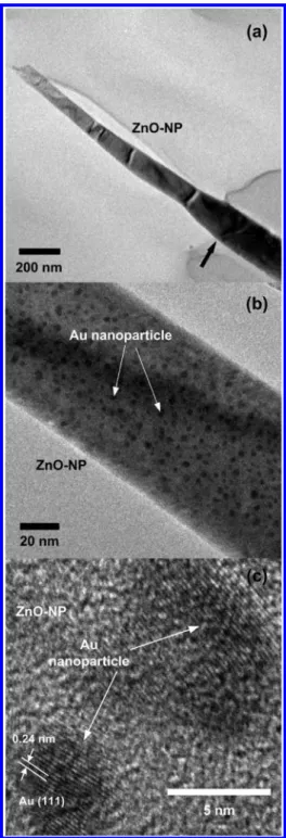
On the other hand, to further harvest the field emission performance from the present ZnO nanostructures and to explore the effect of decorating metal nanoparticles on the field emission properties of the existing nanostructures, Au nano-particles were deposited on samples A−D by a sputter coater to form Au/ZnO heterostructures. A representative low-magni fi-cation TEM image of an individual Au/ZnO-NP (taken from Au-coated sample D) is illustrated in Figure 5a. The tapered feature of the ZnO-NP found in this particular sample is clearly displayed and is indicated by the arrow shown in Figure 5a. Figure 5b shows the enlarged TEM image of the same Au/ ZnO-NP. It is evident from the image that the Au nanoparticles were uniformly dispersed over the entire surface of the ZnO-NP without extended agglomerations. The high-resolution TEM (HRTEM) image displayed in Figure 5c illustrates that the image of the ZnO-NP is slightly out-of-focus, indicating that the Au nanoparticles are“decorating” on the surface of the ZnO-NP instead of “alloying” or “embedding” into the ZnO-NPs. The average diameter of Au nanoparticles obtained from the room-temperature sputtering is about 5−10 nm, and the distance between the two adjacent planes is determined to be 0.24 nm corresponding to the {111} planes of face-center-cubic (fcc) structured Au.
Figure 6 shows the J−E curves for all the Au/ZnO samples (i.e., samples A−D coated with Au). Comparing the data displayed in Figures 4 and 6, it is immediately evident that, except for sample A, the field emission performance is drastically improved by decorating the ZnO-NPs with Au nanoparticles. For instance, for sample D, the turn-on field defined at a current density of 10 μA/cm2is reduced from 3.15 to 2.65 V/μm, while the emission current density at 5 V/μm is increased from 0.44 to 2.11 mA/cm2. The detailed emission properties of the other two Au/ZnO-NP samples are listed together with that of sample D in Table 1. It is noted that the turn-onfield for the present Au/ZnO-NPs is much lower than most of the results obtained from various ZnO nanostructures reported previously,46−50and the emission current density at a similar level of appliedfield (at 5 V/μm limited by the present setup) also outperforms most of the ZnO nanostructures previously reported.49−54Moreover, as can be seen in the inset of Figure 6a, for sample D, not only the above-mentioned two-slope emission feature becomes less pronounced but also theβ
value is increased toβ ≈ 3313 if the same ϕZnO∼ 5.3 eV used in Figure 4 is assumed. Since the morphology of the ZnO-NPs does not change with the decoration of Au nanoparticles, the drastic changes in the field emission properties of sample D must have originated from other mechanisms, such as the charge-transferring-induced electronic band structure changes.20−24 The work function of Au, ϕAu ∼ 4.9 eV,55 is higher (with respect to vacuum level) than ϕZnO ∼ 5.3 eV.
Thus, electron transfer from Au nanoparticles to ZnO-NPs can be expected, which in turn would lead to a downward band-bending on the ZnO side.23The question is by how much and will it account for the observed field emission enhancement Figure 5.(a) Typical low-magnification, (b) high-magnification TEM image, and (c) the HRTEM image of individual Au/ZnO-NP (sample D), respectively.
resulting from Au nanoparticle decoration? If we assume that the change of the slopes in the F−N plots shown in Figure 4 and Figure 6a, instead of being due to change inβ, results from the change in work function due to electron transfer, then from eq 2 we obtainϕAu/ZnO∼ 4.53 eV, about 0.33−0.73 eV below the bottom of the ZnO conduction band.21,23,24 Moreover, since the carrier concentration in the conduction band is related to the Fermi energy by the following expression
π
= * −
n 2(2 m kT h/ )2 3/2exp[(EF EC)/kT] (4) where n, m*, k, h, EF, EC, and T are carrier concentration, effective mass of carriers, Boltzmann constant, Planck constant,
Fermi energy, conduction band energy, and absolute temper-ature, respectively. Taking m* = 0.23m020(with m0being the
mass of free electrons) for ZnO and T = 300 K, a carrier concentration n ≈ 2.90 × 1021 cm−3 is obtained, which is comparable to the value of n≈ 3.77 × 1020cm−3obtained in
Ga-doped ZnO by Xu et al.20We note that the investigations and analyses presented in this study not only give a plausible interpretation to thefield emission characteristics of Au/ZnO-NPs but also point out an efficient way of improving the field emission characteristics in the related nanostructures.
Finally, to check the robustness of the present Au/ZnO-NPs, we have measured the emission current density as a function of time. Figure 6b shows the results of Au on sample D measured with an appliedfield of 4 V/μm. It is evident from the results that the emission current remains quite stable without showing any sign of diminishing over the 1 h period of continuous testing. The variation of the current density is estimated to be about 6 ± 2%, which could arise from factors such as base pressure variation of the vacuum system, temperature of the emitting tips, and so on.
■
CONCLUSIONWe have successfully prepared the well-aligned ZnO-NPs by a traditional vapor transport process on Au-coated Si substrates. The growth mechanism of the obtained ZnO-NPs, however, did not seem to follow the vapor−liquid−solid process commonly observed in metal particle catalyzed growth methods. Moreover, the morphology of the ZnO-NPs was found to evolve with growth time and eventually growing into tapered pillars, presumably due to the decreased Zn source at the later stage of growth. By decorating the ZnO-NPs with Au nanoparticles by sputtering, significant improvements in field emission characteristics were observed. For instance, the Au/ ZnO-NPs exhibited a low turn-onfield of 2.65 V/μm and high current density of 2.11 mA/cm2at an appliedfield of 5 V/μm, which represented a 0.5 V/μm reduction in turn-on field and about 5 times of emission current density at the same applied field as compared to that of the as-prepared ZnO-NPs. The emission current as a function of time test also demonstrated the robustness of the present Au/ZnO-NPs. Detailed analyses on the slope change of the F−N plot indicate the pronounced effects of charge transfer-induced work function reduction in the Au/ZnO-NP heterostructures. The present study has evidently provided an efficient scheme of improving various field-emission-related applications via morphological and electronic modifications of the nanostructures.
■
AUTHOR INFORMATIONCorresponding Author
*Phone: +886-3-5712121, ext. 56116. Fax: +886-3-5725230. E-mail: [email protected] (Y.-M. Chang); [email protected]. edu.tw (J.-Y. Juang).
Notes
The authors declare no competingfinancial interest.
■
ACKNOWLEDGMENTSThis work was partially supported by the National Science Council of Taiwan, under Grant No. NSC 100-2811-M-009-037. Prof. J.-Y. Juang is supported in part by the National Science Council of Taiwan and the MOE-ATP program operated at NCTU. The authors would like to thank Dr. Yu-Hwa Shih, Dr. Jheng-Ming Huang (NCTU), Dr. Shang-Jui Figure 6.(a) Field emission J−E curve from the Au/ZnO-NP array at
working distance of 200μm. The inset is the Fowler−Nordheim plot [ln(J/E2) vs (1/E)] of Au nanoparticles on sample D (circles). (b)
The emission current as a function of time operated at 4 V/μm, showing the robustness of the Au/ZnO-NP nanostructures. Table 1. Key Parameters of Au/ZnO-NP Field Emitters in This Worka
field emitter turn-on-(Vμm−1field)
maximum current density
(mA cm−2) β Au/ZnO sample B 3.30 0.16 2030 Au/ZnO sample C 3.10 0.83 2101 Au/ZnO sample D 2.65 2.11 3313
Chiu (NTHU), and Dr. Yen-Ting Liu (NCTU) for useful discussions.
■
REFERENCES(1) Li, Yu.; Koshizakib, N.; Caia, W. Coord. Chem. Rev. 2011, 255, 357−373.
(2) Weng, W. Y.; Chang, S. J.; Hsu, C. L.; Hsueh, T. J. ACS Appl. Mater. Interfaces 2011, 3, 162−166.
(3) Lupan, O.; Pauporté, T.; Viana, B.; Tiginyanu, I. M.; Ursaki, V. V.; Cortès, R. ACS Appl. Mater. Interfaces 2010, 2, 2083−2090.
(4) Li, Y.; Fang, X.; Koshizaki, N.; Sasaki, T.; Li, L.; Gao, S.; Shimizu, Y.; Bando, Y.; Golberg, D. Adv. Funct. Mater. 2009, 19, 2467−2473.
(5) Guan, J.; Zhang, J.; Yu, T.; Xue, G.; Yu, X.; Tang, Z.; Wei, Y.; Yang, J.; Li, Z.; Zou, Z. RSC Adv. 2012, 2, 7708−7713.
(6) Lee, C. J.; Lee, T. J.; Lyu, S. C.; Zhang, Y.; Ruh, H.; Lee, H. J. Appl. Phys. Lett. 2002, 81, 3648−3650.
(7) Xu, C. X.; Sun, X. W. Appl. Phys. Lett. 2003, 83, 3806−3808. (8) Li, Y. B.; Bando, Y.; Golberg, D. Appl. Phys. Lett. 2004, 84, 3603− 3605.
(9) Zhao, Q.; Zhang, H. Z.; Zhu, Y. W.; Feng, S. Q.; Sun, X. C.; Xu, J.; Yu, D. P. Appl. Phys. Lett. 2005, 86, 203115−1−3.
(10) Xu, C. X.; Sun, X. W.; Fang, S. N.; Yang, X. H.; Yu, M. B.; Zhu, G. P.; Cui, Y. P. Appl. Phys. Lett. 2006, 88, 161921−1−3.
(11) Premkumar, T.; Zhou, Y. S.; Lu, Y. F.; Baskar, K. ACS Appl. Mater. Interfaces 2010, 2, 2863−2869.
(12) Bekermann, D.; Gasparotto, A.; Barreca, D.; Bovo, L.; Devi, A.; Fischer, R. A.; Lebedev, O. I.; Maccato, C.; Tondello, E.; Tendeloo, G. V. Cryst. Growth Des. 2010, 10, 2011−2018.
(13) Barreca, D.; Bekermann, D.; Devi, A.; Fischer, R. A.; Gasparotto, A.; Maccato, C.; Tondello, E.; Rossi, M.; Orlanducci, S.; Terranova, M. L. Chem. Phys. Lett. 2010, 500, 287−290.
(14) Barreca, D.; Bekermann, D.; Comini, E.; Devi, A.; Fischer, R. A.; Gasparotto, A.; Maccato, C.; Sada, C.; Sberveglieric, G.; Tondello, E. CrystEngComm 2010, 12, 3419−3421.
(15) Simon, Q.; Barreca, D.; Gasparotto, A.; Maccato, C.; Tondello, E.; Sada, C.; Comini, E.; Devi, A.; Fischer, R. A. Nanotechnology 2012, 23, 025502−1−7.
(16) Bekermann, D.; Gasparotto, A.; Barreca, D.; Devi, A.; Fischer, R. A.; Kete, M.; Štangar, U. L.; Lebedev, O. I.; Maccato, C.; Tondello, E.; Tendeloo, G. V. ChemPhysChem 2010, 11, 2337−2340.
(17) Simon, Q.; Barreca, D.; Bekermann, D.; Gasparotto, A.; Maccato, C.; Comini, E.; Gombac, V.; Fornasiero, P.; Lebedev, O. I.; Turner, S.; Devi, A.; Fischer, R. A.; Tendeloo, G. V. Int. J. Hydrogen Energy 2011, 36, 15527−15537.
(18) Simon, Q.; Barreca, D.; Gasparotto, A.; Maccato, C.; Montini, T.; Gombac, V.; Fornasiero, P.; Lebedev, O. I.; Turner, S.; Tendeloo, G. V. J. Mater. Chem. 2012, 22, 11739−11747.
(19) Chang, Y.-M.; Huang, J. M.; Lin, C.-M.; Lee, H.-Y.; Chen, S.-Y.; Juang, J.-Y. J. Phys. Chem. C 2012, 116, 8332−8337.
(20) Xu, C. X.; Sun, X. W.; Chen, B. J. Appl. Phys. Lett. 2004, 84, 1540−1542.
(21) Ye, C.; Bando, Y.; Fang, X.; Shen, G.; Golberg, D. J. Phys. Chem. C 2007, 111, 12673−12676.
(22) Daniel, M. C.; Astruc, D. Chem. Rev. 2004, 104, 293−346. (23) Wang, X.; Kong, X.; Yu, Y.; Zhang, H. J. Phys. Chem. C 2007, 111, 3836−3841.
(24) Im, J.; Singh, J.; Soares, J. W.; Steeves, D. M.; Whitten, J. E. J. Phys. Chem. C 2011, 115, 10518−10523.
(25) Zhao, D.; Andreazza, C.; Andreazza, P.; Ma, J.; Liu, Y.; Shen, D. Chem. Phys. Lett. 2005, 408, 335−338.
(26) Fan, H. J.; Lee, W.; Hauschild, R.; Alexe, M.; Rhun, G. L.; Scholz, R.; Dadgar, A.; Nielsch, K.; Kalt, H.; Krost, A.; Zacharias, M.; Gösele, U. Small 2006, 2, 561−568.
(27) Zhang, Z.; Wang, S. J.; Yu, T.; Wu, T. J. Phys. Chem. C 2007, 111, 17500−17505.
(28) Chang, Y.-M.; Liu, M.-C.; Kao, P.-H.; Lin, C.-M.; Lee, H.-Y.; Juang, J.-Y. ACS Appl. Mater. Interfaces 2012, 4, 1411−1416.
(29) Zhang, Z.; Yuan, H.; Zhou, J.; Liu, D.; Luo, S.; Miao, Y.; Gao, Y.; Wang, J.; Liu, L.; Song, L.; Xiang, Y.; Zhao, X.; Zhou, W.; Xie, S. J. Phys. Chem. B 2006, 110, 8566−8569.
(30) She, J.; Xiao, Z.; Yang, Y.; Deng, S.; Chen, J.; Yang, G.; Xu, N. ACS Nano 2008, 2, 2015−2022.
(31) Fonoberov, V. A.; Balandin, A. A. Phys. Rev. B 2004, 70, 195410−1−5.
(32) Kar, A.; Kundu, S.; Patra, A. RSC Adv. 2012, 2, 4879−4885. (33) Chiang, T.-Y.; Dai, C.-L.; Lian, D.-M. J. Alloys Compd. 2011, 509, 5623−5626.
(34) Xue, X.-Y.; Chen, Z.-H.; Xing, L.-L.; Ma, C.-H.; Chen, Y.-J.; Wang, T.-H. J. Phys. Chem. C 2010, 114, 18607−18611.
(35) Chang, Y.-M.; Shieh, J.; Chu, P.-Y.; Lee, H.-Y.; Lin, C.-M.; Juang, J.-Y. ACS Appl. Mater. Interfaces 2011, 3, 4415−4419.
(36) Chang, Y.-M.; Kao, P.-H.; Liu, M.-C.; Lin, C.-M.; Lee, H.-Y.; Juang, J.-Y. RSC Adv. 2012, 2, 11089−11094.
(37) Chang, Y.-M.; Jian, S.-R.; Lee, H.-Y.; Lin, C.-M.; Juang, J.-Y. Nanotechnology 2010, 21, 385705−1−7.
(38) Garces, N. Y.; Wang, L.; Bai, L.; Giles, N. C.; Halliburton, L. E.; Cantwell, G. Appl. Phys. Lett. 2002, 81, 622−624.
(39) Kong, Y. C.; Yu, D. P.; Zhang, B.; Fang, W.; Feng, S. Q. Appl. Phys. Lett. 2001, 78, 407−409.
(40) Panigrahi, S.; Basak, D. Nanoscale 2011, 3, 2336−2341. (41) Jo, S. H.; Lao, J. Y.; Ren, Z. F.; Farrer, R. A.; Baldacchini, T.; Fourkas, J. T. Appl. Phys. Lett. 2003, 83, 4821−4823.
(42) Ramgir, N. S.; Late, D. J.; Bhise, A. B.; Mulla, I. S.; More, M. A.; Joag, D. S.; Pillai, V. K. Nanotechnology 2006, 17, 2730−2735.
(43) Al-Tabbakh, A. A.; More, M. A.; Joag, D. S.; Mulla, I. S.; Pillai, V. K. ACS Nano 2010, 4, 5585−5590.
(44) Li, C.; Fang, G.; Liu, N.; Li, J.; Liao, L.; Su, F.; Li, G.; Wu, X.; Zhao, X. J. Phys. Chem. C 2007, 111, 12566−12571.
(45) Kale, V. S.; Prabhakar, R. R.; Pramana, S. S.; Rao, M.; Sow, C.-H.; Jinesh, K. B.; Mhaisalkar, S. G. Phys. Chem. Chem. Phys. 2012, 14, 4614−4619.
(46) Pradhan, D.; Kumar, M.; Ando, Y.; Leung, K. T. ACS Appl. Mater. Interfaces 2009, 4, 789−796.
(47) Shen, X.-P.; Yuan, A.-H.; Hu, Y.-M.; Jiang, Y.; Xu, Z.; Hu, Z. Nanotechnology 2005, 16, 2039−2043.
(48) Zhang, Y.; Lee, C.-T. J. Phys. Chem. C 2009, 113, 5920−5923. (49) Liu, J.; Huang, X.; Li, Y.; Ji, X.; Li, Z.; He, X.; Sun, F. J. Phys. Chem. C 2007, 111, 4990−4997.
(50) Ahmad, M.; Sun, H.; Zhu, J. ACS Appl. Mater. Interfaces 2011, 3, 1299−1305.
(51) Cao, B.; Teng, X.; Heo, S. H.; Li, Y.; Cho, S. O.; Li, G.; Cai, W. J. Phys. Chem. C 2007, 111, 2470−2476.
(52) Marathe, S. K.; Koinkar, P. M.; Ashtaputre, S. S.; More, M. A.; Gosavi, S. W.; Joag, D. S.; Kulkarni, S. K. Nanotechnology 2006, 17, 1932−1936.
(53) Zhang, Z.; Meng, G.; Xu, Q.; Hu, Y.; Wu, Q.; Hu, Z. J. Phys. Chem. C 2010, 114, 189−193.
(54) Wu, L.; Li, Q.; Zhang, X.; Zhai, T.; Bando, Y.; Golberg, D. J. Phys. Chem. C 2011, 115, 24564−24568.
(55) Wang, S. Fundamentals of Semiconductor Theory and Device Physics; Prentice-Hall Inc.: NJ, 1989; p 131.