Impacts of a polycrystalline-silicon buffer layer on the performance and reliability of
strained n -channel metal-oxide-semiconductor field-effect transistors with SiN capping
Ching-Sen Lu, Horng-Chih Lin, Jian-Ming Huang, and Yao-Jen Lee
Citation: Applied Physics Letters 90, 122110 (2007); doi: 10.1063/1.2715122 View online: http://dx.doi.org/10.1063/1.2715122
View Table of Contents: http://scitation.aip.org/content/aip/journal/apl/90/12?ver=pdfcov
Published by the AIP Publishing
Articles you may be interested in
Impact of halo implant on the hot carrier reliability of germanium p -channel metal-oxide-semiconductor field-effect transitors
J. Vac. Sci. Technol. B 29, 01A804 (2011); 10.1116/1.3520647
Behaviors of gate induced drain leakage stress in lightly doped drain n -channel metal-oxide-semiconductor field-effect transistors
Appl. Phys. Lett. 95, 152107 (2009); 10.1063/1.3250435
Performance enhancement of n -channel inversion type In x Ga 1 x As metal-oxide-semiconductor field effect transistor using ex situ deposited thin amorphous silicon layer
Appl. Phys. Lett. 93, 122109 (2008); 10.1063/1.2991340
Strained Si n -channel metal-oxide-semiconductor field-effect transistors formed on very thin SiGe relaxed layer fabricated by ion implantation technique
Appl. Phys. Lett. 90, 202101 (2007); 10.1063/1.2739324
On the beneficial impact of tensile-strained silicon substrates on the low-frequency noise of n -channel metal-oxide-semiconductor transistors
Appl. Phys. Lett. 86, 223509 (2005); 10.1063/1.1942631
This article is copyrighted as indicated in the article. Reuse of AIP content is subject to the terms at: http://scitation.aip.org/termsconditions. Downloaded to IP: 140.113.38.11 On: Thu, 01 May 2014 00:37:25
Impacts of a polycrystalline-silicon buffer layer on the performance
and reliability of strained n-channel metal-oxide-semiconductor
field-effect transistors with SiN capping
Ching-Sen Lu
Institute of Electronics, National Chiao Tung University, Hsinchu 300, Taiwan
Horng-Chih Lina兲
Institute of Electronics, National Chiao Tung University, Hsinchu 300, Taiwan and National Nano Device Laboratories, Hsinchu 300, Taiwan
Jian-Ming Huang
Institute of Electronics, National Chiao Tung University, Hsinchu 300, Taiwan
Yao-Jen Lee
National Nano Device Laboratories, Hsinchu 300, Taiwan
共Received 7 November 2006; accepted 15 February 2007; published online 20 March 2007兲 Characteristics of n-channel metal-oxide-semiconductor field-effect transistors with SiN capping were investigated in this work. Although the SiN capping could dramatically enhance the carrier mobility and thus the device drive current, the resistance to hot-carrier degradation is compromised as well, owing to the large amount of hydrogen contained in the SiN layer which may diffuse into the channel region during the process. To eliminate this shortcoming, the insertion of an ultrathin 共10 nm兲 polycrystalline-silicon buffer layer between the gate and the SiN capping was proposed and demonstrated to restore the hot-carrier reliability of the devices without compromising the current enhancement due to the SiN capping. © 2007 American Institute of Physics.
关DOI:10.1063/1.2715122兴
Channel-strain engineering has emerged as one of the most effective remedies to boost the drive current in the scaled devices.1–5 This could be done by either applying a high biaxial tensile strain to the channel region with a SiGe virtual substrate,1 or uniaxially straining the channel with strain boosters, such as stress liner,2 embedded SiC in the source/drain 共S/D兲 region,3 and shallow trench isolation.4 Among these approaches, a SiN capping layer over the gate of n-channel metal-oxide-semiconductor field-effect-transistors 共NMOSFETs兲 serving as the contact etch-stop layer has demonstrated its potential for large performance gains.5Such scheme is attractive and practical because it can be easily implemented using integrated circuit processing. Nevertheless, attentions should now be focused on the asso-ciated reliability issues for practical applications. Currently, device degradation caused by hot carriers represents one of the most critical reliability issues in strain-channel NMOSFETs.6,7Although the physical mechanisms and char-acteristics of hot electron degradation have been extensively examined,8,9 there seems to be very few works that investi-gate the impact of SiN capping. Furthermore, the deposition of a buffer layer prior to the SiN capping on the hot-carrier reliability of the strained devices has not been reported in literature. In this work, we clearly demonstrated that the in-sertion of an undoped ultrathin polycrystalline silicon 共poly-Si兲 is useful in relieving the aggravated hot-carrier degrada-tion caused by the SiN capping layer.
NMOSFETs characterized in this study were with 3 nm thermal oxide grown in a vertical furnace in O2 at 800 ° C,
and 150-nm-thick n+poly-Si layer as the gate electrode.
Af-ter the gate formation, most samples were capped with a SiN layer of 300 nm, deposited by a low-pressure chemical vapor deposition 共LPCVD兲 system 共denoted as the SiN-capped split兲; the SiN deposition step was deliberately skipped for some wafers to serve as the controls共denoted as the control split兲. For some SiN-capped samples, a thin undoped poly-Si buffer layer of 10 nm was capped prior to the SiN deposition 共denoted as the BL-POLY split兲. The SiN deposition was performed at 780 ° C with SiH2Cl2 and NH3 as the reaction
precursors. For some of the SiN-capped wafers, the SiN layer was deliberately removed after deposition in order to evaluate the impact of SiN deposition process itself on the device performance共denoted as SiN-removal split兲. The top-mast passivation layer of all wafers is a 300-nm-thick tetra-ethoxysilane layer, followed by contact holes and metalliza-tion processes. To clarify the effect associated with the thermal budget of SiN deposition, the control split received a placebo annealing in N2ambient at the same temperature and
duration as those of SiN deposition process. Finally, the pro-cessing steps were completed with a forming gas annealing at 400 ° C. Electrical characterizations were performed using an HP 4156 system.
The stress induced by LPCVD-SiN layer with and with-out 10-nm-thick poly-Si buffer layer was first examined by probing the blanket films deposited on bare Si wafers. We confirmed that the stresses are tensile in nature with a mag-nitude of around 300 MPa for all samples, irrespective of poly-Si presence. Figure1shows the percentage increase of transconductance with respect to the control samples for SiN-capped, BL-POLY, and SiN-removal samples, as a func-tion of channel length. We can see that the transconductance enhancement reaches about 33% at a channel length of 0.4m for SiN-capped and BL-POLY samples. When SiN
a兲Electronic mail: [email protected]
APPLIED PHYSICS LETTERS 90, 122110共2007兲
0003-6951/2007/90共12兲/122110/3/$23.00 90, 122110-1 © 2007 American Institute of Physics
This article is copyrighted as indicated in the article. Reuse of AIP content is subject to the terms at: http://scitation.aip.org/termsconditions. Downloaded to IP: 140.113.38.11 On: Thu, 01 May 2014 00:37:25
capping is removed, the enhancement diminishes. These ob-servations demonstrate the following. 共1兲 The transconduc-tance enhancement is indeed due to the uniaxial tensile strain by SiN capping which increases with decreasing channel length.共2兲 The insertion of 10-nm-thick poly-Si between the gate and the SiN capping does not compromise such perfor-mance enhancement. These electrical results are consistent with the film stress measurements. The inset in Fig.1shows the capacitance-voltage共C-V兲 characteristics for all samples. Basically all C-V curves are identical, indicating that the above observations are not caused by the oxide thickness difference among all splits.
Next we shift our attention to the hot-carrier character-ization and study the effectiveness of using poly-Si buffer layer in improving the hot-carrier resistance. Figure2shows the substrate current共Isub兲 versus gate voltage for all splits of devices. It can be seen that the substrate currents of the SiN-capped samples and the BL-POLY samples depict similar trends, and both are larger than that of the control counter-parts. When SiN is removed, the substrate current becomes comparable to that of the control devices. These results indi-cate that the channel strain plays an important role in affect-ing the generation of channel hot electrons and the associated impact ionization process. In addition, a thin poly-Si buffer layer of 10 nm does not seem to release the stress induced by the SiN capping because of the similar maximum substrate current 共Isub,max兲, and is consistent with the inference
de-duced from Fig.1. Origins for the increase in substrate cur-rent for the strained samples are ascribed to the band gap
narrowing effect induced by the channel strain as well as the increased mobility, both tend to enhance the impact ioniza-tion rate.10,11
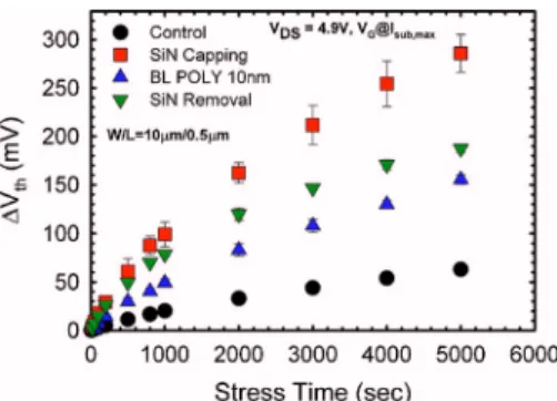
Hot-carrier stressing for all splits of samples were per-formed at VDS= 4.9 V and VGS at the maximum substrate
current. Channel length and width of the test devices are 0.5 and 10m, respectively. Figure 3 shows threshold voltage shift as a function of stress time. We can see that the SiN-capped samples depict the worst degradation in terms of the largest threshold voltage shift, while samples with a thin poly-Si buffer layer apparently show improvement in hot-carrier degradation. It is speculated that the increased hot-carrier mobility in strained channel devices and abundant hydrogen contained in SiN capping are the two primary culprits for the aggravated hot-carrier degradation.11,12The increased carrier mobility may increase the device substrate current, as evi-denced in Fig.2, leading to higher degradation. On the other hand, the deposited SiN contains a large amount of hydrogen species which may diffuse into the gate oxide and channel region. It is well known that the breaking of Si–H bonds is one of the major origins responsible for the hot-carrier damage,8,9 the voluminous hydrogen species definitely ag-gravate the reliability. This is evidenced in the figure as the SiN-removal devices depict much severe degradation than the control and BL-POLY ones, even though the channel strain has been eliminated by the SiN removal. The phenom-enon clearly indicates that the SiN deposition process itself may result in the enhanced damage effect in the short-channel devices.
Figure 4共a兲shows several possible pathways for hydro-gen diffusion in SiN-capped samples, namely, through the gate electrode 共path A1兲 or oxide spacer 共path A2兲 into the gate oxide and channel region, or through the S/D contacts into the Si substrate and diffuse laterally into the channel region 共path A3兲. The results shown in Fig. 3 for SiN-removal samples imply that such diffusion processes occur during the SiN deposition. It has been previously pointed out that the grain boundaries in poly-Si films act as efficient traps for hydrogen,13,14 explaining the observation that the diffusivity of hydrogen is significantly reduced as compared with that in oxide13and in monocrystalline Si.13,14This indi-cates the A1 path is not preferred for hydrogen diffusion. Similarly, samples with the deposition of a poly-Si buffer layer prior to the SiN capping can effectively suppress the diffusion of hydrogen species into these regions from the pathways mentioned above, as shown in Fig.4共b兲. As a re-sult, less broken Si–H bonds and thus less generated inter-FIG. 1. 共Color online兲 Percentage increase of transconductance vs channel
length for different splits of samples with respect to the control ones. Each datum point represents the mean measurement value from six devices. Inset: capacitance-voltage共C-V兲 characteristics for all splits. Basically all C-V curves are identical, indicating the transconductance increase is not caused by the oxide thickness difference among all splits.
FIG. 2. 共Color online兲 Substrate current vs gate voltage for different splits with channel width/length of 10/ 0.5m.
FIG. 3. 共Color online兲 Vthshift as a function of stress time. Devices with channel width/length of 10/ 0.5m were stressed at VDS= 4.9 V, and VGof
maximum substrate current. Each datum point represents the mean measure-ment value from three devices.
122110-2 Lu et al. Appl. Phys. Lett. 90, 122110共2007兲
This article is copyrighted as indicated in the article. Reuse of AIP content is subject to the terms at: http://scitation.aip.org/termsconditions. Downloaded to IP: 140.113.38.11 On: Thu, 01 May 2014 00:37:25
face state compared with the SiN-capped samples without buffer are observed. As a consequence, BL-POLY samples show better reliability characteristics than SiN-capped ones. In summary, this work shows convincing evidence that the diffusion of hydrogen during the deposition of SiN layer is mainly responsible for the worsened hot-carrier damage in strained-channel NMOSFETs. Since the grain boundaries in poly-Si can effectively suppress the hydrogen diffusion,13,14 the use of an ultrathin undoped poly-Si buffer layer prior to the SiN capping can effectively improve hot-carrier
reliabil-ity of the devices without compromising device performance enhancement.
This work was supported in part by the National Science Council under Contract No. NSC95-2221-E-009-297.
1J. L. Hoyt, H. M. Nayfeh, S. Eguchi, I. Aberg, G. Xia, T. Drake, E. A.
Fitzgerald, and D. A. Antoniadis, Tech. Dig. - Int. Electron Devices Meet.
2002, 23.
2C. Y. Lu, H. C. Lin, and T. Y. Huang, Electrochem. Solid-State Lett. 9,
138共2006兲.
3Kah-Wee Ang, King-Jien Chui, Hock-Chun Chin, Yong-Lim Foo, Anyan
Du, Wei Deng, Ming-Fu Li, Ganesh Samudra, N. Balasubramanian, and Yee-Chia Yeo, Tech. Dig. Symp. on VLSI Technol., 90共2006兲.
4K. Ota, T. Yokoyama, H. Kawasaki, M. Moriya, T. Kanai, S. Takahashi, T.
Sanuki, E. Hasumi, T. Komoguchi, Y. Sogo, Y. Takasu, K. Eda, A. Oishi, K. Kasai, K. Ohno, M. Iwai, M. Saito, F. Matsuoka, N. Nagashima, T. Noguchi, and Y. Okamoto, Tech. Dig. Symp. on VLSI Technol., 138 共2005兲.
5S. E. Thompson, G. Sun, K. Wu, J. Lim, and T. Nishida, Tech. Dig. - Int.
Electron Devices Meet. 2004, 221.
6D. Onsongo, D. Q. Kelly, S. Dey, R. L. Wise, C. R. Cleavelin, and S. K.
Banerjee, IEEE Trans. Electron Devices 38, 2193共2004兲.
7S. Dey, M. Agostinelli, C. Prasad, X. Wang, and L. Shifren, Proceedings of the International Reliability Physics Symposium, 2006, pp. 461–464. 8R. B. Fair and R. C. Sun, IEEE Trans. Electron Devices 28, 83共1981兲. 9M. Shimaya, Proceedings of the International Reliability Physics
Sympo-sium, 1995, pp. 292–296.
10T. Hoshii, S. Sugahara, and S. Takagi, International Conference on Solid State Devices and Materials, 2006, pp. 164–165.
11M. F. Lu, S. Chiang, A. Liu, S. H. Lu, M. S. Yeh, J. R. Hwang, T. H. Tang,
W. T. Shiau, M. C. Chen, and T. Wang, Proceedings of the International
Reliability Physics Symposium, 2004, pp. 18–22.
12C. Y. Lu, C. S. Lu, Y. L. Hsieh, Y. J. Lee, H. C. Lin, and T. Y. Huang, International Conference on Solid State Devices and Materials, 2006, pp.
528–529.
13W. B. Jackson, N. M. Johnson, C. C. Tsai, I.-W. Wu, A. Chiang, and D.
Smith, Appl. Phys. Lett. 61, 1670共1992兲.
14N. H. Nickel, W. B. Jackson, and J. Walker, Phys. Rev. B 53, 7750
共1996兲. FIG. 4.共Color online兲 共a兲 In SiN-capped devices, a large amount of
hydro-gen species from the SiN layer diffuse to the gate oxide layer and the channel region through three possible pathways denoted as A1, A2, and A3. 共b兲 In BL-POLY devices, the diffusion of hydrogen species from SiN is suppressed by the poly-Si buffer layer.
122110-3 Lu et al. Appl. Phys. Lett. 90, 122110共2007兲
This article is copyrighted as indicated in the article. Reuse of AIP content is subject to the terms at: http://scitation.aip.org/termsconditions. Downloaded to IP: 140.113.38.11 On: Thu, 01 May 2014 00:37:25