QUALITY AND RELIABILITY ENGINEERING INTERNATIONAL Qual. Reliab. Engng. Int. 2000; 16: 99–116
IMPLEMENTATION OF PETRI NETS USING A
FIELD-PROGRAMMABLE GATE ARRAY
S. K. YANG1∗AND T. S. LIU2
1Department of Mechanical Engineering, National Chin Yi Institute of Technology, Taichung 411, Taiwan, Republic of China 2Department of Mechanical Engineering, National Chiao Tung University, Hsinchu 300, Taiwan, Republic of China
SUMMARY
Although Petri nets have various capabilities, the Petri net approach is done on paper. A field-programmable gate array (FPGA) is implemented in this study so as to realize basic Petri net symbols, logic structures in Petri nets, and specific functions for Petri nets by logic circuits. As an example, a Petri net for an early failure detection and isolation arrangement (EFDIA) is implemented as an application-specific integrated circuit (ASIC) on a Xilinx Demonstration Board. This ASIC is verified by three simulations dealing with three different failure scenarios of a system, and the ASIC functions identically to the EFDIA Petri net. Accordingly, not only the EFDIA Petri net but also any specific function Petri nets can be implemented by FPGA circuits. Copyright2000 John Wiley & Sons, Ltd.
KEY WORDS: Petri net implementation; FPGA; preventive maintenance; logic circuit; ASIC
1. INTRODUCTION
Sequential machines are composed of sequential logic circuits. A sequential machine operates according to a set of sequential conditions. These conditions constitute states of the machine. Therefore sequential machines are called state machines [1]. A state machine is a synchronous machine if transitions between states are driven by clock pulses. On the other hand, asynchronous machines are driven by changes of inputs, i.e. transitions between states may occur at any time. There are two categories of state machines, namely Moore machines and Mealy machines. The output of a Moore machine is only related to states of the machine, whereas a Mealy machine is related to states and inputs of the machine [2]. State machines have been widely used in design work in many fields owing to systematic hardware design methods and tangible implementation models. They support not only synchronous but also asynchronous implementations, which are efficient and easy to design [3].
Petri nets [4] belong to the state machine family and offer good modelling capability in parallelism and synchronization. Accordingly, they are suitable to perform modelling, analysis, verification, reduction,
∗Correspondence to: S. K. Yang, Department of Mechanical
Engineering, National Chin Yi Institute of Technology, Taichung 411, Taiwan, Republic of China. Email: [email protected].
synthesis [3], etc. A system can be modelled into Petri nets to express not only static behaviours such as logical relations between components of the system, but also dynamic behaviours such as operating sequence or failure occurrence of the system. Although Petri nets have various capabilities, the Petri net approach is done on paper. However, because Petri nets are state machines, it is feasible to realize Petri nets to perform those capabilities. Petri nets can be represented by software or hardware approaches. Software implementation for Petri nets using computer language, e.g. Prolog and CSPL, usually takes a long time [5]. Hardware implementation is to realize state machines that are converted from Petri nets to logic circuits. Hardware implementation can be done by choosing one adequate device from the logic device families [6] according to the application, the complexity and the properties of the Petri net.
The advances in semiconductor manufacturing technology enable the production of higher-density integrated circuits (ICs) such as VLSI (very-large-scale IC) or ULSI (ultra-large-(very-large-scale IC). Nowadays, ICs are becoming smaller and more powerful but faster and cheaper. As a result, application-specific integrated circuits (ASICs) are widely used. In practice, Petri nets can be implemented as ASICs so as to perform specific functions without user intervention. Early failure detection and isolation
Received 14 April 1999
100 S. K. YANG AND T. S. LIU
depicted in Reference [7], for example, can be implemented as an ASIC. Furthermore, the ASIC with early failure detection and isolation function can be incorporated into a system to assist in the decision making on preventive maintenance (PM) for the system. Generally speaking, there are four different approaches to ASIC design [8].
1. Full custom. All design works, from logic design to layout and wire routing, are done by a designer according to requests from the customer. This method has the widest design flexibility and the highest efficiency of the wafer. On the other hand, it needs the longest design time, experienced personnel and the highest non-recurring engineering (NRE) cost. Moreover, the product function is specific and with low interchangeability.
2. Standard cell. Designers perform design works by using circuits in the existing cell library. If the needed circuit is not available, it will be designed or purchased and then added to the cell library. In contrast to full custom design, this method saves design time and increases design flexibility. 3. Gate array. It is made of the semi-manufactured
wafer, which has logic gates in array form, to execute design works merely by designing the metal layer so as to connect the gates to the desired IC. This method reduces the use of masks for many layers of the wafer such that the NRE cost is lowered. However, the wafer area is increased owing to the fixed arrangement of the array.
4. Programmable logic device (PLD). PLDs are manufactured from existing structures such as RAM, ROM or PLA [6], which enables designers to write (for EEPROM-based components) or download (for SRAM-based components) the designed circuits to the PLD so as to perform on-line verification. Consequently, it is not necessary to manufacture a prototype IC by wafer factory and package factory to verify its function. Hence this method saves the most design time and NRE cost. FPGAs and CPLDs are main tools for this type of design.
2. FIELD-PROGRAMMABLE GATE ARRAY
Mainly because of its programmable capability, the field-programmable gate array (FPGA) is becoming popular not only in industry but also in academia. The main features of FPGAs [6] are stated below.
1. Field-programmable. FPGAs can be programmed by end-users. This feature saves the time spent in factories including manufacturing and waiting.
2. Reprogrammable. This feature makes FPGAs suitable for teaching and research.
3. Rapid prototyping. The downloaded FGPA itself is a prototype of the newly developing product. 4. No IC test and NRE cost. FPGAs avoid the NRE
cost and promote the efficiency of debugging by vendor-supported simulation software or simulator.
5. Fast time of market. Newly developed products are put on the market in a short time.
6. In-circuit design verification.
Based on the above features, FPGAs are suitable for hardware implementation of Petri nets. This study employs a Xilinx FPGA [9] as the design tool to implement Petri nets.
3. CIRCUITS CONVERTED FROM PETRI NETS By using Xilinx Foundation [9], each of the Petri net-converted circuits can be generated as a macro symbol for the schematic toolbox. Detailed circuits of corresponding macro symbols can be observed by hierarchical push-and-pop functions.
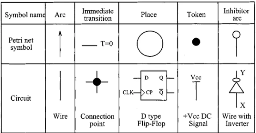
3.1. Petri net symbols
The following five items are basic symbols for Petri nets [10]. Corresponding circuits are shown in Figure1.
1. Place, drawn as a circle, denotes event. A place can be converted to a D-type flip-flop, which represents the associated event occurrence by output high Q. Q is high if D is high at the rising edge of the clock pulses.
2. Token, drawn as a dot, contained in places, denoting the data. In logic circuits, token can be represented as a logic high signal.
3. Arc, drawn as an arrow, between places and transitions. Arcs are connection wires between components.
4. Immediate transition, drawn as a thin bar, denoting event transfer with no delay time. Therefore a connection point represents it. 5. Inhibitor arc, drawn as a line with a circle end,
between places and transitions. An inhibitor arc can be converted to a connection wire with an inverter. It inverts the relation between input (X) and output (Y).
IMPLEMENTATION OF PETRI NETS 101
Figure 1. Corresponding circuits for basic Petri net symbols
Figure 2(a). Structures of basic logic relations for Petri nets and corresponding circuits
3.2. Structures of basic logic relations
Basic logic structures of Petri nets and associated logic circuits are presented below and illustrated in Figures 2(a)–2(e), where X, Y and CLK represent input place, output place and clock respectively. All D-type flip-flops are positive edge triggered.
1. TRANSFER. The token (logic high signal in the circuit) in X transfers to Y through transition T without delay time.
2. AND. Both X1 and X2 are signal high then Y is high.
3. OR. Either X1 or X2 is high then Y is high. 4. TRANSFER AND. In this configuration, X feeds
high signal to both Y1 and Y2. It describes the situation that X holds, then Y1 and Y2 hold at the same time.
5. TRANSFER OR. X flip-flop triggers either Y1 or Y2 depending on the earlier occurred event between X1 and X2. It is a conditional
102 S. K. YANG AND T. S. LIU
Figure 2(b). Structures of basic logic relations for Petri nets and corresponding circuits
IMPLEMENTATION OF PETRI NETS 103
Figure 2(d). Structures of basic logic relations for Petri nets and corresponding circuits
configuration that was described in Reference [7]. 6. IDENTITY. It is a self-content circuit, which
supplies a token at any time for Petri nets. 7. INVERT (COMPLEMENT). The relation
be-tween X and Y is always inverted.
8. INHIBITION. The condition for high Y is low X1 but high X2. It inhibits Y to be high whenever X1 event occurs.
9. IMPLICATION. Y is triggered either by low X1 or by high X2.
10. NAND. Y is high if both X1 and X2 are low. The transition T1 in Petri nets is involved in the NAND gate such that T1 cannot be seen in the logic circuit.
11. NOR. Y is triggered when both X1 and X2 are low.
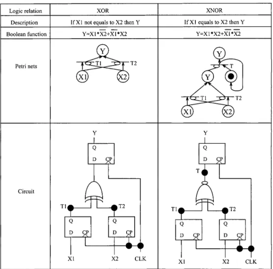
12. XOR. Y is high if X1 is not equal to X2. This configuration is used to verify whether X1 and X2 are not the same.
13. XNOR. XNOR is the complement of XOR, which is used to verify whether X1 and X2 are the same.
Generally, relations between places in a Petri net are constructed by the above logic structures. Each circuit for the structures can be generated into the toolbox as a macro symbol for ease of Petri net circuit design.
3.3. Specific function arrangements
1. Reset. This function is used to release the token that is held in a place by generating a token to fire the output transition of the place. Since a token is implemented by a logic high signal, the reset function can be implemented as a push button with a Vcc input.
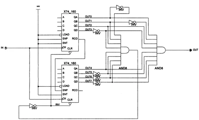
2. Counter. It is used to count and record event occurrence times. There are various types of counters in Xilinx XACT libraries [11]. In a Petri net dealing with system failures, the counter should count up to a sufficient number and be able to be cleared asynchronously. Therefore a 4-bit cascade binary counter with clock enable and asynchronous clear (CB4CE) is adopted in
104 S. K. YANG AND T. S. LIU
Figure 2(e). Structures of basic logic relations for Petri nets and corresponding circuits
IMPLEMENTATION OF PETRI NETS 105
Figure 5. Circuit of FREQDIV15
this study. The CB4CE is shown in Figure3and pin functions are described as follows.
(1) CE is the clock enable input, which is used to enable the counter itself.
(2) C stands for the clock.
(3) Q0, Q1, Q2 and Q3 constitute four data output bits. They increment when the CE is high during the low-to-high clock transition. (4) CEO is the counter enable output, which is
used to enable the next stage counter. (5) TC denotes terminal count. It is high when
all Qs are high.
(6) CLR is the asynchronous clear. When CLR is high, all other outputs are ignored and all Qs and TC outputs go to logic level zero, independent of clock transition.
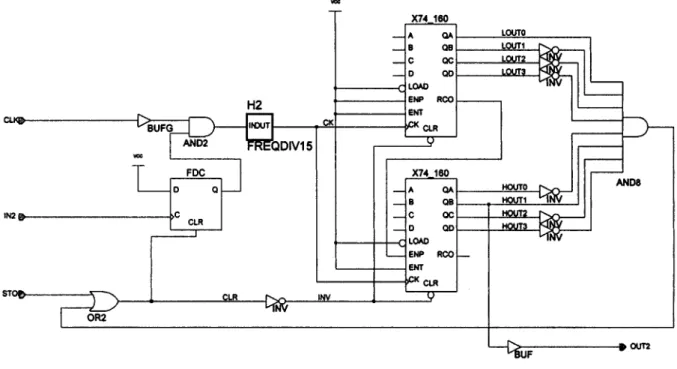
3. Timed transition. It denotes event transfer with delay time t. As shown in Figure 4, it is implemented by a timer with delay time t and start–reset functions. The timer output becomes high at t time later than the arrival of a logic high signal at the timer input. To achieve this function, a two-level hierarchy configuration circuit is used. The lower level is a frequency divider, namely FREQDIV15 in this study, dividing the input clock frequency by 15. The FREQDIV15 circuit is shown in Figure5, where the X74 160
is a 4-bit BCD counter [11]. The FREQDIV15 sends a clock pulse out for every 15 input clock pulses and clears X74 160 at the positive edge of the 16th clock pulse. The FREQDIV15 is generated to a macro symbol, as shown in Figure 6, for the design toolbox of this project file. The upper-level circuit of the timer configuration is shown in Figure 6. There is an existing oscillator in Xilinx XACT libraries, namely OSC4, which supplies five different frequencies of clock, i.e. 15 Hz, 490 Hz, 16 kHz, 500 kHz and 8 MHz. The FREQDIV15 outputs a 1 Hz clock by feeding the OSC4 15 Hz clock into the FREQDIV15. The 1 Hz clock is used as a time-base to generate the N -second time delay for timed transition and merely lets the FREQDIV15 follow a MOD-N frequency divider. A MOD-20 frequency divider circuit, for example, follows the FREQDIV15 in Figure6. The D flip-flop and the AND gate construct a switch to start and stop counting delay time of timed transitions by the IN2 trigger signal and the STOP signal respectively. The STOP signal also resets the timer. Using the technique similar to the DELAY20 and the five clock frequencies provided by OSC4, a variety of delay times can be implemented.
106 S. K. YANG AND T. S. LIU
Figure 6. Circuit of DELAY20
Figure 7. Early failure detection and isolation arrangement (EFDIA)
4. EXAMPLE
The early failure detection and isolation arrangement (EFDIA) depicted in Reference [7] and shown in Figure7is employed in this section to exemplify the realization of Petri nets using an FPGA. All necessary components have been constructed in Section3.
4.1. Circuit of EFDAI
Using circuits described in Section 3, the logic circuit of the EFDIA is constructed as shown in Figure8. Each of H3 and H4 in Figure8 is a timer composed of DELAY20. The EFDIA circuit can be integrated into a 39-pin ASIC. Figure 9 shows the macro symbol for EFDIA. Hence the EFDIA Petri net is realized to become an ASIC after downloading this EFDIA macro to a Xilinx FPGA board.
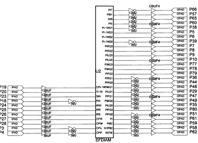
The correspondence between EFDIA pin names (Figure 9) and EFDIA Petri net symbol names (Figure7) is listed below.
1. Input pins
(1) CPI-1W: clear signal, which is implicit in Figure14, for Next Lower PWcounter (2) TI-1S: Next Lower TS
(3) SIN: Si
(4) PIA: PAi
(5) IRW: ith Reset W (6) IRR: ith Reset R (7) IRE: ith Reset E
(8) CPIR: clear signal, which is implicit in Figure14, for PR
i counter
(9) CPIM: clear signal, which is implicit in Figure14, for PMi counter
(10) CPIL: clear signal, which is implicit in Figure14, for PLi counter
IMPLEMENTATION OF PETRI NETS 107 F igure 8 . C ircuit of E F D IA
108 S. K. YANG AND T. S. LIU
Figure 9. EFDIA macro symbol
(11) CPIF: clear signal, which is implicit in Figure14, for PFi counter
2. Output pins
(1) PIT: PTi (2) PIB1: PB1i
(3) IWS: ith WARNING SIGNAL (4) PIE: PEi
(5) PI-1WQ0–PI-1WQ3: Next Lower PW counter (6) PIRQ0–PIRQ3: PRi counter (7) PILQ0–PILQ3: PLi counter (8) PIFQ0–PIFQ3: PFi counter (9) PIMQ0–PIMQ3: PMi counter (10) PI: Pi (11) PIB2: PB2i (12) NHPB2: Next Higher PB2 (13) ASFM: ASFM
4.2. Simulations for EFDIA
To verify the EFDIA logic circuit, i.e. Figure 8, the following three failure scenarios are simulated.
These simulations are all performed on a Xilinx Logic Simulator.
4.2.1. The TI-1S is low and the PIA is high. This simulation accounts for the case where the error signal is not caused by the next lower subsystem (module) and PM action for the malfunctioning subsystem (module) takes place in time. The resultant timing diagram for this simulation is shown in Figure 10, which is generated by a Xilinx Wave Viewer. A logic high signal is sent to the SIN by the simulator, which indicates that the monitored signal of the ith place exceeds the prescribed warning value. Subsequently, each of PIB1, NHPB2, IWS and PIT is triggered. The H4 timer, whose output is the H4OUT2 as shown in Figure 6, starts counting. The delay time of the H4 timer, which is denoted by TiU in Figure 7,
represents the time between the warning value and the maximum allowed value for system performance, i.e. the maintenance lead time [7]. If the PM action is taken before the system failure occurs, i.e. before the H4 timer completes counting, the PIA sends a signal to start the H3 timer and to stop the H4 timer at the same time. The delay time of the H3 timer
IMPLEMENTATION OF PETRI NETS 109
represents the time for the PM action to complete. As shown in Figure10, for example, the PIA signal arises at the seventh count of the H4 timer. Owing to the inhibition configuration of TiUtransition, which is
constructed by the ith WARNING SIGNAL and the PAi , TIU will not be triggered because the H4 timer stops counting once the PIA is high. Hence PI remains low from the beginning to the end of this case, i.e. the system failure is avoided. The output signal of the H3 timer is the H3OUT2 in Figure10. After H3 counts 20, i.e. after the correcting work for the system error is completed, the PIM counter is triggered such that the PIMQ0 becomes one. At the same time the SIN becomes low and each of PIB1, NHPB2, IWS and PIT in turn becomes low. On the other side of the EFDIA, since PIB2 is low and PIB1 is high, TIE becomes high, which triggers the PIL counter such that the PILQ0 becomes one when IRE generates a trigger signal. Consequently, the error time log number of the
ith subsystem increases by one. Since PIE is the error
indication flag for the EFDIA, PIE high indicates that the error signal is from the ith subsystem but not the next lower one. The PIE timing curve is shown at the bottom in Figure10.
4.2.2. The TI-1S is high and the PIA is high.
This simulation deals with an error signal arising from the next lower subsystem but not the ith subsystem itself. The timing diagram for this simulation is shown in Figure11. Owing to logic relations constrained by the Petri net dealing with system failures [12], the SIN becomes high after the high TI-1S signal. The high SIN signal triggers each of PIB1, NHPB2, IWS and PIT to become high. The H4 timer is triggered to count by low PIA and high IWS. The low PIE indicates that the error is not located in the ith subsystem itself. Triggering the IRW enables the PI-1WQ0 to become one. Hence the warning time log number of the next lower subsystem increases by one. Since the PIE is low, the PIRQ0 can be triggered by an IRR signal and high PIB1. In this simulation the PIA signal triggers the H3 timer to count after an inspection for the ith subsystem but not a maintenance action. Once the H3 timer starts counting, the H4 timer counting stops. When the PIMQ0 becomes one, i.e. the maintenance log number of the ith subsystem increases by one, the SIN resumes low from high. The TI-1S resets to low after the correcting work for the next lower subsystem is completed. The PI signal remains low in this simulation, i.e. a Pifailure never occurs.
4.2.3. The TI-1 is low and the PIA is low. This last simulation accounts for error existing in the ith
subsystem but without PM. The PIE is triggered to high by high PIB1 and low PIB2. High PIE implies that the error is located in the ith subsystem. The H4 timer is triggered to count by the warning signal IWS and low PIA. Since the PM action is not taken during the maintenance lead time, i.e. the delay time of the H4 timer, the PIU becomes high after the H4 timer counts 20. As a result, the PI becomes high, representing Pi
failure occurring. The failure time log number of this subsystem increases by one, i.e. the PIFQ0 becomes one at this moment. The PILQ0 is also triggered by the IRE signal to increase the error time log number by one for the ith subsystem. The timing diagram for this simulation is shown in Figure12.
4.3. Implementation
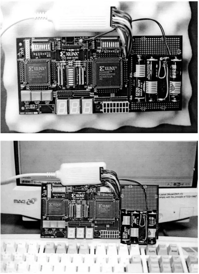
The EFDIA logic circuit is implemented by downloading its schematic diagram to a Xilinx FPGA Demonstration Board. The board is a stand-alone board for experimenting and developing prototypes using the Xilinx FPGA architecture. Two FPGA devices, namely XC3020A and XC4003E, have been installed on the board. The XC4003E has higher density and more input/output blocks and flip-flops than the XC3020A [6]. Hence the XC4003E is adopted in this study to implement the EFDIA. The configuration of the XC4003E for implementing the EFDIA is described as follows.
1. Power supply. The power for the Demonstration Board is supplied by a battery set, which has three AA (UM-3) batteries in series to supply +5 V through the connector J9 of the board.
2. Downloading interface. The EFDIA schematic diagram for configuring the XC4003E is down-loaded from a personal computer through an Xchecker cable [13] which connects either the COM1 or COM2 port of the computer to the J2 connector of the board.
3. Input terminals. Switches SW3, SW4 and SW5 provide input signals for the XC4003E to implement the EFDIA circuits. The SW3 is a switch set with eight switches connecting to eight general-purpose inputs on XC4003E input pins. An XC4003E input pin is set to logic 1 when the corresponding switch is on and to logic 0 when the corresponding switch is off. The SW4, namely Reset Pushbutton, can apply an active-Low reset signal to the XC4003E via pin 56 when the SW2-7 switch is on. The SW5, namely Spare Pushbutton, also applies an active-Low signal to the XC4003E via pin 18.
110 S. K. YANG AND T. S. LIU F igure 10. T im ing diagram for ‘T I-1S is lo w and P IA is high’ si m u lation
IMPLEMENTATION OF PETRI NETS 111 F igure 11. T im ing diagram for ‘T I-1S is h igh and P IA is h igh’ si m u lation
112 S. K. YANG AND T. S. LIU F igure 12. T im ing diagram for ‘T I-1S is lo w and P IA is lo w ’ si m u lation
IMPLEMENTATION OF PETRI NETS 113
114 S. K. YANG AND T. S. LIU F igure 14. I/O as si gnm ent o f D em ons tration B oard for E F D IA im p lem entation
IMPLEMENTATION OF PETRI NETS 115
4. Output terminals. Three seven-segment displays are included, with the U6 connecting to the XC3020A and the U7 and U8 connecting to the XC4003E. Each LED segment is turned on by driving the corresponding FPGA pin Low with logic 0. Decimal points serve as state and error indicators. Besides, there are eight LEDs connected to the I/O pins in each FPGA. LEDs D1–D8 connect to the XC3020A, while D9–D16 connect to the XC4003E. Each LED is also turned on by driving its corresponding FPGA pin Low with logic 0. There are 16 extra I/O lines that connect each FPGA.
Figure 13 shows two pictures of the downloaded Demonstration Board. The I/O assignment on the Demonstration Board for the EFDIA implementation is shown in Figure14.
4.4. Results
According to timing diagrams for the simulations in Section 4.2, i.e. Figures 10–12, and operations on the downloaded Demonstration Board, the EFDIA logic circuit functions identically to the EFDIA Petri net. All the capabilities of the EFDIA Petri net, including alarm, early failure detection, fault isolation, event count, system state description and automatic shutdown or regulation, are preserved in the 39-pin ASIC depicted in Section4.1. Hence the Petri net has been realized by FPGA circuits.
5. APPLICATIONS
The capabilities of the EFDIA are very useful for health monitoring, on-line failure prognostics and preventive maintenance of a system. No matter what scale the system is, the EFDIA is applicable. From large systems such as power plants and chemical plants to smaller systems such as automobiles and machinery, a set of personal computers, or a CD-ROM, is within the scope of EFDIA application. Taking an automobile as an example, a warning light shown on the panel denotes that a failure with prescribed threshold is going to occur and where the cause comes from, by equipping an EFDIA ASIC to each of the sensing points corresponding to places in the Petri net. Consequently, errors in an automobile can be corrected before a failure occurs by preventive maintenance. Accordingly, driving safety can be ensured.
6. CONCLUSIONS
Although Petri nets are suitable to perform modelling, analysis, verification, reduction, synthesis and so on, the Petri net approach is done on paper. Since Petri nets are state machines, however, they can be designed to perform those capabilities. This paper has presented a hardware implementation of Petri nets, including basic symbols, basic logic structures and specific functions for Petri nets. Besides, the Petri net with early failure detection and isolation functions has been implemented as a 39-pin ASIC on a Xilinx Demonstration Board as an example. This ASIC was verified by three simulations dealing with three different failure scenarios of a system. The 39-pin ASIC functions identically to the EFDIA Petri net. Since Petri nets offer a convenient modelling paradigm and various other functions, not only the EFDIA Petri net but also any specific function Petri nets can be implemented by FPGA circuits.
REFERENCES
1. Shaw AW. Logic Circuit Design; Fort Worth Saunder College Publishing: Fort Worth, TX, 1993.
2. Roth Jr. CH. Fundamentals of Logic Design, (4th edn); International Thomson Publishing: Taipei, 1995.
3. Chang N, Kwon WH, Park J. FPGA-based implementation of synchronous Petri nets. Proceedings of the IECON’96 International Conference on Industrial Electronics, Control, and Instrumentation, 1996; pp. 469–474.
4. Peterson JL. Petri Net Theory and the Modeling of Systems; Prentice-Hall: Englewood Cliffs, NJ, 1985; pp. 166–172. 5. Stefano AD, Mirabella O. A fast sequence control device
based on enhanced Petri nets. Microprocessors and Microsys-tems 1991; 15:179–186.
6. CIC. Training Course 12; Chip Implementation Center of Nation Science Council: Taipei, 1998.
7. Yang SK, Liu TS. A Petri net approach to early failure detection and isolation for preventive maintenance. Quality and Reliability Engineering International 1998; 14:319–330. 8. Schroeter J. Surviving the ASIC Experience; Prentice-Hall:
Englewood Cliffs, NJ, 1992.
9. Xilinx. Foundation Series Quick Start Guide Version F1.4; The Programmable Logic Company: San Jose, CA, 1998. 10. David R, Alla H. Petri nets for modeliing of dynamic
systems—a survey. Automatica 1994; 30:175–202.
11. Xilinx. XACT Libraries Guide; The Programmable Logic Company: San Jose, CA, 1994.
12. Yang SK, Liu TS. Failure analysis for an airbag inflator by Petri nets. Quality and Reliability Engineering International 1997; 13:139–151.
13. Xilinx. Hardware User Guide; The Programmable Logic Company: San Jose, CA, 1998.
Authors’ biographies:
S. K. Yang was born in Taiwan. He received his BS and MS in automatic control engineering from Feng Chia University, Taiwan in 1982 and 1985 respectively. From 1985 to 1991 he was an assistant researcher and
116 S. K. YANG AND T. S. LIU
instrumentation system engineer of Flight Test Group, Aeronautic Research Laboratory, Chung Shan Institute of Science and Technology, Taiwan. Since 1991 he has been with the Department of Mechanical Engineering at National Chin Yi Institute of Technology, Taiwan where he is currently an associate professor. He received his PhD in mechanical engineering from National Chiao Tung University, Taiwan in 1999. His research interests are in reliability, data acquisition and automatic control.
T. S. Liu received his BS from National Taiwan University in 1979 and MS and PhD from the University of Iowa, USA in 1982 and 1986 respectively, all in mechanical engineering. Since 1987 he has been with the National Chiao Tung University, Taiwan where he is currently a professor. From 1991 to 1992 he was a visiting researcher at the Institute of Precision Engineering, Tokyo Institute of Technology, Japan. His current research interests include reliability, design and motion control.