國立交通大學
電子工程學系 電子研究所碩士班
碩 士 論 文
長脈衝傳輸線觸波技術及其在
積體電路電纜放電防護上之應用
LONG-PULSE TRANSMISSION LINE
PULSING TECHNIQUE FOR CABLE
DISCHARGE EVENT (CDE) PROTECTION
IN CMOS INTEGRATED CIRCUITS
研究生 : 賴 泰 翔
指導教授 : 柯 明 道 教授
中華民國九十五年七月
長脈衝傳輸線觸波技術及其在
積體電路電纜放電防護上之應用
Long-Pulse Transmission Line Pulsing Technique for
Cable Discharge Event (CDE) Protection in CMOS
Integrated Circuits
研 究 生: 賴泰翔
Student : Tai-Hsiang Lai
指導教授: 柯明道 教授
Advisor : Prof. Ming-Dou Ker
國立交通大學
電子工程學系 電子研究所碩士班
碩士論文
A Thesis
Submitted to Department of Electronics Engineering & Institute of Electronics
College of Electrical and Computer Engineering
National Chiao-Tung University
in Partial Fulfillment of the Requirements
for the Degree of
Master
in
Electronics Engineering
July 2006
Hsinchu, Taiwan, Republic of China
長脈衝傳輸線觸波技術及其在
積體電路電纜放電防護上之應用
學生: 賴泰翔 指導教授: 柯 明 道 教授
國立交通大學
電子工程學系 電子研究所碩士班
ABSTRACT (CHINESE)
摘要
電纜放電(Cable Discharge Event, CDE)已是造成網路介面積體電路損傷的主 要原因。而在靜電放電(Electrostatic Discharge, ESD)防護元件之耐受能力測試 中,傳輸線脈衝產生系統(Transmission Line Pulsing System, TLP)是觀測元件在靜 電轟擊下電性特徵最重要的方法。一方面為了解電纜放電防護元件之物理特性, 另一方面更能在晶片製作完成之初,能先了解產品之電纜放電的承受能力。於是 本篇論文利用架設的長脈衝傳輸線脈衝產生系統去模擬電纜放電對測試元件的 影響,並用來量測和分析電纜放電防護元件之二次崩潰特性,然後再與傳統的傳 輸線脈衝產生系統進行比較。透過新提出的長脈衝傳輸線脈衝系統(Long-Pulse Transmission Line Pulsing System, LP-TLP)和傳統的傳輸線脈衝產生系統對元件 進行測試後,發現元件對電纜放電耐受度比起人體放電模式(Human Body Model, HBM)靜電放電耐受度明顯降低。 在本論文中,由電纜放電防護基本元件在遭到電纜放電衝擊下啟動的基本原 理為起點,實際在0.25 微米及 0.18 微米互補式金氧半製程中,以變化不同的佈 局參數,來改變指狀結構(Finger-Type)之電纜放電防護基本元件的佈局結構,利 用 長 脈 衝 - 傳 輸 線 脈 衝 系 統 量 測 到 之 待 測 元 件 的 二 次 崩 潰 點(Secondary Breakdown Point),來說明及探討元件佈局結構對電纜放電耐受力的影響,並由 長脈衝傳輸線脈衝系統之測試結果中,得到最佳化的佈局方式和佈局參數。並在
待測元件經由傳輸線脈衝系統與長脈衝傳輸線脈衝系統測試後,利用掃描電子顯 微鏡(Scanning Electron Microscope, SEM)觀察閘極接地 N 型金氧半場效電晶體 (Gate-Ground NMOS, GGNMOS)的故障分析照片,進一步分析電纜放電耐受度比 起人體放電模式靜電放電耐受度明顯降低之主要原因。
比起其他的靜電放電防護元件,例如二極體(Diode)、雙載子電晶體(BJT)、 金氧半場效電晶體(MOSFET)、或場氧化層電晶體(Field Oxide Device, FOD),由 於矽控制整流器(Silicon Controlled Rectifier, SCR)具有較低的持有電壓(Holding Voltage),所以其具有較高的靜放放電防護能力。於是本論文利用提出的長脈衝 -傳輸線脈衝系統測試橫向矽控制整流器(Lateral Silicon Rectifier, LSCR)及修改 的橫向矽控制整流器(Modified Lateral Silicon Rectifier, MLSCR)是否依然具有高 的電纜放電防護能力,經測試後發現不管是橫向矽控制整流器或者是修改的橫向 矽控制整流器皆具有高的電纜放電耐受能力。 此外,由於電纜線在插拔多次後,也可能造成電纜數據機或乙太網路積體電 路的損傷。因此,本論文首先提出利用長脈衝傳輸線脈衝技術去模擬此不同的電 纜放電現象,結果發現此電纜放電現象仍然會引起一般的靜電放電防護元件-閘 極接地N 型金氧半場效電晶體,從其中一個指狀的汲極(Drain)燒到源極(Source) 的毀壞情況。所以,此類的電纜放電對乙太積體電路可靠度也是一嚴重的威脅, 值得相關產業或研究單位去重視它並提出有效的設計解決方案。
LONG-PULSE TRANSMISSION LINE
PULSING TECHNIQUE FOR CABLE
DISCHARGE EVENT (CDE) PROTECTION
IN CMOS INTEGRATED CIRCUITS
Student: Tai-Hsiang Lai Advisor: Prof. Ming-Dou Ker
Department of Electronics Engineering & Institute of Electronics
National Chiao-Tung University
ABSTRACT (ENGLISH)
ABSTRACT
Cable discharge event (CDE) has been the main cause which damages the Ethernet interface. The transmission line pulsing (TLP) system has been the most important method to observe the electric characteristics of the device under human-body-model (HBM) ESD stress. To understand the physical characteristics and CDE robustness of protection device in the wafer level, the long-pulse transmission line pulsing (LP-TLP) system has been set up and used to simulate the influence of CDE on the Ethernet integrated circuits and to measure and analyze the secondary breakdown characteristics of the CDE protection devices. Furthermore, the measured results by using the LP-TLP system are compared with those by using the traditional 100-ns TLP system. The experimental results have shown that the CDE robustness of NMOS and PMOS devices in deep-submicron CMOS technology is much worse than their HBM ESD robustness.
In order to realize the turn-on mechanisms of CDE protection devices during CDE stress, the turn-on characteristics of those devices must be measured and analyzed in this thesis. The LP-TLP measurement and the Scanning Electron Microscope (SEM) photographs have been used to analyze and explain the physical turn-on mechanisms of CDE protection devices. From the investigation of layout dependence on CDE robustness of gate-grounded NMOS (GGNMOS) and gate-VDD PMOS (GDPMOS) with finger-type layout, the turn-on mechanisms of CDE protection devices can be clearly understood to optimize the layout rules for the device dimensions, the layout style, and the layout spacings of those devices. To design high performance CDE protection device, some layout parameters must be optimized. The optimal layout parameters in both 0.25-μm and 0.18-μm salicided CMOS technologies have been clearly investigated and analyzed. Moreover, from the SEM photographs of GGNMOS device to observe the failure locations after the traditional TLP and the proposed LP-TLP tests, the reason for an evident reduction on the It2 of GGNMOS device under CDE stress can be further studied.
Due to the low holding voltage (Vhold, about ~1.5 V in general CMOS process)
of silicon controlled rectifier (SCR) device, the power dissipation (power = IESD×Vhold)
located on the SCR device during ESD stress is significantly less than that located on other ESD protection devices, such as the diode, BJT, MOS, or field-oxide device. The SCR device can sustain a much higher ESD level within a smaller layout area in CMOS ICs, so it has been effectively used to protect the internal circuit against ESD damages for a long time. Thus, the CDE robustness of lateral SCR (LSCR) and modified lateral SCR (MLSCR) devices can be measured and investigated by the proposed LP-TLP technique to check them whether the SCR devices can sustain a higher CDE capability. From the experimental results, the LSCR and MLSCR devices
can still possess higher CDE levels.
In additional, Multiple CDE events occur when cable with some charges is plugged in and pulled out many times. This event can lead the cable modems, the Ethernet interfaces and the video equipments to be damaged. Therefore, this issue can be experimentally investigated in more detail by applying the LP-TLP system with fixed low zapping energy but multiple zapping times. From the failure analysis, a GGNMOS device, which ha been widely used as the on-chip ESD protection device in CMOS ICs, is directly burned out from drain to source in one finger after such CDE stress. So, such CDE-induced stress is also a crucial reliability challenge in Ethernet integrated circuits.
誌謝
ACKNOWLEDGEMENT
首先,我要感謝我的指導教授柯明道博士,這兩年來給我的耐心指導和鼓 勵,使我能順利完成碩士學業。還記得碩一剛進實驗室時,在做研究上是個搞不 懂狀況的菜鳥,跌跌撞撞,胡亂摸索,報告時常被教授火力全開,那時覺得很辛 苦、很挫折,但也是我成長最迅速的時候。現在回想起來,心中只有萬分感激, 而無一絲的抱怨。「做事要有效率,研究要有成果。」是教授在 meeting 時,常 對我們group 說的一句話。我會稟持此一精神與態度在未來的研究、工作上繼續 努力。 在這段求學的過程中,感謝實驗室的學長們對我的指導和協助,尤其是林昆 賢、陳世倫、鄧志剛、徐新智、許勝福、陳榮昇、顏承正、張偉仁、陳世宏、蕭 淵文和王暢資諸位學長們,在 ESD 的電路設計和實驗量測方面給我許多寶貴意 見和指導。此外,感謝工研院張伯瑋學長以及曾任職於工研院的張智毅學長和陳 子平學長在實驗上的幫忙。也感謝實驗室助理卓慧貞小姐在實驗室行政事務上的 許多協助。 謝謝同年級的戰友們,怡凱、豪傑、志遠、汝玉、允斌、仲朋、必超、資閔、 芳綾、佳惠、宛儀、立龍、國慶、志賢,大家一起修課、做研究、熬夜,一起打 球、出遊、唱歌、談心,休憩與共,讓我的研究生生活多采多姿。 此外,碩二下學期至聯電實習時,公司的學長姐們,尤其是唐天浩經理、趙 美玲學姐、吳俊毅學長、黃致遠學長、黃新言學長、廖萌慧學姐、柯鈞鐘、陳韋 如,給我很多工作和研究上的幫忙,讓我在實習期間,又充實了不少,在此也一 併感謝。 最後,我要致上最深的感謝給予我的奶奶賴鄧細悌女士、父親賴金水先生、 母親黃勤芳女士、妹妹欣臨,一直以來對我永無止境的付出、鼓勵、支持與照顧, 讓我能專心在課業研究上學習,在此由衷地感謝你們。另外,要祝福所有在這兩 年間與我相處過的師長、朋友、學弟妹們,有緣與你們同在這一個階段成長,是 我一生的榮幸,願大家都能順心如意、心想事成! 賴 泰 翔 謹誌於竹塹交大 九十五年 六月CONTENTS
ABSTRACT (CHINESE) ... i
ABSTRACT (ENGLISH)...iii
ACKNOWLEDGEMENT ... vi
CONTENTS ... vii
TABLE CAPTIONS ... ix
FIGURE CAPTIONS ... x
Chapter 1 Introduction ... 1
1.1 BACKGROUND...1 1.2 THESIS ORGANIZATION...2Chapter 2 Cable Discharge Test ... 5
2.1 CDE IN ETHERNET LOCAL AREA NETWORK...5
2.2 DISCHARGE BETWEEN LANCABLING AND EQUIPMENT...6
2.3 SUMMARY...7
Chapter 3 Long-Pulse TLP (LP-TLP) Measurement Setup 13
3.1 TRADITIONAL TRANSMISSION LINE PULSING (TLP)SYSTEM...133.2 NEW LONG-PULSE TRANSMISSION LINE PULSING (LP-TLP)SYSTEM..13
3.2.1 Measurement setup of the proposed LP-TLP...13
3.2.2 Verification on LP-TLP with a Load of 50-Ω Resistor ...15
3.2.3 Verification on Gate-Grounded NMOS (GGNMOS) ...15
3.3 SUMMARY...16
Chapter 4 Dependence of Layout Parameters on CDE
Robustness of CMOS Devices ... 25
4.1.1 Channel Width...26
4.1.2 Channel Length...27
4.1.3 Unit-Finger Width ...28
4.1.4 Spacing from Source Contact to Poly-Gate Edge...29
4.1.5 SAB Width ...30
4.1.6 Failure Analysis ...31
4.2 NMOS/PMOS IN A 0.18-μmSALICIDED CMOSPROCESS...32
4.2.1 Clearance from SAB to Poly-Gate Edge...32
4.2.2 Distance from drain diffusion to Guard Ring Edge ...33
4.3 COMPARISON BETWEEN 0.25-μm AND 0.18-μmCMOSPROCESSES...34
4.4 SCRDEVICE IN A 0.18-μm CMOSPROCESS...35
4.4.1 Lateral SCR (LSCR)...36
4.4.2 Modified Lateral SCR (MLSCR)...37
4.5 APPLICATION OF LP-TLPSYSTEM...38
4.6 SUMMARY...41
Chapter 5 Conclusions and Future Works ... 60
5.1 MAIN RESULTS OF THIS THESIS...60
5.2 FUTURE WORKS...61
REFERENCES ... 62
VITA 64
TABLE CAPTIONS
Table 2.1 The descriptions for process technologies and IC designs of different types of
Ethernet transceivers...8
FIGURE CAPTIONS
Fig. 1.1 The Ethernet interface is damaged by CDE event. ...4
Fig. 2.1 The test setup used to measure and analyze CDE in an Ethernet network [3], [4]...9
Fig. 2.2 The CDE voltage levels of Ethernet transceivers under different IC designs and process technologies [3], [4]. ...9
Fig. 2.3 Cable layout of unshielded twisted pair (UTP) [5, [6]...10
Fig. 2.4 Charging point [6]...10
Fig. 2.5 Discharging point [5], [6]... 11
Fig. 2.6 Cable discharge waveforms when (a) unused pairs connected together and grounded and (b) unused pairs floating [5]...12
Fig. 3.1 The measurement setup for the traditional TLP test. ...18
Fig. 3.2 The 100-ns TLP current waveforms on a 50-Ω resistor under different charged voltages...18
Fig. 3.3 The measurement setup for the proposed LP-TLP test...19
Fig. 3.4 The actual measurement setup for the proposed LP-TLP test. ...19
Fig. 3.5 The (a) 500-ns and (b) 1000-ns LP-TLP current waveforms on a 50-Ω resistor under different charged voltages...20
Fig. 3.6 The 500-ns LP-TLP measured I-V characteristic of GGNMOS device. ...21
Fig. 3.7 (a)-(f) The measured time-domain I-V waveforms of GGNMOS device at the corresponding points marked in Fig. 3.6. ...22
Fig. 3.8 The 1000-ns LP-TLP measured I-V characteristic of GGNMOS device. ...23
Fig. 3.9 (a)-(f) The measured time-domain I-V waveforms of GGNMOS device at the corresponding points marked in Fig. 3.8. ...24
Fig. 4.1 The layout top view of finger-type GGNMOS device with different layout parameters...43
Fig. 4.2 The 500-ns LP-TLP measured I-V characteristics and the leakage currents of the GGNMOS devices with different channel widths. ...43
Fig. 4.3 The dependence of the It2 of (a) GGNMOS and (b) GDPMOS devices on the channel width under the traditional 100-ns TLP and the proposed 500-ns (1000-ns) LP-TLP tests...44
Fig. 4.4 The dependence of the It2 of (a) GGNMOS and (b) GDPMOS devices on the channel length under the traditional 100-ns TLP and the proposed 500-ns (1000-ns) LP-TLP tests...45
Fig. 4.5 The dependence of the It2 of (a) GGNMOS and (b) GDPMOS devices on the
(1000-ns) LP-TLP tests...46
Fig. 4.6 The dependence of the It2 of (a) GGNMOS and (b) GDPMOS devices on the
spacing from source contact to poly-gate edge under the traditional 100-ns TLP and the proposed 500-ns (1000-ns) LP-TLP tests. ...47
Fig. 4.7 The dependence of the It2 of (a) GGNMOS and (b) GDPMOS devices on the
SAB width under the traditional 100-ns TLP and the proposed 500-ns (1000-ns) LP-TLP tests...48
Fig. 4.8 SEM photographs on the GGNMOS device (W/L=420μm/0.3μm) to observe
its failure locations after (a) the traditional 100-ns TLP test, (b) the proposed 500-ns LP-TLP test, and (c) the proposed 1000-ns LP-TLP test...49
Fig. 4.9 The dependence of the It2 of (a) GGNMOS and (b) GDPMOS devices on the
clearance from SAB to poly-gate edge under the traditional 100-ns TLP and the proposed 500-ns (1000-ns) LP-TLP tests. ...50
Fig. 4.10 The dependence of the It2 of GGNMOS device on the distance from drain
diffusion to guard ring edge under the traditional 100-ns TLP and the proposed 500-ns (1000-ns) LP-TLP tests. ...51
Fig. 4.11 The relations between (a) the channel width (b) the channel length and the
It2 of GGNMOS device under the 500-ns LP-TLP stress in both 0.25-μm and 0.18-μm CMOS technologies. ...52
Fig. 4.12 The device structure of the lateral SCR (LSCR) in CMOS process. ...53 Fig. 4.13 The measured I-V characteristics of the LSCR device under the traditional
100-ns TLP and the proposed 500-ns (1000-ns) tests in a 0.18-μm CMOS process...53
Fig. 4.14 The device structure I of the modified lateral SCR (MLSCR) in CMOS
process...54
Fig. 4.15 The measured I-V characteristics of the MLSCR structure I under the
traditional 100-ns TLP and the proposed 500-ns (1000-ns) tests in a
0.18-μm CMOS process. ...54
Fig. 4.16 The device structure II of the modified lateral SCR (MLSCR) in CMOS
process...55
Fig. 4.17 The measured I-V characteristics of the MLSCR structure II under the
traditional 100-ns TLP and the proposed 500-ns (1000-ns) tests in a
0.18-μm CMOS process. ...55
Fig. 4.18 Comparison of 500-ns LP-TLP with 100-ns TLP for a GGNMOS device
with W/L=240μm/0.25μm fabricated in 0.18-μm CMOS process...56
Fig. 4.19 The profile for the energy of zaps (%) versus number of zaps to failure
relationship under the 500-ns LP-TLP and 100-ns TLP stresses...56
under I_LP-TLP=90%´It2 stress...57
Fig. 4.21 The measured DC I-V curves of GGNMOS device (W/L=240μm/0.25μm)
with applied voltage at (a) drain node, and (b) source node, under different stress conditions...58
Fig. 4.22 SEM pictures on the GGNMOS device to observe its failure conditions after
500-ns LP-TLP stress of (a) continuously zapping with increasing energy to fail, and (b) repeatedly zapping with fixed 90% energy to fail. ...59
Chapter 1
Introduction
1.1 B
ACKGROUNDCable Discharge Event (CDE) is a critical reliability issue that requires recognition at all levels in the networking industry. The characteristics of twisted-pair cable in different environments play an important role in CDE event. Frequently changing cable environments also increase the challenge of preventing CDE event. With more understanding on CDE characteristics and discharge waveforms, the designers can achieve the best protection against CDE event through a good chip layout skill and a careful selection of on-chip protection components.
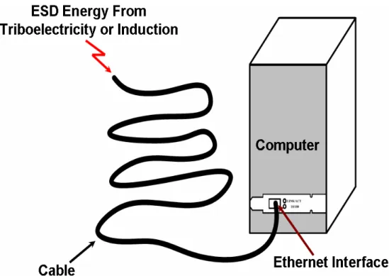
Electrostatic charges accumulate on a cable primarily through triboelectric (friction) effects or electromagnetic induction. For instance, the friction will result in accumulated charges as a cable is dragged across a floor or through the conduit. The positive tribo-charges on the outside surface of the cable attract negative charges in the twisted pair across the dielectric region, and then sweep the induced positive charges to the ends of the cable. Note that there is no net charge in the twisted-pair cable. Electromagnetic induction effects can be observed when cable accumulates charges from adjacent electromagnetic field. CDE event is similar to the electrostatic discharge (ESD) event that happens when the cable filled with accumulated charges is plugged into the Ethernet interface or the electronic equipments. However, unlike the human-body-model (HBM) which is a very high impedance and low capacitance model, CDE can discharge a very large amount of charges with low impedance. This means that CDE event will lead much more energy to be absorbed by the
semiconductor devices than HBM ESD event. So, such high-energy discharge of CDE event could damage the connectors, the electronic equipments, and the Ethernet interfaces that are designed to withstand HBM ESD discharges. This CDE phenomenon is illustrated in Fig. 1.1. Some international corporations or organizations have started to discuss such CDE issues [1]-[7]. Most CMOS IC products are routinely tested by following the EIA/JEDEC Standard No.78 [8] to evaluate their latchup robustness. However, the CDE-induced latchup is a more severe condition [1]. Currently, there is no established component-level standard for CDE tests [3], [4]. In this thesis, the long-pulse transmission line pulsing (LP-TLP) system is proposed as the efficient measurement method to investigate the CDE reliability of IC products.
1.2 T
HESISO
RGANIZATIONThe chapter 2 of the thesis introduces and discusses two kinds of the typical cable discharge tests. One is to investigate the CDE robustness in Ethernet local area network (LAN), and another one is to measure CDE discharge waveforms of unshielded twisted pair (UTP) cables. The first kind of test result reveals how the effects of CDE can be minimized through process technology and IC design. From the second kind of test result, the pulse widths of all discharge currents of these UTP cables are approximately ~475 ns. This pulse width provides us a way to find the efficient component-level measurement method for investigating CDE robustness of I/O devices in IC products.
In the chapter 3, a new long-pulse transmission line pulsing (LP-TLP) system is proposed and set up. The proposed LP-TLP system with two kinds of long pulse widths (500 ns/1000 ns) is evidently different from the traditional TLP system with a
short pulse width of 100 ns. The LP-TLP system with a pulse width of 500 ns is consistent to the pulse width (~475 ns) of CDE in Fig. 2.6. Therefore, the LP-TLP system can be utilized to examine the damage situation on the DUT under CDE stress.
In the chapter 4, the dependence of different layout factors on the CDE level of the gate-grounded NMOS (GGNMOS) and gate-VDD PMOS (GDPMOS) are practically investigated through fabricated silicon chips in both 0.25-μm and 0.18-μm salicided CMOS processes. To clearly understand the difference between the CDE level and the HBM ESD level, the proposed LP-TLP and the conventional TLP measured data are compared to find the dependence on layout parameters. The silicon controlled rectifier (SCR) device can sustain a much higher ESD level within a smaller layout area in CMOS ICs, so it has been effectively used to protect the internal circuit against ESD damages for a long time. In order to understand it whether the SCR device can bypass high CDE current,the CDE robustness of lateral SCR (LSCR) and modified lateral SCR (MLSCR) devices can be measured and investigated by the proposed LP-TLP technique. From the experimental results, the LSCR and MLSCR devices can still sustain higher CDE levels. Furthermore, Multiple CDE events occur when cable with some charges is plugged in and pulled out many times. This event can lead the cable modems, the Ethernet interfaces and the video equipments to be damaged. Therefore, this issue can be experimentally investigated in more detail by applying the LP-TLP technique with fixed low zapping energy but multiple zapping times.
Chapter 2
Cable Discharge Test
2.1 CDE
INE
THERNETL
OCALA
REAN
ETWORKIn order to investigate the CDE robustness in Ethernet local area network (LAN), a test setup was proposed in Fig. 2.1 [3], [4]. First, a standard category-5 cable was connected to an Ethernet transceiver and then an unterminated category-6 cable was charged in 500-V increments starting at 1kV by ESD gun. Afterward, the patch cable was inserted directly into the patch panel to examine the CDE robustness of Ethernet transceivers. An Ethernet transceiver was “failed” if its transmit signal amplitude degraded by more than 10 %, so it was unable to link, or it experienced destructive latchup.
By utilizing the test setup and procedure in Fig. 2.1, Fig. 2.2 shows the CDE voltage levels of Ethernet transceivers under different IC designs and process technologies. Moreover, the descriptions for process technologies and IC designs of different types of Ethernet transceivers are shown in Table 2.1. The LXT970, a single-port transceiver using 0.6-μm technology, has a minimum failure point of 1.5 kV. But, the CDE robustness can become double when it was fabricated with the addition of epitaxial layer, such as LXT970-EPI. Similarly, the LXT974A, a four-port transceiver utilizing 0.6-μm technology, experiences such a CDE performance improvement (from 1.5 to 3 kV) with a redesign of the twisted-pair port (LXT974B). The LXT9763 is a newer six-port transceiver in 0.35-μm technology with design techniques to overcome the effects of CDE in an epitaxial layer, which resulted in 5
kV (a performance increase of 3.3 times over the first units tested). This study has clearly illustrated how the effects of CDE can be minimized through process technology and IC design [3], [4].
2.2 D
ISCHARGEB
ETWEENLAN
C
ABLING ANDE
QUIPMENTTelecommunication Industry Association (TIA) has proposed the equipment to measure CDE discharge waveforms of unshielded twisted pair (UTP) cables [5], [6], as shown in Figs. 2.3-5. Fig. 2.3 shows the 56-m length of UTP cable is arranged in serpentine pattern on 1.2 m×5.2 m ground plane and the spacing between the adjacent cable loops is 10 cm. In Fig. 2.4, a human-body-model (HBM) ESD gun, following the IEC 61000-4-2 Standard [9], was used to inject an 8 kV contact-discharge pulse into a conductor pair of an assortment of category 5, category 5e, and category 6 UTP cables with a length of 56 m. Fig. 2.5 exhibits the discharging point of the test setup. The UTP cable is connected to the current-sensing transducer via a relay contact. Then, the current-sensing transducer is connected with the oscilloscope through a 20 dB attenuator and a 1-m length of coaxial cable.
After the UTP cables are charged, their discharge waveforms with unused pairs connected tighter and grounded and unused pairs floating have been measured in Figs. 2.6(a) and 2.6(b), respectively [5]. The corresponding diagram of the measurement setup is also depicted in the inset of Figs. 2.6(a) and 2.6(b), respectively. From the measured results, the discharge properties among these UTP cables are not obviously different because the dielectric materials and capacitances associated with category 5, category 5e, and category 6 cables are almost the same. Moreover, the pulse width of all discharge currents of these UTP cables is approximately ~475 ns. This pulse width provides us a way to find the efficient component-level measurement method for
investigating CDE robustness of I/O devices in IC products.
2.3 S
UMMARYIn this chapter, two kinds of the typical cable discharge tests have been introduced and discussed. One is to investigate the CDE robustness in Ethernet local area network (LAN), and another one is to measure CDE discharge waveforms of unshielded twisted pair (UTP) cables. The first kind of test result reveals how the influence of CDE can be reduced by way of IC design and process technology. From the second kind of test result, the pulse width of all discharge currents of these UTP cables is approximately ~475 ns. This pulse width provides us a way to find the efficient component-level measurement method for investigating CDE robustness of I/O devices in IC products.
Table 2.1
The descriptions for process technologies and IC designs of different types of Ethernet transceivers.
Type Process Technology IC Design LXT970 0.6μm Single-Port LXT974A 0.6μm Four-Port LXT970-EPI 0.6μm (EPI) Single-Port
LXT974B 0.6μm Twisted-Pair Port LXT9763 0.35μm Six-Port
Fig. 2.1 The test setup used to measure and analyze CDE in an Ethernet network [3],
[4].
Fig. 2.2 The CDE voltage levels of Ethernet transceivers under different IC designs
Fig. 2.3 Cable layout of unshielded twisted pair (UTP) [5, [6].
(a)
(b)
Fig. 2.6 Cable discharge waveforms when (a) unused pairs connected together and
Chapter 3
Long-Pulse TLP (LP-TLP) Measurement Setup
3.1 T
RADITIONALT
RANSMISSIONL
INEP
ULSING(TLP)
S
YSTEMIn order to reduce design cycle time for ESD protection circuits, the transmission line pulsing (TLP) system has been proposed to measure the snapback I-V characteristics and the secondary breakdown current (It2) of CMOS devices [10]-[12]. The measurement setup for the traditional TLP test is illustrated in Fig. 3.1. The TLP system provides a single and continually-increasing voltage pulse to the device-under-test (DUT). The pulse width is as short as 100 ns to simulate the HBM
ESD stress, as shown in Fig. 3.2. The relationship between the secondary breakdown current (It2) and the HBM ESD level (VESD) can be approximated as
VESD ≈ (1500 + Rdevice) × It2, (3.1)
where Rdevice is the snapback turn-on resistance of the device-under-test. Because the
relation between the secondary breakdown current and the HBM ESD level of protection devices is a linear function, the TLP system has been widely used to evaluate the component-level HBM ESD robustness of CMOS devices [13]-[15].
3.2 N
EWL
ONG-P
ULSET
RANSMISSIONL
INEP
ULSING(LP-TLP)
S
YSTEM3.2.1 Measurement setup of the proposed LP-TLP
By using the excellent characteristics of TLP system, the long-pulse transmission line pulsing (LP-TLP) system is proposed to evaluate CDE behavior of silicon device
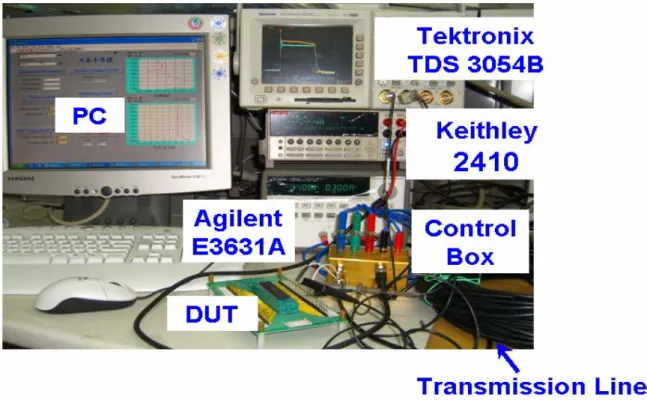
and integrated circuits in this thesis. The proposed LP-TLP system with two kinds of long pulse widths (500 ns/1000 ns) is evidently different from the traditional TLP system with a short pulse width of 100 ns. The LP-TLP system with a pulse width of 500 ns is consistent to the pulse width (~475 ns) of CDE in Fig. 2.6 (a). Thus, the LP-TLP system can be utilized to examine the damage situation on the DUT under CDE stress. Fig. 3.3 sketches the measurement setup for the proposed LP-TLP test. Besides, the actual measurement setup is shown in Fig 3.4. The measurement setup includes a diode, a load resistance (RL), a 50-m transmission line (or a 100-m
transmission line), two switches (SW1 and SW2), a high-voltage DC supply, a current probe, a voltage probe, and an oscilloscope.
The diode and the load resistance (RL) are defined as the polarization end to
absorb the reflection wave. The principle of LP-TLP operation is described as follows. In the initial state, the switch SW1 is short-circuit and the switch SW2 is open-circuit. Through high-voltage resistance RH, the high-voltage DC supply provides the
transmission line with a fixed voltage. The switch SW1 is open-circuit and the switch SW2 is short-circuit in the next state. The stored energy on the transmission line transfers to the DUT by the electromagnetic wave, and then the current and voltage pulses on the DUT are measured by the oscilloscope to obtain the first group data of the LP-TLP measured I-V curve. Afterward, the switch SW1 returns to short-circuit and the switch SW2 reverts to open-circuit. Through the high-voltage resistance RH,
the high-voltage DC supply provides the transmission line with a higher fixed voltage. The second group of current/voltage data is measured by repeating the aforementioned steps. The foregoing procedures are continuously duplicated until all I-V characteristics are measured. However, a permanent damage happens when the DUT is over-heated. With the aid of LP-TLP system, the secondary breakdown point of semiconductor devices under CDE stress can be measured.
3.2.2 Verification on LP-TLP with a Load of 50-Ω Resistor
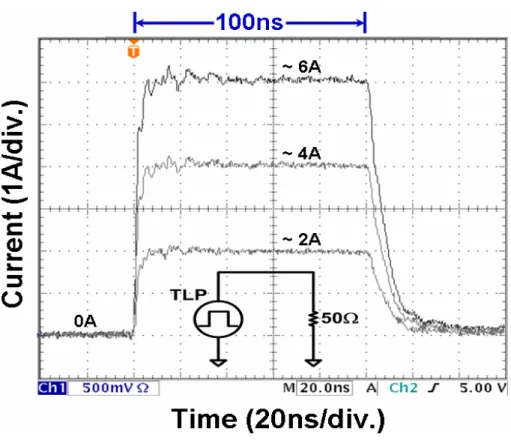
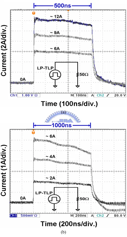
A 50-Ω resistor is used as the DUT to verify that the LP-TLP system can generate a long current pulse similar to cable discharge waveform. The LP-TLP measured current waveforms are shown in Figs. 3.5(a) and 3.5(b). When a 50-m transmission line is charged to 450 V, 640 V, and 880 V by the high-voltage DC supply, it will generates the corresponding LP-TLP currents of 6 A, 9 A, and 12 A into the 50-Ω resistor at DUT, respectively. So, the amplitude of current pulse is obviously increased while the charged voltage provided by the high-voltage DC supply is increased. Furthermore, the pulse width of these three current waveforms is 500 ns when the length of transmission line is 50 m, so the proposed LP-TLP system with a long current pulse width has been proven. If the length of long-pulse transmission line in the LP-TLP setup is 100 m, the generated current waveform has a pulse width of 1000ns, as shown in Fig. 3.5(b). Hence, it suggests that the LP-TLP pulse width is a function of the cable length of transmission line.
3.2.3 Verification on Gate-Grounded NMOS (GGNMOS)
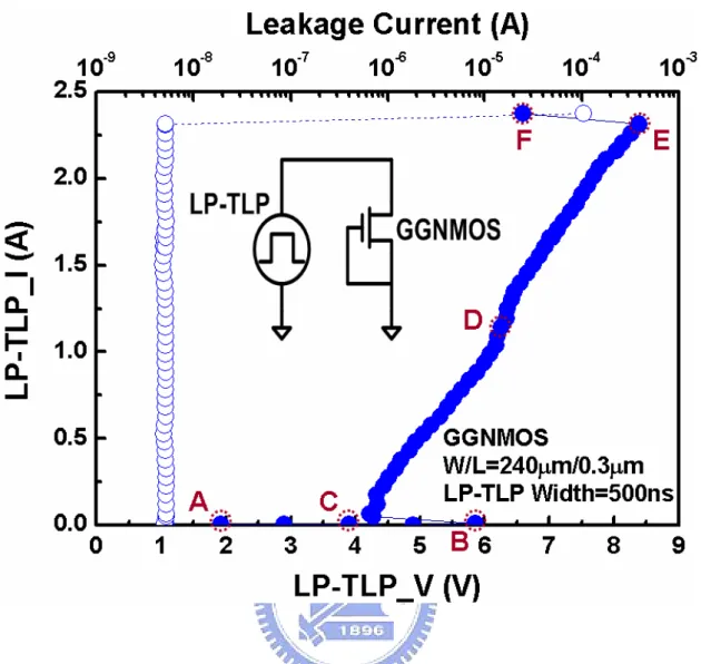
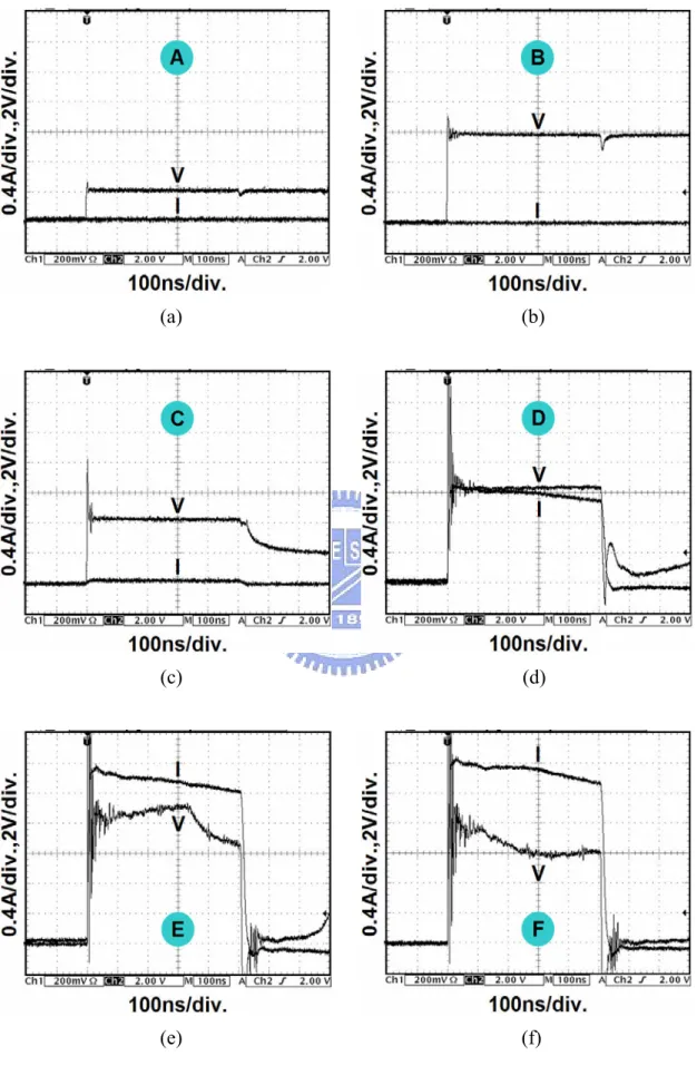
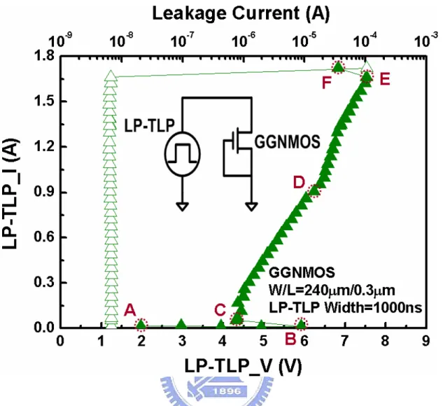
A gate-grounded NMOS (GGNMOS) device, which has been widely used as the on-chip ESD protection device in CMOS ICs, is regarded as the DUT to demonstrate that LP-TLP system can accurately measure its snapback characteristics and secondary breakdown current (It2). The 500-ns LP-TLP measured I-V characteristic of GGNMOS with a device dimension of W/L= 240 μm/0.3 μm is shown in Fig. 3.6. In addition, Figs. 3.7(a)-(f) exhibit the time-domain I-V waveforms of GGNMOS device at the corresponding points marked in Fig. 3.6. The I-V curves of GGNMOS device will shift from the initial point (A) to the trigger point (B) as the high-voltage DC supply continuously provides the higher energy. After passing through the trigger
point (B), the I-V curve will enter the snapback region because the parasitic lateral BJT in the GGNMOS device is turned on. The point C and the point D are the initial point and the middle point in snapback region, respectively. Subsequently, the curve will reach the critical point (E) called the secondary breakdown point of GGNMOS device. Furthermore, the corresponding current of secondary breakdown point is named the secondary breakdown current (It2). If the high-voltage DC supply further raises the charged voltage, the I-V curve will reach the point F into the secondary breakdown region, which causes the permanent damage on the GGNMOS device. Here, the failure criterion of silicon devices is defined when the leakage current of DUT exceeds 1 μA after the 500-ns LP-TLP stress. From the measured results, the 500-ns LP-TLP system can efficiently measure the snapback characteristics of GGNMOS device under CDE-like stress. Fig. 3.6 shows that the 500-ns LP-TLP measured trigger voltage is 5.9 V, the snapback voltage is 4.3 V, and the It2 is 2.3 A.
The 1000-ns LP-TLP measured I-V characteristic of GGNMOS with a device dimension of W/L= 240 μm/0.3 μm is shown in Fig. 3.8. Besides, Figs. 3.9(a)-(f) show the time-domain I-V waveforms of GGNMOS device at the corresponding points marked in Fig. 3.8. Similarly, the 1000-ns LP-TLP system can measure and analyze the secondary breakdown characteristic of GGNMOS device. Fig. 3.8 shows that the 1000-ns LP-TLP measured trigger voltage is 5.9 V, the snapback voltage is 4.3 V, and the It2 is 1.7 A. From the aforementioned tests, the 500-ns (1000-ns) LP-TLP system can be used to effectively observe the CDE robustness of DUT.
3.3 S
UMMARYA new proposed LP-TLP system with two kinds of long pulse widths (500 ns/1000 ns) is utilized to investigate the phenomenon of CDE event on IC products.
The snapback I-V characteristics and the secondary breakdown current (It2) of devices in CMOS ICs can be measured through the proposed LP-TLP system. Moreover, the proposed LP-TLP system can successfully observe the CDE robustness of DUT.
Fig. 3.1 The measurement setup for the traditional TLP test.
Fig. 3.2 The 100-ns TLP current waveforms on a 50-Ω resistor under different
Fig. 3.3 The measurement setup for the proposed LP-TLP test.
(a)
(b)
Fig. 3.5 The (a) 500-ns and (b) 1000-ns LP-TLP current waveforms on a 50-Ω
(a) (b) (c) (d) (e) (f)
Fig. 3.7 (a)-(f) The measured time-domain I-V waveforms of GGNMOS device at
(a) (b) (c) (d) (e) (f)
ig. 3.9 (a)-(f) The measured time-domain I-V waveforms of GGNMOS device at
the corresponding points marked in Fig. 3.8.
Chapter 4
Dependence of Layout Parameters on CDE
Robustness of CMOS Devices
4.1 NMOS/PMOS
IN A0.25-
μm
S
ALICIDEDCMOS
P
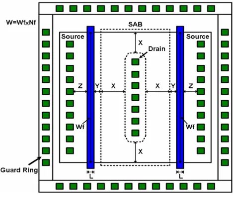
ROCESSIn order to design area-efficient CDE protection circuits, the CDE robustness of protection devices is considered as strong as possible in per unit layout area. To optimize the layout area, the layout spacings are the major considerations for designing strong CDE robustness devices. The main layout factors to affect the CDE level of CDE-protection devices are the channel width (W), the channel length (L), the finger width (Wf) of each finger, th spacing from source contact to poly-gate ote: the SAB layer is the silicide-blocking layer to block the silicided diffusion on the drain regions). Moreover, the descriptions for different layout parameters are shown in Table 4.1. When the dependence of CDE current paths on the layout parameters are well comprehended, CDE protection devices can be optimized to perform higher CDE robustness.
In this section, the dependence of these five layout factors on the CDE level of the gate-grounded NMOS (GGNMOS d gate-VDD PMOS (GDPMOS) are
understand the difference between the CDE level and the HBM ESD level, the long-pulse
the transmission line pulsing (TLP) used to measure the second breakdown characteristics of devices.
e
edge (Z), and the SAB width (X), which are illustrated in Fig. 4.1 (n
) an
practically investigated through fabricated silicon chips. To clearly
transmission line pulsing (LP-TLP) and techniques will be
The proposed LP-TLP and the conventional TLP measured data are compared the dependence on layout parameters as follows.
4
to find
.1.1 Channel Width
T leakage
urrents, and the turn-on resistances of GGNMOS devices with different channel widt
on resistances of GGNOS devices with different widths of 240 μm, 300 μm,
edge (Z), the distance from drain he 500-ns LP-TLP measured I-V characteristics, the corresponding
c
hs, but with the same channel length and unit-finger width, are shown in Fig. 4.2. From the measured results, all GGNMOS devices with different channel widths have distinct snapback characteristics. In addition, the It2 of the GGNMOS device is linearly increased with increasing the channel width. The It2 levels of GGNOS devices with different widths of 240 μm, 300 μm, 360 μm, and 600 μm under the proposed 500-ns LP-TLP test are 2.3 A, 2.9 A, 3.3 A, and 5.1 A, respectively. But, the turn-on resistance of GGNMOS device in snapback region is decreased with increasing the channel width. Here, the turn-on resistance is defined as the voltage variation over current variation before second breakdown in the 500-ns LP-TLP measured I-V curve. The turn-on resistance can be expressed as
Rdevice ≡ ∂VDS/∂ID (4.1)
The
turn-360 μm, and 600 μm under the proposed 500-ns LP-TLP test are2.05 Ω, 1.66 Ω, 1.36 Ω, and 0.87 Ω, respectively. The dependence of the It2 levels of GGNMOS and GDPMOS devices on the channel width under the traditional 100-ns TLP and the proposed 500-ns (1000-ns) LP-TLP tests is shown in Figs. 4.3(a) and 4.3(b), respectively. The unit-finger width (Wf) of GGNMOS and GDPMOS devices in the finger-type layout is kept at 30 μm. For both GGNMOS and GDPMOS devices, the channel length (L), SAB width (X), the clearance from SAB to poly-gate edge (Y), the spacing from source contact to poly-gate
diffusion to guard ring edge (G) are drawn as 0.3 μm, 3 μm, 0.3 μm, 0.75 μm, and Fig. 4.3(a), these It2 levels of GGNMOS devices are linearly incre
to the DUT device, which causes a w
2μm, respectively. In
ased while the channel width is increased. Besides, the It2 levels of GGNMOS devices under the traditional 100-ns TLP test are much higher than those under the proposed 500-ns (1000-ns) LP-TLP test. For instance, the It2 of GGNMOS device with a channel width of 360 μm under the traditional 100-ns stress is 5.3 A, but that with the same device dimension and layout style under the proposed 500-ns and 1000-ns LP-TLP tests are only 3.4 A and 2.4 A, respectively. Similarly, while the channel width is increased, the It2 levels of GDPMOS devices under the traditional 100-ns TLP and the proposed 500-ns (1000-ns) LP-TLP tests are all increased, as shown in Fig. 4.3(b). Furthermore, under the same device dimensions and layout style, the It2 levels of GDPMOS devices under 500-ns (1000-ns) LP-TLP stress are evidently lower than those under the traditional 100-ns TLP stress. Attributed to the longer LP-TLP pulse width, the stronger energy is injected in
eak robustness of the device under CDE stress.
4.1.2 Channel Length
The relations between the channel length and the It2 levels of GGNMOS and GDPMOS devices under the traditional 100-ns TLP and the proposed 500-ns (1000-ns) LP-TLP tests are illustrated in Figs. 4.4(a) and 4.4(b), respectively. The layout style and other parameters are all kept the same (W=360 μm, Wf=30 μm, X=3 μm, Y=0.3 μm, Z=0.75 μm, and G=2 μm), but only the channel length is different in this investigation. From the measured results in Fig. 4.4(a), when the GGNMOS device has a shorter enough channel length under the traditional 100-ns TLP test, the efficiency and performance of the parasitic lateral BJT in the GGNMOS device is significantly improved [16], [17]. Therefore, the GGNMOS device with a short
channel length (0.25 μm) can sustain much higher HBM ESD level than that with a medium channel length of ~0.35 μm. However, the GGNMOS device with a shorter channel length under the proposed 500-ns LP-TLP test has a lower It2, especially in a channel width of 0.25 μm. The It2 levels of GGNMOS devices under the proposed 1000-ns LP-TLP test are the lowest and not obviously varied with different channel lengths. Similarly, the It2 levels of GGNMOS devices under the traditional 100-ns TLP test are still higher than those under the 500-ns (1000-ns) LP-TLP test.
On the contrary, the GDPMOS device with a shorter channel length has a lower It2 under the traditional 100-ns TLP test and 500-ns (1000-ns) LP-TLP test, as shown in Fig. 4.4(b). Even if the GDPMOS device with a minimum channel length of 0.25 μm, their It2 levels under the traditional 100-ns TLP test and the 500-ns (1000-ns) LP-TLP tests are only 2.2 A, 1.18 A, and 0.95 A, because the turn-on efficiency of lateral p-n-p BJT in the GDPMOS device is not improved. From this experimental investigation, the selection of MOSFET for ESD and CDE protection is quite different
CMOS process. in the 0.25μm salicided
4.1.3 Unit-Finger Width
In the I/O cell layout of CMOS ICs, a large-dimension device is traditionally drawn with multiple fingers in a parallel connection. If the finger width (Wf) of every finger is shorter, more fingers must be used to form the same large-dimension device. The large-dimension device with different numbers of unit finger and unit-finger width can cause different ESD and CDE performances, even though the devices have the same channel width (W) and channel length (L) dimensions. The more multiple fingers of a large-dimension device are hard to be uniformly turned on during the ESD and CDE stresses, hence it may result in different ESD and CDE levels. To verify this issue, both the GGNMOS and GDPMOS devices with the fixed channel
width (W)/channel length (L) of 360 μm/0.3 μm but different unit-finger widths are investigated under the traditional 100-ns TLP and the 500-ns (1000-ns) LP-TLP tests. The tested results are shown in Fig. 4.5(a) and Fig. 4.5(b).
From the measured results, the It2 of GGNMOS devices of W=360 μm under the traditional 100-ns TLP stress is decreased from 5.61 A to 4.46 A as the GGNMOS devic
tness of GGNMOS and GDPMOS devices is much worse than their HBM ESD robustness under the same layout factor of the
e is drawn with the finger number from 8 to 24. When the GGNMOS device is drawn with the finger number from 24 to 8, the It2 levels of the GGNMOS devices of W=360 μm under the proposed 500-ns (1000-ns) LP-TLP stress are increased from 2.94 A to 3.39 A (2.22 A to 2.56 A). Similarly, the more finger number in the GDPMOS device leads to slightly lower ESD and CDE robustness. From the above-mentioned analysis, it implies that the finger-type GGNMOS and GDPMOS devices with a shorter finger width cannot be uniformly turned on during ESD and CDE stresses. Moreover, the CDE robus
unit-finger width.
4.1.4 Spacing from Source Contact to Poly-Gate Edge
The relationships between the spacing from the source contact to the poly-gate edge (Z) and the It2 levels of GGNMOS and GDPMOS devices under the traditional 100-ns TLP and the proposed 500-ns (1000-ns) LP-TLP tests are investigated in Fig. 4.6(a) and Fig. 4.6(b), respectively. In this investigation, all the layout style and other spacings are kept the same (W=360 μm, L=0.3 μm, Wf=30 μm, X=3 μm, Y=0.3 μm, and G=2 μm), but only the spacing Z is varied from 0.25 μm to 2 μm in the test chips. From the experimental results, the spacing Z varied from 0.25 μm to 2 μm only causes a slight variation on the It2 from 5.14 A to 5.25 A (2.12 A to 2.47 A) in the GGNMOS (GDPMOS) device under the traditional 100-ns TLP stress. Under the
proposed 500-ns LP-TLP stress, the It2 of GGNMOS (GDPMOS) is increased from 2.88
e of the It2 levels of GGNMOS and GDPMOS devices on SAB width (X) under the traditional 100-ns TLP and the proposed 500-ns (1000-ns)
ectively. The layout style and other
A to 3.34 A (1.13 A to 1.39 A) as the spacing Z is increased from 0.25 μm to 2 μm. However, the GGNMOS device with a shorter spacing Z under the proposed 500-ns LP-TLP stress has a lower It2 current, especially in the spacing of 0.25 μm. In addition, it also results in a little increase on the It2 from 2.3 A to 2.74 A (0.9 A to 1.16 A) of GGNMOS (GDPMOS) device under the proposed 1000-ns LP-TLP stress when the spacing Z varies from 0.25 μm to 2 μm. Only a little efficiency of the spacing Z can change the turn-on path of the parasitic lateral BJT owing to the source diffusions of MOSFET are connected with the bulk of MOSFET. Therefore, the spacing Z has no obvious impact on the ESD and CDE robustness of MOSFET.
4.1.5 SAB Width The dependenc
LP-TLP tests is shown in Figs. 4.7(a) and 4.7(b), resp
clearances are all kept the same (W=360 μm, L=0.3 μm, Wf=30 μm, Y=0.3 μm, Z=0.75 μm, and G=2 μm, but only the SAB width is different in this investigation. In Fig. 4.7(a), the It2 of GGNMOS device under the traditional TLP stress is increased as the SAB width is increased from 1.5 μm to 2 μm. Because the silicide blocking on the drain region introduces ballast resistance, it could limit ESD currents to flow through the channel surface of MOSFET. On the contrary, while the SAB width is increased from 2 μm to 5 μm, the It2 of GGNMOS device under the traditional 100-ns TLP test is decreased from 5.6 A to 4.1 A. Due to large increase of the SAB width (i.e. add too much silicide blocking), the power consumption along the ESD current path increases, resulting in a higher thermal stress and consequently a significantly lower It2. From the 100-ns TLP measured results, the maximum It2 of
GGNMOS device is with the SAB width of 2 μm. Under the proposed 500-ns (1000-ns) stress, the It2 trend of GGNMOS device is similar to the case under the traditional 100-ns TLP stress but with much lower current levels. However, the maximum It2 levels of GGNMOS device under the 500-ns (1000-ns) LP-TLP test are with the SAB width of 3 μm and 4 μm, respectively, as shown in Fig. 4.7(a).
On the contrary, in Fig. 4.7(b), the It2 levels of GDPMOS device under the traditional 100-ns TLP and the proposed 500-ns (1000-ns) LP-TLP stresses are all increased while the SAB width is increased from 0.75 μm to 5 μm. The phenomenon resulted from the existence of ballast resistance, which causes higher HBM ESD and From the experimental investigations, it is evident that the GGN
CDE robustness.
MOS and GDPMOS protection devices are very weak to withstand such CDE-induced high energy. Consequently, the It2 levels of CMOS devices under the 500-ns (1000-ns) LP-TLP stress are much lower than those under the traditional 100-ns TLP stress.
4.1.6 Failure Analysis
Figs. 4.8(a)-(c) reveal the scanning electron microscope (SEM) photographs of GGNMOS device (W/L=420 μm/0.3 μm) to observe the failure locations after the traditional 100-ns TLP test and the proposed 500-ns (1000-ns) LP-TLP test. As shown in Fig. 4.8(a), the failure locations are uniformly distributed among all fingers via the traditional 100-ns TLP test. Fig. 4.8(b) shows an obvious local failure region because the GGNMOS device is directly burned out from drain to common source in two fingers after the proposed 500-ns LP-TLP test. After the proposed 1000-ns LP-TLP test, not only a local damage site is seriously burned out from drain to source in one finger but also adjacent drain contact region is failed by a pinhole, as shown in Fig. 4.8(c). From these SEM pictures, the fingers in GGNMOS device cannot be
uniformly turned on during the proposed 500-ns (1000-ns) LP-TLP stress because of the CDE-induced higher pulse energy. This causes an evident reduction on the It2 of GGNMOS device under CDE events. By using the proposed 500-ns (1000-ns) LP-T
cess. Here, the other layout factors are the clearance from SAB to poly-gate edge (Y), and the distance from drain diffusion to guard ring edge (G). To ficiency of CMOS devices during CDE stress, the turn-on mech
LP test, one set of optimized design rules against CDE stress on chip layout in
IC products can be established in the given CMOS process.
4.2 NMOS/PMOS
IN A0.18-
μm
S
ALICIDEDCMOS
P
ROCESSIn this section, the dependence of other layout factors on the CDE capability of the GGNMOS and GDPMOS devices, which are different from the layout factors in section 4.1, are practically investigated through fabricated silicon chips in a 0.18-μm salicided CMOS pro
optimize the best turn-on ef
anisms of CMOS devices under high current stress must be understood and analyzed. By using the TLP and the LP-TLP systems, the optimal layout parameters can be found and investigated under ESD and CDE stresses.
4.2.1 Clearance from SAB to Poly-Gate Edge To investigate the I-V characteristics of the GGNMOS and GDPMOS devices with different Y parameters during ESD and CDE stresses, the TLP and LP-TLP measured I-V curves of the GGNMOS and GDPMOS devices with different Y parameters of –0.75 μm, -0.45 μm, -0.2 μm, -0.05 μm, 0.05 μm, 0.2 μm, and 0.45 μm are shown in Figs. 4.9(a) and 4.9(b). Here, the spilt conditions of –0.75 μm, -0.45 μm, -0.2 μm, -0.05 μm, 0.05 μm are meant that the silicide-blocking layer will overlap poly-gate edge 0.75μm, 0.45μm, 0.2μm, 0.05μm, respectively. In this investigation,
all of the layout style and other parameters are kept the same (W=360 μm, L=0.25 μm, Wf=30 μm, X=1.5 μm, Z=0.75 μm, and G=2 μm). In Fig. 4.9(a), the It2 of GGNMOS device under the 100-ns TLP test is increased from 3.1 A to 3.3 A when the Y parameter is increased from 0.05 μm to 0.45 μm. Similarly, the It2 of GGNMOS 2.6 A (1.9 to 2.1 A) as the clearance Y is varied from 0.05 μm to 0.45 μm. Because the larger Y pa
m to 0.05 μm only leads a slight variation on the It2 of GDPMOS device under the traditional 100-ns TLP
GDP
device under the 500-ns (1000-ns) LP-TLP test is improved from 2.3 A to A
rameter with larger spacing from drain contact to poly-gate edge can cause wider turn-on area in the parasitic lateral BJT of GGNMOS device under ESD and CDE stresses [16], the GGNMOS device can sustain the higher ESD and CDE robustness. In additional, the It2 of GGNMOS device under ESD and CDE stresses is all decreased while the overlap between the silicide-blocking layer and poly-gate is increased. In other words, if the silicide-blocking layer overlaps poly-gate too much, it will cause a significant degradation on the ESD and CDE reliability level of GGNMOS device.
On the other hand, the clearance Y varied from –0.075 μ to
test and the proposed 500-ns (1000-ns) LP-TLP test, as shown in Fig. 4.9(b). But, the MOS device with a larger clearance Y under ESD and CDE stresses has a lower It2, especially in a clearance Y of 0.2 μm.
4.2.2 Distance from drain diffusion to Guard Ring Edge
The distance from the diffusion to the substrate guard ring diffusion in the finger-type layout also has an evident impact on the CDE robustness of the GGNMOS device. The distance has been illustrated in Fig. 4.1 and marked as “G”. However, the longer distance G contributes a larger base resistance to the parasitic lateral n-p-n BJT in the GGNMOS device. The parasitic lateral BJT with a larger base resistance makes
itself to be triggered on more quickly and uniformly to bypass CDE current. The It2 of GGNMOS device with different G distances but the fixed other layout spacings (W=360 μm, L=0.25 μm, Wf=30 μm, X=1.5 μm, Y=0.45 μm, and Z=0.75 μm) is investigated in Fig 4.10. From the measured results, while the distance G is increased from 2 μm to 6 μm, the It2 of GGNMOS device under the traditional 100-ns TLP stress is improved from 3.29 A to 3.71 A. Besides, the It2 of GGNMOS device under the 500-ns (1000-ns) LP-TLP stress is also improved from 2.38 A to 2.78 A (1.95 A to 2.38 A) when the distance G is increased from 2 μm to 6 μm. This investigation confirms the important effect of the layout distance G on the ESD and CDE robustness. Because the larger distance from drain diffusion to guard ring edge (G) can enhance the turn-on uniformity of lateral BJT for all fingers in GGNMOS device, the GGNMOS device can sustain higher ESD and CDE currents.
ICs and rapid increase in operating frequencies, providing effective CDE protection to protect the internal circuits has a
of process development on CDE
4.3 C
OMPARISON BETWEEN0.25
μm
AND0.18
μm
CMOS
P
ROCESSESCDE event is one of the serious reliability issues in Ethernet IC manufacturing. With the continuous scaling of Ethernet
severe challenge. Therefore, in this section, the influence
capability is practically investigated through fabricated silicon chips in both 0.25-μm and 0.18-μm CMOS technologies. The relations between the channel width (channel length) and the It2 of GGNMOS device under the 500-ns LP-TLP stress in both 0.25-μm and 0.18-μm CMOS technologies are shown in Figs. 4.11(a) and 4.11(b), respectively. From the experimental results, due to the thinner gate oxide of GGNMOS in deep-submicron CMOS technologies, the CDE robustness of GGNMOS device with different channel widths (channel lengths) in 0.18-μm CMOS process is
much worse than those in 0.25-μm CMOS process. However, the maximum It2 of GGNMOS device in both 0.25-μm and 0.18-μm CMOS technologies is the same with the channel with of 600 μm, as shown in Fig. 4.11(a). But, the maximum It2 of GGNMOS device in 0.25-μm and 0.18-μm CMOS technologies is with the channel length of 0.3 μm and 0.5 μm, respectively, as shown in Fig. 4.11(b).
4.4 SCR
D
EVICE IN A0.18-
μm CMOS
P
ROCESSOwing to the low holding voltage (Vhold, about ~1.5 V in general CMOS process)
of silicon controlled rectifier (SCR) device [18], [19], the power dissipation (power = ×Vhold) located on the SCR device during CDE stress is significantly less than that
de evice. The SCR device can sustain a much higher CDE levels within a smaller layout area
ICDE
located on other CDE protection devices, such as the diode, BJT, MOS, or field-oxi d
in CMOS ICs, so it has been effectively used to protect the internal circuit against ESD and CDE damages. But, the SCR device still has a higher switching voltage (i.e., trigger voltage, ~18 V) in the deep-submicron CMOS technology, which is generally greater than the gate-oxide breakdown voltage of the input stages. Moreover, the gate-oxide thickness, the time-to-breakdown (tBD), or the
charge-to-breakdown (QBD) will also be decreased with shrinkage of CMOS
technology. Therefore, it is extremely important to reduce the switching voltage of SCR device and to enhance the turn-on speed of SCR device for successfully protecting the ultra-thin gate oxide from latent damage of the internal circuit [20].
In this section, the CDE robustness and the switching voltage of lateral SCR (LSCR) and modified lateral SCR (MLSCR) are practically investigated through fabricated silicon chips in a 0.18-μm salicided CMOS technology. Furthermore, the CDE and HBM ESD levels of SCR device are compared by means of the LP-TLP and
TLP techniques.
4.4.1 Lateral SCR (LSCR)
The lateral SCR (LSCR) device was used as an efficient input CDE protection e SCR is illustrated in Fig. .12, and the measured I-V characteristics of the SCR device under the 100-ns TLP and
S (GG
elem nt in CMOS ICs [18], [19]. The device structure of L 4
the 500-s (1000-ns) LP-TLP tests in a 0.18-μm CMOS process is shown in Fig. 4.13. In some applications, the N-well of LSCR device is connected to the input pad, but not to VDD, to eliminate the forward-bias diode from the pad to VDD. From the experimental results, the It2 of LSCR device with 61.62-μm width under the traditional 100-ns TLP stress is over 6A, but the It2 of LSCR device with 61.62-μm width under the 500-ns and 1000-ns LP-TLP stresses is reduced to be 4.5 A and 3.7 A, respectively. So, the CDE robustness of LSCR device is much worse than the ESD robustness of LSCR device. Under the 100-ns TLP and 500-ns (1000-ns) LP-TLP tests, the switching voltage and the holding voltage of LSCR device are about 18 V and 2.4 V, respectively. Hence, the LSCR device has the higher switching voltage (~18 V) in a 0.18-μm CMOS process, which is generally greater than the gate-oxide breakdown voltage of the input stages. To perform the overall CDE protection function to protect the input stages, the LSCR device needs the additional secondary protection circuit, such as the series resistor and the gate-grounded NMO
NMOS). The secondary protection circuit has to sustain CDE stress before the LSCR device is triggered on to discharge the CDE current on the input pad. Therefore, the design of the secondary protection circuit with the LSCR for the overall input CDE protection circuit is somewhat critical in the CMOS ICs.
4.4.2 Modified Lateral SCR (MLSCR)
ign or layout on the secondary protection circuit still causes the CDE damage located on the secondary
SCR structure I. Consequently, an excellent desig
In order to reduce the switching voltage of LSCR device to provide more effective CDE protection for the internal circuits, the modified lateral SCR (MLSCR) device was invented [21]. The device structure I of MLSCR is illustrated in Fig. 4.14, and the measured I-V characteristics of MLSCR structure I under the 100-ns TLP and the 500-ns (1000-ns) tests in a 0.18-μm CMOS process is shown in Fig. 4.15. The MLSCR structure I is formed by inserting an additional N+ diffusion across N-well/P-substrate junction to lower the avalanche breakdown voltage of N-well/P-substrate junction. From the measured results, the It2 of MLSCR structure I with 61.62-μm width under the traditional 100-ns TLP and the 500-ns LP-TLP stresses is all over 6 A, but the It2 of MLSCR structure I with 61.62-μm width under the 1000-ns LP-TLP stress is reduced to be 5.4 A. Thus, under the same device dimension, the CDE robustness of MLSCR structure I is much better than that of LSCR device. The switching voltage and the holding voltage of MLSCR structure I under the traditional 100-ns TLP and the 500-ns (1000-ns) LP-TLP tests are about 11 V and 1.6 V, respectively. However, the switching voltage (~11 V) of MLSCR structure I is still larger than the gate-oxide breakdown voltage of input stages in the same process. Therefore, the MLSCR structure I has to be still cooperated with the secondary protection circuit to perform the overall CDE protection function to the input stages. Due to the lower switching voltage (~11V) of MLSCR structure I in the 0.18-μm CMOS technology, the secondary protection circuit could have smaller device dimensions to save total layout area. Improper des
protection circuit rather than the ML
n or layout of the secondary protection circuit with MLSCR structure I for the whole input CDE protection circuit is imperative in the Ethernet ICs.
Another device structure II of MLSCR is illustrated in Fig. 4.16, and the measured I-V characteristics of MLSCR structure II under the traditional 100-ns TLP and the 500-ns (1000-ns) LP-TLP stresses in a 0.18-μm CMOS process is displayed in Fig. 4.17. The MLSCR structure II is made by inserting an additional P+ diffusion across the N-well/P-substrate junction to lower the avalanche breakdown voltage of N-well/P-well junction. In Fig. 4.18, the It2 of MLSCR structure II with 61.62-μm width under the traditional 100-ns TLP and the 500-ns LP-TLP stresses is all over 6 A, but the It2 of MLSCR structure II with 61.62-μm width under the 1000-ns LP-TLP stresses is diminished to be 5.2 A. In addition, the switching voltage and the holding voltage of MLSCR structure II under the traditional 100-ns TLP and the 500-ns (1000-ns) LP-TLP tests are about 12 V and 1.8 V, respectively. Thus, under the same device dimension, the HBM ESD robustness, the CDE robustness, the switching voltage, and the holding voltage of MLSCR structure II are similar to those of MLSCR structure II. Because the switching voltage (~12 V) of MLSCR structure II is still greater than the gate-oxide breakdown voltage of input stages in the same process, the MLSCR structure II also needs the extra secondary protection circuit to perform the overall CDE protection function to protect the input stages.
4.5 A
PPLICATION OFLP-TLP
S
YSTEMNetwork equipment engineers are demanded to continually improve system-level performance while sustaining a high reliability of Ethernet IC products and robust environmental performance. In particular, the device or product failure rates of Ethernet local area network (LAN) industry were attributed to a “Cable Discharge Event” (CDE) phenomenon. Therefore, CDE event is an increasingly significant reliability concern that requires recognition at all levels in the networking industry.
Multiple CDE events could also occur when cable with some charges is plugged in and pulled out many times on Ethernet integrated circuits. This event can lead the cable modems, the Ethernet interfaces and the video equipments to be damaged. Therefore, this issue can be experimentally investigated in more detail by applying the long-pulse transmission line pulsing (LP-TLP) with fixed low zapping energy but multiple zapping times.
The measured I-V curves and the corresponding leakage currents of GGNMOS devices with W/L= 240 μm/0.25 μm fabricated in 0.18-μm CMOS process under the 500-ns LP-TLP stress and the 100-ns TLP stress are shown in Fig. 4.18. From the measured results, the trigger voltage, the snapback voltage, and the turn-on resistance in snapback breakdown region are nearly equivalent under the 500-ns LP-TLP and 100-ns TLP stresses except for the secondary breakdown current (It2). Besides, the It2 (1.19 A) under the 500-ns LP-TLP stress is much lower than the It2 (2.35 A) under the 100-ns TLP stress. The results suggested that the longer LP-TLP current pulse width will lead a stronger energy to inject into the GGNMOS device, which causes a weak
like stress.
order to simulate the influence of CDE event, which could be caused by cable plug
robustness of the GGNMOS device under CDE-In
ging in and pulling out many times on Ethernet integrated circuits, the 500-ns LP-TLP system of repeatedly zapping with fixed energy is used as an efficient measurement method to investigate this issue.
Fig. 4.19 illustrates the profile for energy of zaps versus number of zaps to failure relationship under the 500-ns LP-TLP and 100-ns TLP stresses. Energy of zaps (%) is defined as how larger CDE energy per zap will stress DUT. For example, the 90% energy of zaps means that the 50-m transmission line in LP-TLP setup is charged to a fixed voltage (90%×Vcharged) by high-voltage DC supply, then it will generate the corresponding LP-TLP current (90%×It2) stress into the GGNMOS device at DUT.
Here, Vcharged is defined as the charged voltage provided by the high-voltage DC-supply when the 500-ns LP-TLP I-V curve in Fig. 4.18 reaches the secondary breakdown current (It2=1.19 A). A GGNMOS device is “failed" if its leakage curre
240 μm/0.25 μm) with appli
and source are connected together to GND
nt exceeds 1μA. From the measured results, it clearly indicates that the number of zaps to failure is increased while the energy of zaps is decreased.
The profile for leakage current versus number of zaps to failure under LP-TLP current (90%×It2) stress (repeatedly zapping of fixed 90% energy) is shown in Fig. 4.20. The leakage current of GGNMOS device with W/L=240 μm/0.25 μm keeps at ~ nA order before the number of zaps is 892. However, the leakage current of GGNMOS device abruptly rises to ~100 μA when the number of zaps is 893. The experimental result reveals that the leakage current of GGNMOS device is not gradually increased while number of zaps is increased.
The measured DC I-V curves of GGNMOS device (W/L=
ed voltage at drain node and source node under different stress conditions are shown in Figs. 4.21(a) and 4.21(b), respectively. The DC I-V characteristic of GGNMOS device is measured by the HP4156B semiconductor parameter analyzer. If the DC voltage is applied at drain node, gate
, as shown in Fig. 4.21(a). On the contrary, if the DC voltage is applied at source node, gate and source are connected together, whereas drain is connected to GND, as shown in Fig. 4.21(b).
In Fig. 4.21(a), the measured current level in fresh condition is similar to that after number of zaps=888. After number of zaps=893 to failure under LP-TLP current (90%×It2) stress (repeatedly zapping of fixed 90% energy), the GGNMOS device was annealed at 125ºC for 20 hours and the DC I-V measurement was repeated. However, the current level of GGNMOS device is not significantly reduced and a very large amount of reverse leakage current of GGNMOS device is still the same as failure
(after number of zaps=893). So, the semiconductor device would be permanently damaged by repeatedly zapping of fixed low energy. Similarly, Fig. 4.21(b) also displ
m drain to source in one finger. Simi
f layout spacings on the CDE robustness of CMOS device in salic
ays the situation which is described above.
Figs. 4.22(a) and 4.22(b) exhibit the scanning electron microscope (SEM) pictures of GGNMOS device to observe the failure conditions after 500-ns LP-TLP stress with continuously zapping with increasing energy to fail and repeatedly zapping with fixed 90% energy to fail. After 500-ns LP-TLP stress of continuously zapping with increasing energy to fail, Fig. 4.22(a) shows an obvious local failure region because the GGNMOS device is directly burned out fro
larly, in Fig. 4.22(b), there is still an evident local failure site because of punching through from drain to source in one finger. So, from the failure analysis, the GGNMOS device can be damaged after many times of 500-ns LP-TLP stresses by repeatedly zapping with fixed energy.
4.6 S
UMMARYThe dependence o
ided CMOS process has been investigated and discussed in detail. Generally, the device with a wider channel width, a longer channel length, a wider unit finger width, a larger SAB width, a wider spacing from source contact to poly-gate edge, a larger clearance from SAB to poly-gate edge, and a far distance from drain diffusion to guard ring edge leads to a higher CDE robustness. From the measured results, the It2 levels of GGNMOS and GDPMOS devices under the proposed 500-ns (1000-ns) LP-TLP test are much lower than those under the traditional 100-ns TLP test. Therefore, CDE event has been confirmed to cause a significant degradation on the reliability of ESD-protected IC products.
Table 4.1
The descriptions for different layout parameters.
Parameter Description W Channel width
L Channel length Wf Unit-finger width
X Silicide-blocking (SAB) width Y Clearance from SAB to poly-gate edge
Z Spacing from source contact to poly-gate edge G Distance from drain diffusion to guard ring edge
![Fig. 2.2 The CDE voltage levels of Ethernet transceivers under different IC designs and process technologies [3], [4]](https://thumb-ap.123doks.com/thumbv2/9libinfo/8749207.205530/23.892.146.745.564.1022/voltage-levels-ethernet-transceivers-different-designs-process-technologies.webp)
![Fig. 2.6 Cable discharge waveforms when (a) unused pairs connected together and grounded and (b) unused pairs floating [5]](https://thumb-ap.123doks.com/thumbv2/9libinfo/8749207.205530/26.892.139.752.102.1054/cable-discharge-waveforms-unused-connected-grounded-unused-floating.webp)