國 立 交 通 大 學
光電工程研究所
博
士
論
文
非極性氮化鎵光電元件之磊晶成長
Epitaxial growth of nonpolar GaN based
optoelectronic devices
中 華 民 國 九 十 八 年 六 月
研 究 生: 柯宗憲
Student: Tsung-Shine Ko
指導教授:
郭浩中 教授
盧廷昌 教授
Advisor:
Dr. Hao-Chung Kuo
Dr. Tien-Chang Lu
非極性氮化鎵光電元件之磊晶成長
Epitaxial growth of nonpolar GaN based
optoelectronic devices
研 究 生:柯宗憲 Student:Tsung-Shine Ko
指導教授:郭浩中教授 Advisor: Dr. Hao-Chung Kuo
盧廷昌教授
Dr. Tien-Chang Lu
國 立 交 通 大 學 電機資訊學院
光電工程研究所
博 士 論 文
A dissertation
Submitted to Institute of Electro-Optical Engineering
College of Electrical Engineering and Computer Science
National Chiao Tung University
in partial Fulfillment of the Requirements
for the Degree of
Doctor of Philosophy
in
Department of Photonics & Electro-Optical Engineering
June 2009
Hsinchu, Taiwan, Republic of China
非極性氮化鎵光電元件之磊晶成長
研究生:柯宗憲
指導教授:郭浩中教授
盧廷昌教授
國立交通大學光電工程研究所
摘要
本論文旨在探討以有機金屬氣相沈積系統來成長非極性a面氮化鎵為主之光電材 料與元件,包含了優化成長、減少材料缺陷、主動層氮化銦鎵量子井結構設計,最後 完成a平面氮化鎵發光二極體製作與元件特性分析。 在磊晶之優化成長方面,我們利用有機金屬氣相沉積系統於高溫低壓下的成長環 境下獲得高品質非極性a平面氮化鎵薄膜,改變成核層氮化鋁厚度與成長氮化鎵時的 五三比,亦會影響非極性氮化鎵薄膜之品質。對於非極性氮化鎵之成長機制,我們利 用Wulff圖形的概念以及選區成長的方法來分析非極性氮化鎵成長於r面藍寶石基板上 的成長行為,此方法可以解釋非極性表面條紋以及坑洞的成因,並可進而預測成長, 提供非極性氮化鎵成長之準則。 由於非極性a 面氮化鎵成長不易,並具有很高的缺陷密度,因此在本論文中我們 提出溝槽式磊晶側向成長以及氮化銦鎵/氮化鎵超晶格層的運用,來改善材料品質, 由穿遂電子顯微鏡顯的結果,溝槽式磊晶側向成長可使a 平面氮化鎵薄膜於氮極性方 向上之晶格品質有明顯的提升,差排密度由原先的 1×1010 cm−2 減少至 3×107 cm−2,而在氮化銦鎵/氮化鎵超晶格層的部份,差排密度可有效地從 3×1010 cm-2降低 到9×109 cm-2。此部份實驗確認達成晶格品質提升之目的與商業化的可行性。 為優化後續的非極性藍光雷射二極體的元件結構,我們改變非極性氮化銦鎵量子 井的厚度並分析其光學特性。時間解析光致激發光譜結果指出當厚度逐漸變厚時,量 子井產生的激子生命期逐漸增加。而在變溫的光致激發光譜中,我們發現在量子井厚 度較薄的樣品具有較大的侷域深度可以有效地補獲激子,而較厚的樣品由於受到成長溫度較長時間下的影響使得其侷域紊亂程度變得更為嚴重導致發光效率明顯下降。 在製作發光二極體方面,我們運用溝槽式磊晶側向成長之a 面氮化鎵作為基板, 成功地在上面成長了發光二極體結構,發現該結構由於具有兩種不同缺陷密度之區 域,因此在改變電流下,發光波長會因為電流流經不同區域而有所不同,在注入電流 為140 mA 時功率為 0.2 mW;另外,在氮化銦鎵與氮化鎵組成的超晶格層部份,電 致激發光譜的結果證實此樣品在強度上亦有3.42 倍的增強,此元件並具有 56.3%的 偏振率。 因此,於本論文中我們已完成了非極性氮化鎵材料的成長以及元件製作相關的研 究,成果包含了成長條件優化、成長行為以及量子井結構與光學分析,另外,我們亦 提出數種可改善材料品質的方法,將在本論文中逐一討論並證明其可行性。我們冀望 這一系列的實驗對未來在非極性氮化鎵之光電元件發展而言,提供有用的資訊與助 益。
Epitaxial growth of nonpolar GaN based
optoelectronic devices
Student : Tsung-Shine Ko
Advisor : Dr. Hao-Chung Kuo
Dr. Tien-Chang Lu
Department of Photonics & Institute of Electro-Optical Engineering National Chiao Tung University
Abstract
In this dissertation, the epitaxial growth of nonpolar a-plane GaN based optoelectronic materials grown using metal organic chemical vapor deposition (MOCVD) have been investigated. Main works include optimum growth, InGaN multiple quantum wells (MQWs) design, reduction of defects and the fabrication of a-plane GaN based optoelectronic devices and analysis of device characteristics.
For optimum growth of a-plane GaN, we confirmed variation of thickness of AlN nucleation layer and V/III ratio of a-plane GaN growth influence crystal quality of a-plane GaN thin film. We also tried to figure out the mechanism of a-plane GaN by using Wulff plot and selective area growth to analyze the growth behavior of a-plane GaN grown on r-plane sapphire, which could be useful to explain the reasons account for stripes and pits exist on a-plane GaN surface and give us a guidance to predict growth of a-plane GaN.
In this dissertation, we used trench epitaxial lateral over growth (TELOG) and InGaN/GaN supperlattices (SLs) to improve crystal quality of a-plane GaN. The threading dislocation (TD) density can be reduced largely from 1×1010 cm−2 to 3×107 cm−2 for the N-face GaN wing. As for SLs part, The TD density in the sample with SLs was reduced from 3×1010 cm-2 down to ~9×109 cm-2.
For active layer structural design, a-plane InGaN/GaN MQWs of different width ranging from 3 nm to 12 nm have been grown. The peak emission intensity of the photoluminescence (PL) reveals a decreasing trend as the well width increases from 3 nm to 12 nm. Low temperature (9 K) time-resolved PL (TRPL) study shows that the sample with 3 nm-thick wells has the best optical property with a fastest exciton decay time of 0.57 ns. More effective capturing of excitons due to larger localization energy Eloc and shorter radiative lifetime of localized excitons are observed in thinner well width samples were observed in the temperature dependent PL and TRPL.
In development of nonpolar light-emitting diodes (LEDs), we successfully fabricated a-plane LEDs structure by using TELOG GaN substrate. Due to there are two areas with different defect density in this kind sample, the emission wavelength will be changed when we increased injection current. The power was 0.2 mW at 140 mA injection current. On the other hand, we also fabricated nonpolar LEDs by using InGaN/GaN SLs layer. Electroluminescence intensity of the sample with InGaN/GaN SLs was enhanced by a factor of 3.42 times to that of the conventional sample without InGaN/GaN SLs.
In this dissertation, we have achieved the studies on the growth of a-plane GaN and the fabrication of devices. Whole achievements include optimum growth, MQWs structural design, crystal improvement of material and fabrication of a-plane LEDs. We hope this series of experiments to provide a useful information and support for development of nonpolar optoelectronic devices in future.
Acknowledge 完成這本博士論文的工作,並非我一人所能獨立完成,回首過去五年來的博士班 生涯,除了自己的學習與充實,我更要感謝一路陪我走來的師長、朋友們,畢竟沒有 這些人的扶持,我不可能完成這本論文、不可能得到這個學位、亦不可能蛻變為現在 具觀察力、創新力、以及獨立思考能力的我。 首先我必須感謝我的指導老師們:王興宗教授、郭浩中教授以及盧廷昌教授,在 王老師對學術知識追求的渴望、郭老師對研究結果的務實、以及盧老師對實驗過程的 嚴謹風格帶領之下,著實讓我在博士班前四年,立下良好的學習基礎,更能展現個人 的研究特色。另外,我亦十分感謝美國耶魯大學韓仲教授,千里馬的這一年時間,在 他優秀學者風範的耳濡目染與薰陶之下,讓我的研究能力得到另一個提升,並敞開我 對學術的視野。 我非常感謝德忠在磊晶知識上無私地傳授與經驗上的分享,讓我得以迅速地在這 領域進入狀況,說真的,我欠你好幾頓的!家璞你不止在材料分析上的實驗大力幫忙 外,在英文上更是一起互相砥礪、學習的好伙伴,我會努力幫你找對象的。也感謝潤 琪在量測上的全力輔助與建設性的討論,雖然妳已經死會了,但我仍然積極地幫妳物 色好伴侶。家銘亦是幫忙執行任務的好伙伴,希望你在台大的日子,可以過得充實又 愉快。立夫你是我帶過最為憨直的一位學弟,感謝你在我最後兩年的日子,給予我的 幫助,一切盡在不言中!俊榮的獨特性與學者氣息,令我深深的著迷,可惜我不是女 的!李博、碩均、輝閔,不好意思,我得先走一步了,以後還會遇見你們,和你們在 一起的日子,真的很快樂。此外,亦感謝謝文峰老師實驗室的阿政學長、同慶學長、 維仁學長、楊松等人在實驗上的幫忙,你們的專業能力、樸實善良,都值得我們效仿。 而其它沒有列出的實驗室成員,別以為你們不重要,我真的也很感謝您們,只是礙於 篇幅,我只好忍痛將你們留在我心中了! 最後,我感謝我母親支身一人在家鄕的等待!我畢業了!可以回去照顧妳了!我 亦感謝我的家人、親戚,所給我的鼓勵與支持!最可愛的小秋美,感謝妳這段日子不 離不棄地和我在一起,有妳的扶持,讓我生命變得更為燦爛!謝謝你們!
Contents
Abstract (in Chinese) I
Abstract (in English) III
Acknowledge V
Contents VI
List of figures IX
List of tables XIV
Chapter 1 Introduction
11-1 Historical review of nitride based LEDs 1
1-1-1 Wurtzite III-nitride material property 1
1-1-2 Milestones for nitride based LEDs 3
1-1-3 Spontaneous and piezoelectric polarizations 6
1-2 Historical review of nonpolar GaN growth 8
1-2-1 Material characteristics of nonpolar GaN 8
1-2-2 Growth of nonpolar GaN 11
1-2-3 Nonpolar GaN applications 17
1-3 Challenges to grow nonpolar GaN based LEDs 21
1-3-1 Morphology 21
1-3-2 Threading dislocations & Stacking faults 22
1-4 Motivation 24
References 26
Chapter 2 Experimental instruments and physical models
30 2-1 Metal organic chemical vapor deposition, MOCVD 302-1-1 MOCVD equipment 30
2-1-2 MOCVD precursors 34
2-1-3 III-Nitride MOCVD growth 35
2-2 Electron microscopes 37
2-2-1 Basic principle of electron microscope 37
2-2-2 Scanning electron microscope 38
2-2-3 Transmission electron microscope 39
2-2-4 Cathodoluminescence 41
2-3 Atomic force microscope 42
2-3-1 Advantages of atomic force microscope 42
2-3-2 Scan modes of atomic force microscope 43
2-4 X-ray diffraction 44
2-4-2 X-ray diffraction system 46 2-5 Photoluminescence, PL 46 2-5-1 Temperature dependent PL 47 2-5-2 µ-PL 49 2-5-3 Time-resolved PL systems 50 2-6 Electroluminescence, EL 52 2-7 Furnace 53 References 55
Chapter 3 Development and optimization of a-plane GaN
growth on r-plane sapphire
563-1 Difficulties to grown nonpolar GaN 56
3-2 Experimental procedure 57
3-3 Effects of different growth temperatures and pressures 58
3-4 Roles of V/ III ratio and nucleation layer 61
3-5 Observation of threading dislocation in nonpolar GaN 64
3-6 Summary 65
References 67
Chapter 4 Understanding nonpolar GaN growth
694-1 Wulff-plot and motivation 69
4-2 Experimental procedure 70
4-3 Forming facet of nonpolar GaN island 72
4-4 Wulff-plot of nonpolar GaN under different growth conditions 74
4-5 Reasons for pit generation in nonpolar GaN 77
4-6 Summary 80
References 81
Chapter 5 Improvement of crystal quality in nonpolar GaN
845-1 Methods to reduce defects of nonpolar GaN 84
5-2 Experimental procedure 85
5-2-1 Trench epitaxial lateral overgrowth technique (TELOG) 85
5-2-2 The use of InGaN/GaN superlattices 86
5-3 Growth behavior of nonpolar GaN using TELOG 87
5-4 Defects reduction of using InGaN/GaN superlattices 89
5-5 Summary 91
References 93
Chapter 6 Optical properties of nonpolar InGaN/GaN multiple
quantum wells
946-1 Motivation 94
6-2 Sample preparation and optical measurements 95
6-3 PL characteristics of a-plane InGaN/GaN MQWs 97
6-4 Localization features in a-plane InGaN/GaN MQWs 101
6-5 Analysis of localization depth 105
6-6 Three-level localized exciton model 108
6-7 Summary 111
References 112
Chapter 7 Nonpolar optoelectronic devices
1157-1 Motivation 115
7-2 Sample process and experiments 116
7-3 Effect of TELOG structure on electronic properties 119
7-4 Performance of nonpolar TELOG LEDs 120
7-5 Performance of nonpolar blue LEDs using superlattices 123
7-6 Summary 125
References 127
Chapter 8 Conclusion and future work
129List of figures
Chapter 1
Fig. 1-1 Unit cell of wurtzite GaN crystal………2 Fig. 1-2 The band gaps of nitrides vs. their lattice constant a………3 Fig. 1-3 Band edges of conduction and valence bands………..7 Fig. 1-4 The monolayer schematic of atomic distribution in c-plane GaN
and a-plane GaN………...9 Fig. 1-5 PL spectra of m-plane GaN under different polarized angle
measurements……….10 Fig. 1-6 Left image is the structural characterizations of hexagonal GaN
grown on r-LiAlO2………11 Fig. 1-7 TEM and AFM images of a-plane GaN grown on sapphire………12 Fig. 1-8 Left is the schematic of radiative emission of m-plane GaN/AlGaN MQWs and PL spectra; Right is the AFM image which shows the surface morphology of m-plane GaN………...12 Fig. 1-9 a-plane GaN stripes along different directions using LEO………..13 Fig. 1-10 AFM images of surface morphology of a-plane GaN grown on (a)
nanorods structure and (b) regular GaN………13 Fig. 1-11 SEM cross section image of a-plane GaN grown using SALE
technique………14 Fig. 1-12 Left image investigated crystal quality of a-plane GaN grown
using different techniques examined by XRD analysis…………14 Fig. 1-13 Triangle defect type in a-plane GaN………15 Fig. 1-14 TEM images of a-plane GaN grown by HVPE………16 Fig. 1-15 The structural design in left figure and the results using r-plane
sapphire with different off-cut angles……….16 Fig. 1-16 AFM images of a-plane GaN surface (a) without (b) with SiNx
nanomask………...17 Fig. 1-17 Left schematic is the structure of first a-plane LED; right figure
shows the luminescence spectra with different injection currents. ……….18 Fig. 1-18 Left figure is the designed structure of a-plane blue LED using
ELOG technique. Right figure is the spectrum results with different currents………18 Fig. 1-19 Left figure shows the typical structure of LED grown on free
standing substrate; right figure is the output power of this device as a function of drive current………19
Fig. 1-20 Schematic of the LDs with the stripe parallel to c-axis in left figure;
L-I characteristics of c- and a-axis stripe LDs in right figure…...20
Fig. 1-21 The number of publications peryear focused on nitrides with polar, nonpolar and semipolar surfaces versus time…………...21
Fig. 1-22 Bright field TEM images of a plan-view sample parallel lines represent stacking faults formed on the basal plane of GaN….23
Chapter 2
Fig. 2-1 (a) Horizontal reactor and (b) vertical reactor in MOCVD system.32 Fig. 2-2 Source bubbling and mass flow controller schematic……….33Fig. 2-3 In-situ reflectance measurement during MOCVD growth………...36
Fig. 2-4 The schematic of SEM equipment……….39
Fig. 2-5 The schematic of TEM equipment……….40
Fig. 2-6 Schematic diagram showing the operating principles of the AFM in the contact mode……….43
Fig. 2-7 Schematic of X-ray measurement system………45
Fig. 2-8 Radiative recombination transitions in semiconductor materials. ……….47
Fig. 2-9 Schematic of temperature-dependent PL setup………48
Fig. 2-10 Schematic of µ - PL system………..50
Fig. 2-11 Schematic of TRPL system………...51
Fig. 2-12 EL system includes all components……….52
Fig. 2-13 Two-zone furnace picture and schematic figure………54
Chapter 3
Fig. 3-1 OM images of a-plane GaN surfaces for growth temperatures of 1020~1120 oC and pressures of 100~300 torr………58Fig. 3-2 Surface profiles of a-plane GaN epi-layers for growth temperatures of 1020~1120 oC and pressures of 100~300 torr. X is the scan direction along [1100], and Z is the height direction along [1120]. ………59
Fig. 3-3 SEM images of a-plane GaN surfaces for growth temperatures of 1020~1120 oC and pressures of 100~300 torr………...60
Fig. 3-4 AFM images of a-plane GaN surfaces for growth of V/III ratio of 600~1200 and on different thickness of nucleation layer………..63
Fig. 3-5 Reciprocal space mapping of a-plane GaN for growth temperatures of 1020~1120 oC and pressures of 100~300 torr..64 Fig. 3-6 Bright field (a) and dark field (b) cross-section TEM images of GaN
epilayer grown under optimal condition with g vector [1120]…...65
Chapter 4
Fig. 4-1 [(a) and (c)] SEM top views and [(b) and (d)] perspective views (60o inclined from a-axis to the in-plane m-axis) of the same a-GaN SAG mesa [(a) and (b)] before and [(c) and (d)] after a 10-min regrowth under condition A. The 5 µm scale bar applies to all the figures………...71 Fig. 4-2 Kinetic Wulff plots of prism planes mapped onto the basal plane for
growth conditions (a) A, (b) B, and (c) C. The region below the horizontal axis corresponds to the SiO2 mask………73 Fig. 4-3 Kinetic Wulff plots of the orientations mapped onto a-planes for
growth conditions (a) A, (b) B, and (c) C. The inner red trace represents the facets that are in contact with the mask and the outer blue trace the equivalent facets that are 60º rotated around c-axis (the two sets of facets are marked by blue and red lines in Fig. 4-1(b)). The traces below the horizontal axes, especially the position of the {1011} cusps, are hypothetical………74 Fig. 4-4 In situ optical reflectance of a-GaN growth on r-Al2O3 with a
HT-AlN buffer. The growths of a-AlN buffer and a-GaN are
marked out by shaded blue area………..76 Fig. 4-5 SEM (a) top view of m-GaN SAG mesas coalescing along c-axis;
(b) perspective view of m-GaN nucleation islands on AlN/m-SiC. The coalescence between inclined {1011} and vertical (0001) (marked by red dash lines) greatly contributes to the striation along a-axis………..77 Fig. 4-6 SEM (a) top view and (b) perspective view (60o inclined from
a-axis to [0001]) of the same a-GaN SAG mesa; (c) SEM top view of planar a-GaN/r-Al2O3 surface with many pits resembling the concave void in the SAG mesa, marked out by the red dot lines. ………..79 Fig. 4-7 SEM perspective views of (a) a-GaN and (b) m-GaN SAG concave
mesas grown out of the same annular openings in one OMVPE run under condition C. The both images are 60o inclined from the growth axis to the in-plane nonpolar axis………80
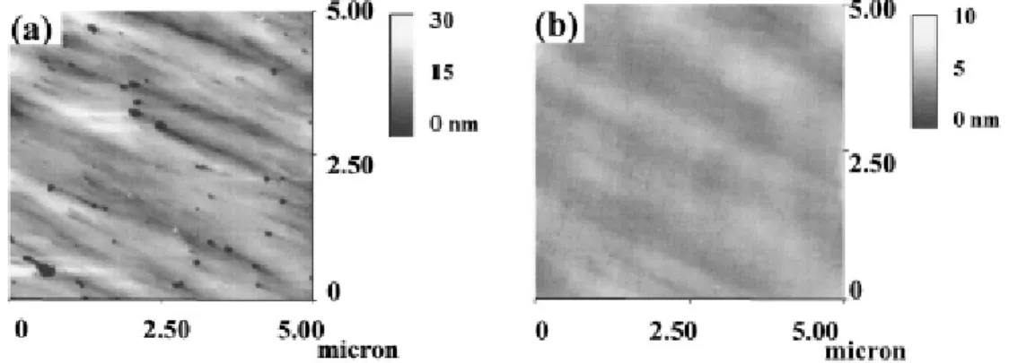
Chapter 5
Fig. 5-2 Cross-sectional SEM of the un-coalesced TELOG a-plane GaN film with 2 µm seed /18 µm trench pattern……….87 Fig. 5-3 Cross-sectional TEM g=(0002) and g=(1120) two beam bright field
images………...………….88 Fig. 5-4 Cross-sectional SEM of fully coalesced TELOG a-plane GaN film
with 2 µm seed /18 µm trench pattern………89 Fig. 5-5 Cross sectional TEM image of a-plane GaN with SLs.…………...90 Fig. 5-6 Arrhenius plots of the normalized integrated PL intensity over the
temperature range 90–300 K for (a) Sample.1 and (b) sample.2 ………...………..91
Chapter 6
Fig. 6-1 (a) Room temperature PL spectra of a-plane InGaN/GaN MQWs with well width ranging from 3~12 nm. (b)Normalized PL intensity and energy peak plotted as a function of quantum well width…98 Fig. 6-2 The relation between PL intensity and excitation power density for
a-plane InGaN/GaN MQWs with different well widths. Insert images illustrate PL spectra as functions of the excitation power for the four a-plane InGaN/GaN MQWs with different well widths. ………...……..99 Fig. 6-3 (a) Monochromatic top view CL images on samples of different well
widths using optical filters at the corresponding peak emission wavelengths. (b) Top view µ-PL image of the same samples using optical filters at the corresponding peak emissions wavelengths. The detected emission energies were 2.81, 2.67, 2.49 and 2.47 eV for the samples with 3, 6, 9 and 12 nm well widths,
respectively………100 Fig. 6-4 PL spectra as a function of temperature from 20 K to 300 K for
a-plane InGaN/GaN MQWs with different well width………..…101 Fig. 6-5 PL peak energy position as a function of temperature for a-plane
InGaN/GaN MQWs with different well width……….104 Fig. 6-6 (a) TRPL signals of emission peaks in the a-plane InGaN/GaN
MQWs with different well width. (b) Relation between
ln[ln{I(0)/I(t)}] and ln(t) for the signal in (a)………105 Fig. 6-7 PL decay time as a function of monitored photon energy at 9K
(black) and the fitting data for the a-plane InGaN/GaN MQWs with different well width (blue)……….107 Fig. 6-8 Schematic diagram of the localized exciton system. Excitons are
transferred from free/extended states to the localized states….108 Fig. 6-9 PL lifetime τPL of a-plane InGaN/GaN MQWs with different well
widths as a function of temperature. The localization lifetime τloc and the nonradiative lifetime at the free/extended states τnr,free, estimated from the temperature dependent TRPL signal and PL intensity are also plotted. The τPL, τloc, and τnr,free correspond to the definitions in the three-level localized exciton model shown in Fig.6-8………110
Chapter 7
Fig. 7-1 Structure of the ultraviolet nonpolar TELOG LED……….117 Fig. 7-2 Structure of a-plane LED with the insertion of InGaN/GaN
superlattices………..…………118 Fig. 7-3 Cross-sectional SEM image of TELOG a-plane LED with 2 µm
seed / 7 µm trench patterns……..………..…..118 Fig. 7-4 (a) Plan-view SEM image, including seed regions and wing regions
(b) monochromatic CL image at 373 nm and (c) monochromatic CL image at 443 nm………...………..119 Fig. 7-5 (a) L-I-V characteristics of the ultraviolet nonpolar LED, (b)
Normalized CW electroluminescence spectra………..121 Fig. 7-6 Polarization degree of UV spectral range at the operation current of
80 mA………..123 Fig. 7-7 Room-temperature EL spectra and (b) L-I-V curves for Sample.1
and Sample.2……….124 Fig. 7-8 EL intensity of Sample.1 and Sample.2 at different polarization
List of tables
Chapter 1
Tab. 1-1 Basic material properties of wurtzite AlN, GaN and InN…………..3 Tab. 1-2 Summary of TEM results related to a-plane GaN using SiNx
nanomask……….17
Chapter 2
Tab. 2-1 Common III-N material sources in MOCVD system…..………….34 Tab. 2-2 Melting temperatures and decomposition N2 pressures for AlN,
C
Ch
ha
ap
pt
te
er
r
1
1
In
I
nt
tr
ro
od
du
uc
ct
ti
io
on
n
Technical progress in the field of light-emitting diodes (LEDs) has been breathtaking during the last two decades. The main advantages of LEDs are small, rugged, reliable, bright and efficient. Most of blue LEDs are fabricated using semiconductor III-nitride materials. So far the mainstream progress is using metal organic chemical vapor deposition (MOCVD) to grown III-nitride structures on c-plane sapphire. The growth direction of these samples is along c-axis of hexagonal III-nitride structure. These productions, such like blue LEDs or ultra-violet LEDs, have been commercial in recent decade. Since build-in electric field in c-plane III-nitride devices, the typical efficiency of LEDs is still not enough to substitute current white light sources. On the other hand, unlike conventional c-plane devices, non-polar III-nitride semiconductor materials are free of polarization related electric fields along the growth direction. In theory, the emission efficiency of non-polar devices would be better than that of c-plane devices. In addition, since anisotropy structure, non-polar devices have much potential in optical application. In this chapter, I will introduce the history of III-nitride LEDs, fundamental material properties and nonpolar characteristics step by step. Finally, the current status of nonpolar GaN based materials and devices will be Epitaxy growth method of devices will also be described. Meanwhile, the difficulty and challenge of nonpolar GaN development will also be examined.
1-1 Historical review of nitride based LEDs
1-1-1 Wurtzite III-nitride material property
type crystals [1]. For III-nitride material system, they are commonly grown as wurtzite crystal [2], which exhibits a hexagonal Bravais lattice, as depicted in Fig. 1-1. In crystallography, even the wurtzite structure is closely related to the zinc-blende structure, in fact it is still a member of hexagonal crystal system. Apparently, there three main faces composed in hexagonal structure, blue plane: c face (0001), green plane: m face (1100) and red plane: a face (1120). Therefore, the wurtzite structure has a hexagonal unit cell and thus two lattice constants, c and a. Tab. 1-1 shows basic material properties of wurtzite AlN, GaN and InN [3].
Fig. 1-1 Unit cell of wurtzite GaN crystal.
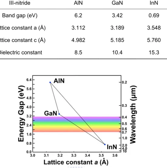
The wurtzite multi-types of GaN, AlN and InN form a continuous alloy system which has direct band gaps range from 0.7 eV for InN, to 3.4 eV for GaN, to 6.2 eV for AlN. Therefore, the III-nitride materials could be very potential to fabricate optical devices which are active at wavelengths ranging from the infrared ray (1550 nm) to ultraviolet (UV) (200 nm). The band gaps and corresponding wavelengths of nitrides are shown in Fig. 1-2 with respect to their lattice constant a [4].
c-plane (0001) m-plane (1100) a-plane (1120) Ga N
Tab. 1-1 Basic material properties of wurtzite AlN, GaN and InN.
III-nitride AlN GaN InN
Band gap (eV) 6.2 3.42 0.69
Lattice constant a (Å) 3.112 3.189 3.548 Lattice constant c (Å) 4.982 5.185 5.760 Dielectric constant 8.5 10.4 15.3
Fig. 1-2 The band gaps of nitrides vs. their lattice constant a.
1-1-2 Milestones for nitride based LEDs
In the history of III-nitride materials, around 1940, GaN binary alloy was first synthesized by Juza and Hahn using passing ammonia over hot gallium, and produced small needles and platelets for the purpose of studying its crystal structure and lattice constant [5]. In 1958, small crystals of GaN were produced with the same technique by Grimmeiss and Koelmans. The first result of photoluminescence (PL) spectra for GaN was demonstrated [6]. During the late 1960s, to create a full color image, the display must contain red, green and blue pixels, Maruska and Tietjen fabricated a large layer of GaN
grown on sapphire (Al2O3) substrate by using chemical vapor deposition technique was demonstrated [7]. As regarding the fabrication of GaN-based LED devices, the first demonstration was reported by Pankove et al. in 1971 [8]. This was the first current-injected GaN light emitter which emitted green and blue light. However, the early works were eventually questionable because of the lack of advanced epitaxial technique and fundamental material problems. To date, sapphire has become the most popular used substrate for the growth of III-nitride materials. This substrate has several advantages such as cheaper than SiC, high hardness, high heat-resistance, and particularly the free of absorption for green, blue, and ultraviolet photons. Despite these advantages, the material structural problem is the main issue when using sapphire as the substrate for nitride growth; as shown in Fig. 1.2, the lattice constant a of GaN is about 3.189 Ǻ with an energy bandgap of 3.39 eV. The interface between GaN and sapphire substrate exists a large lattice mismatch of 15%, causing a very high dislocation density [9, 10]. In addition, sapphire is a dielectric material, both n and p contacts shall be grown on top of the devices, and etching techniques are inevitably required. Therefore, even the sapphire can be the substrate for growing III-nitride materials, the noticeable lattice mismatch and poor crystal quality, obstacle the early development of III-nitride LEDs.
This high dislocation density problem in nitride system was not solved until 1983. Yoshida et al. proposed to improve the crystal quality of GaN film using AlN-coated sappire substrate [11]. Consequently, high-quality GaN thin films with smooth surface had been successfully grown by using AlN nucleation buffer layer with MOCVD technique by Akasaki et al. [12]. In 1991, S. Nakamura used low-temperature amorphous GaN thin films instead of AlN thin
film as new nucleation layer, and mirror-like GaN thin films were obtained under high-temperature growing [13].
Nevertheless, the high n-type background doping in intrinsic GaN film also causes a incapable issue in fabricating GaN p-n junction LEDs since a p-n junction is necessary for semiconductor devices., It could be easily achieved to obtain n-type GaN with an n-doping level of 1×10¹⁷ ~ 2×1019 cm-3 by Si or Se dopant atoms. In contract, for forming p-type GaN layer, even various types of acceptor atoms including Mg and C were tried, it only led to compensated high resistivity material. Until 1989 this bottleneck was first broken through by Akasaki et al. using low energy electron beam irradiation treatment [14]. High quality of GaN thin film with a hole concentration of 1×10¹⁷ and a low resistivity of 12 Ω·cm were obtained.Three years later, the Mg-doped GaN with p-doping level of 3×1018 cm-3 and a resistivity of 0.2 Ω·cm was grown which is more conductive by Nakamura who used a treatment of thermal annealing in a N2 ambient [15].
High-brightness GaN-based blue LEDs need high-quality InGaN films as active layers. In 1990s, a blue InGaN/GaN double-heterostructure LED was first time fabricated by Nakamura. By using two-flow MOCVD technique, the substrate was heated up to 1050 oC in a stream of hydrogen for thermal cleaning. Then the temperature was lowered down to 510 oC for the growth of GaN nucleation layer. Afterward, the substrate was reheated to 1020 oC to grow 4-µm n-type GaN film, followed by the 20-nm-thick Si-doped InGaN active layer at 800 oC. The temperature was then increased to 1020 oC to grow p-type Mg-doped GaN film. The total thickness of structure was about 4.8 µm, and the surface of p-type GaN was partially etched until the n-type layer was exposed. Finally, a Ni–Au metal contact was evaporated onto the p-type GaN
layer and a Ti–Al metal contact was deposited onto the n-type GaN layer. The peak wavelength was 440 nm with a full width at half maximum (FWHM) of 20 nm under injective forward current of 20 mA [7].
The first candela-class blue LEDs were fabricated with the use of Si and Zn codoped InGaN active layer. The InGaN layer with low indium composition was used because of high-indium InGaN layer might degrade luminescence intensity. The thickness of InGaN active layer was 50 nm, and the active layer was sandwiched between two 150-nm-thick Al0.15Ga0.85N cladding layers. The output power and external quantum efficiency at 20 mA were 1.5 mW and 2.7% [16]. Subsequently, the InGaN/InGaN multiple quantum wells (MQWs) structures and several novel designs were employed in GaN-based LEDs. The first commercial GaN-based LEDs were sold by Nichia Chemical Company in 1990s. To date, it is less than fifteen years that high-brightness GaN-based LEDs have been used all over the world, for example, in the applications of full-color displays, traffic signals, other promising areas of high-definition DVD optical storage, chemical processes, and medical applications [17–19].
III-nitride materials are very special. They are the best candidate for short wavelength emission due to their wide and direct energy bandgap. Unlike the arsine or phosphide materials, so far there is no any suitable substrate for nitride growth. In addition, they are in the hexagonal (wurtzite) crystal system. Therefore, the polarization effect in nitride materials has been found much stronger than other III-V compounds [20]. In next section, the material properties of wurtzite GaN and its relevant alloys are discussed.
1-1-3 Spontaneous and piezoelectric polarizations
semiconductors, one is spontaneous polarizationP and the other one is sp
strain-induced polarizationPpiezo. Comparing to other semiconductor materials,
c-face nitride-based materials have much stronger polarization effects [20].
Polarization effect results in separation of wave functions of electrons and holes in the quantum well, as indicated in Fig. 1.3. The transition energy is reduced by the built-in field, leading to a red-shift of the emission wavelength. The thicker the quantum well thickness, the more separated electrons and holes, and the less overlap of electron and hole carrier density distributions, which leads to a smaller recombination rate and lower luminescence efficiency.
Fig. 1-3 Band edges of conduction and valence bands.
A way to estimate the interface charge density has been developed by Fiorentini et al. [21]. The spontaneous polarization of nitride alloys can be expressed by: ) 1 ( 071 . 0 ) 1 ( 042 . 0 090 . 0 ) ( ) 1 ( 038 . 0 ) 1 ( 034 . 0 042 . 0 ) ( ) 1 ( 019 . 0 ) 1 ( 034 . 0 09 . 0 ) ( 1 1 1 x x x x N In Al P x x x x N Ga In P x x x x N Ga Al P x x sp x x sp x x sp − ⋅ ⋅ + − ⋅ − ⋅ − = − ⋅ ⋅ + − ⋅ − ⋅ − = − ⋅ ⋅ + − ⋅ − ⋅ − = − − − (1-1)
2 2 2 2 559 . 7 373 . 1 ) ( 541 . 9 918 . 0 ) ( 0 888 . 7 808 . 1 ) ( 0 624 . 5 808 . 1 ) ( ε ε ε ε ε ε ε ε ε ε ⋅ + ⋅ − = ⋅ + ⋅ − = > ⋅ − ⋅ − = < ⋅ + ⋅ − = InN P GaN P for AlN P for AlN P pz pz pz pz (1-2)
where ε is the in-plane strain of the binary compound considered. Linear interpolation formula is used for the calculation of ternary and quaternary nitride alloys. The total built-in polarization is the sum of spontaneous and piezo-electric polarizations.
1-2 Historical review of nonpolar GaN growth
1-2-1 Material characteristics of nonpolar GaN
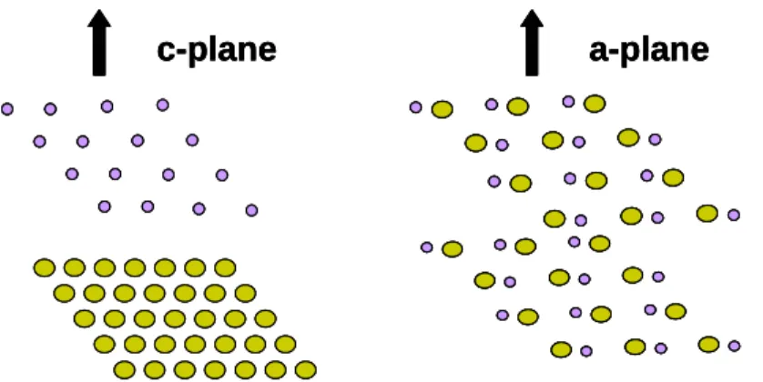
Quantum confined Stark effect (QCSE) typically exists in MQWs structure especially in III-nitride system which causes build-in electric filed and degrades excitons recombination rate [22]. To eliminate QCSE, the nonpolar crystal orientations including a-axis and m-axis have been developed. The monolayer schematic of atomic distribution in c-plane GaN and nonpolar GaN are shown in Fig. 1-4 respectively. Hence, polarization discontinuities exist along the growth direction and create fixed sheet charges at surfaces and interfaces in nonpolar structure. The total polarization of III-nitride film consists of spontaneous and piezoelectric polarization contributions. These resulting internal electric fields would bend the potential band and spatially separate electron and hole wavefunctions in potential wells. According to the schematic of Fig. 1-3, this phenomenon would reduce carrier recombination、red-shift emission and decreased internal quantum efficiency. These effects are manifestations of the QCSE and have been thoroughly analyzed for GaN/ (Al,Ga)N quantum wells.
Fig. 1-4 The monolayer schematic of atomic distribution in c-plane GaN and a-plane GaN.
When commercial LEDs grown on c-plane sapphire had got to be mature gradually in market, Domen et al. used molecular beam epitaxy to grow m-plane GaN on SiC [23]. The optical properties and polarization effect were first revealed shown in Fig. 1-5. They found m-plane GaN could emit polarized light emission due to different amount of excitons recombined between different energy levels.
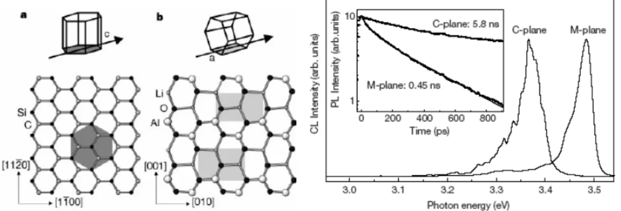
In 2000, Walterelt et al. grew m-plane GaN/ AlGaN MQWs structure on r-LiAlO2 substrate [24]. The relationship between GaN and LiAlO2 is illustrated in left of Fig. 1-6. They used time-resolved photoluminescence (TRPL) to estimate the life time of excitions existed in nonpolar MQWs structure. The life time of excitons in m-plane MQWs was averagely much decreased to 0.45 nm which is much shorter than 5.8 ns of c-plane MQWs. Therefore, they expected this kind of material could be used for advance white light source.
Most groups focused on nonpolar III-nitride concentrated their effort on growth condition, structural characteristics and polarization effect. However, the first time to demonstrate no build-in electric field in nonpolar structure is in 2002 which was carried out by Kuokstis et al. using power dependent PL to confirm and observe exist of internal electric field [25]. Since c-plane MQWs
c-plane a-plane
c-plane
possess internal electric field, the plenty injected carriers would produce an opposite electric field in well and thus cause a blue-shift PL emission due to screen effect, whereas screen effect didn’t happen in nonpolar MQWs.
Fig. 1-5 PL spectra of m-plane GaN under different polarized angle measurements. (Appl. Phys. Lett., 71, 1996, 199)
In addition, since the growth direction of either m or a-plane GaN is perpendicular to that of traditional c-plane GaN, the hetero-epitaxial growth of nonpolar GaN always suffers biaxial stress comes from different crystal orientations. For example, the epitaxial relationships between a-plane GaN and r-plane sapphire are found to be [1100]GaN||[1120]sapphire and [0001]GaN||[1101]sapphire, respectively [26, 27]. Therefore, most groups believe this complicated relationship results in difficulty of nonpolar GaN growth so that the key point to develop nonpolar nitride based devices is the improvement of nonpolar GaN crystal quality.
To sum up all above descriptions, nonpolar GaN has following advantages including: free of internal electric field, high degree of polarization and expected high performance of optoelectronic devices. On the other hand, the asymmetrical strain comes from biaxial stress will be a critical issue which would make epitaxy growth difficult. Next section the growth of nonpolar GaN
will be discussed. The relevant characteristics of nonpoplar GaN in different growth approaches will also described.
Fig. 1-6 Left image is the structural characterizations of hexagonal GaN grown on r-LiAlO2.
1-2-2 Growth of nonpolar GaN
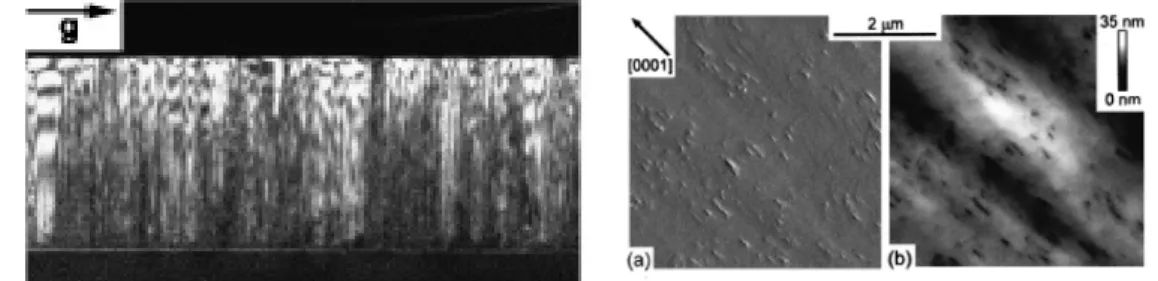
There are many techniques to grow nonpolar GaN including MOCVD, MBE and halide vapor phase epitaxy (HVPE) which are well-known and common techniques. Craven et al. at University of California in Santa Barbara (UCSB) studied the material properties of a-plane GaN on r-plane sapphire grown using MOCVD [28]. This debut revealed the threading dislocations (TDs) density is about 2.6×10¹⁰
cm-2 which is much higher than the order of 107 ~108 cm-2 exist in c-plane GaN/sapphire system. In addition, the plenty stacking faults (SFs) density were also found. Surface morphology of a-plane GaN was also rough observed by atomic forced microscopy (AFM). As Fig. 1-7 left transmission electron microscopy (TEM) image and right AFM images, they suspected that plenty TDs penetrated surface and then produced pits. Since defects have the ability to trap carriers which generate radiative emission, a-plane GaN thin film can’t obtain excellent optical efficiency even though nonpolar MQWs structure has better recombination rate of excitons than
c-plane MQWs has in theory.
Fig. 1-7 TEM and AFM images of a-plane GaN grown on sapphire. (Appl. Phys. Lett., 81, 469, 2002)
Rau et al. grew m-plane GaN/ AlGaN MQWs by using MBE [29]. They confirmed polarization characteristics of nonpolar MQWs structure which revealed the strongest intensity could be obtained when electric field is perpendicular to c-axis of unit hexagonal cell. They also observed that surface morphology has tiny stripes, which is another main feature of nonpolar nitride materials [30]. Their partial results are shown in Fig. 1-8.
Fig. 1-8 Left is the schematic of radiative emission of m-plane GaN/AlGaN MQWs and PL spectra; Right is the AFM image which shows the surface morphology of m-plane GaN. (Appl. Phys. Lett., 77, 3343, 2000/ J. Crys. Grow. 227-228, 437, 2001)
Craven et al. used lateral over growth (LEO) method which was used for improvement of c-plane GaN crystal quality to reduce TDs density in a-plane
GaN [31]. SiO2 layer of 200 nm was deposited on GaN, afterward, they defined the stripe pattern with different directions using lithography technique. The GaN stripes were grown like the image of Fig. 1-9. The TDs density in each stripe was reduced especially in (1100) direction. Therefore, LEO method is one of approaches to improve crystal quality of a-plane GaN. In 2003, this group proposed using nanorods structure as template to improve a-GaN crystal quality [32]. They found the as-grown GaN has better crystal quality using 50 um height nanorods. Fig. 1-10 shows the AFM images with/ without using this technique. Apparently, the typical stripe feature was still shown up but the better surface morphology was really obtained using nanorods technique.
Fig. 1-9. a-plane GaN stripes along different directions using LEO. (Appl. Phys. Lett., 81, 1201, 2002.)
Fig. 1-10. AFM images of surface morphology of a-plane GaN grown on (a) nanorods structure and (b) regular GaN. (Appl. Phys. Lett., 83, 2599, 2003)
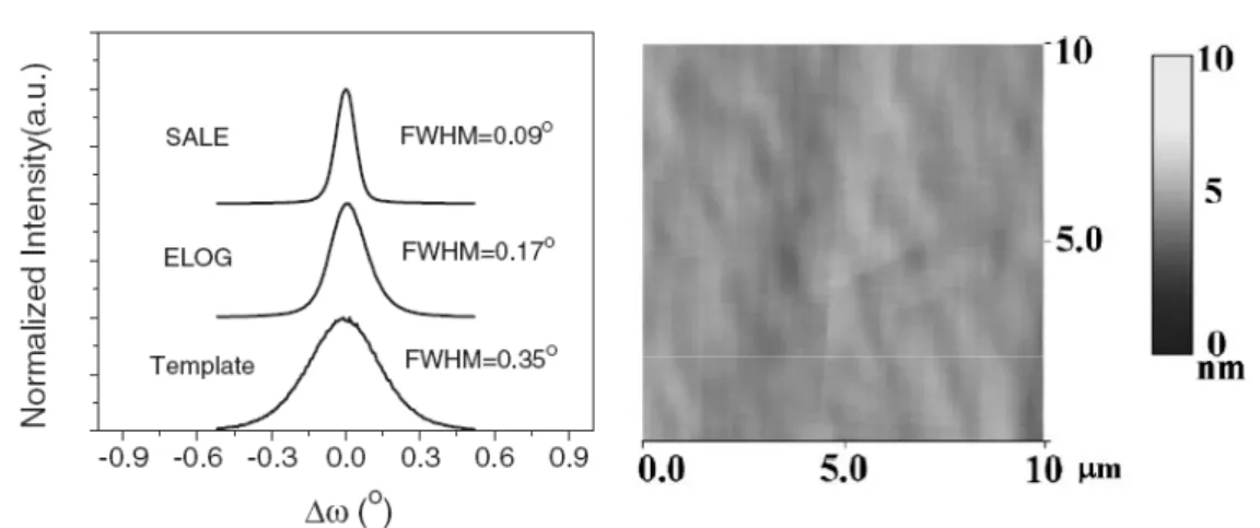
In addition to using nanorods structure as catalyst for LEO technique, Chen et al. also developed selective area lateral epitaxy approach (SALE) [33]. Using GaN with high depth-width ratio etched by lithography, following grown by SiO2 thin layer of 300 nm for passivation. Finally they placed this sample into MOCVD reactor for further growth. As the results of scanning electronic microscope (SEM), Fig. 1-11, SALE technique reduced plenty TDs down to about 107cm-2. X-ray diffraction (XRD) shows the ability of improvement is better to compare to epitaxial lateral overgrowth (ELOG). AFM image also revealed this kind GaN has mirror-like surface. The relevant results are also included in Fig. 1-12.
Fig. 1-11. SEM cross section image of a-plane GaN grown using SALE technique. (Jpn. J. Appl. Phys., 42, L818, 2003)
Fig. 1-12. Left image investigated crystal quality of a-plane GaN grown using different techniques examined by XRD analysis. (Jpn. J. Appl. Phys. 42, L818,
2003)
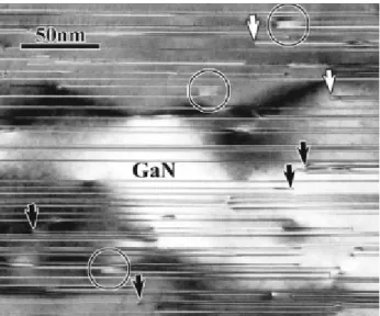
Wu et al. published one paper in Journal of Applied Physics which investigated the growth of a-plane GaN on r-plane sapphire in 2003 [34]. They took many methods related to analyses of material property to examine the difficulty of growth of a-plane GaN. They observed the different growth rates along m-axis and c-axis. In addition, the growth rate of Ga-polar is about four times to that of N-polar. Therefore, it is hard to get smooth surface and well crystallization of a-plane GaN. The typical V-defect occurred in c-plane GaN which is turned into another feature called <-defect composed of two tilt {1011} as Fig. 1-13 shown. In the same year, 50 um thick GaN film was demonstrated and grown by using HVPE [35]. However, the above problems still can’t be ruled out after further TEM observation. TDs density is about 2×10¹⁰
cm-2. The TEM images are shown in Fig. 1-14.
Since nonpolar unique material properties, to develop and grow materials and devices relating to a-plane GaN are very difficult. To use ELOG technique would be complicated and cost-consuming. So far a lot of groups are engaging in develop several ways to improve crystal quality of nonpolar GaN. Akasaki et
Fig. 1-14. TEM images of a-plane GaN grown by HVPE. (Appl. Phys. Lett., 83, 1554, 2003)
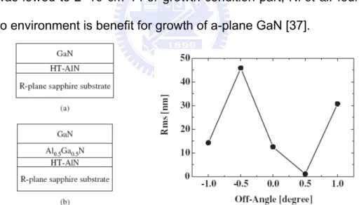
al. try to using double buffer layers to alleviate the problem of lattice mismatch
between a-plane GaN and r-plane sapphire, the structure is shown in Fig. 1-15 [36]. In addition, they tried to grow a-plane GaN on off-cut r-plane sapphire. The results revealed the best surface obtained when using 0.5 degree off-cut r-plane sapphire. The TDs density was reduced down to 5.5×109cm-2, the SFs densitywas lowed to 2×105cm-1. For growth condition part, Ni et al. found low V-III ratio environment is benefit for growth of a-plane GaN [37].
Fig. 1-15 The structural design in left figure and the results using r-plane sapphire with different off-cut angles. (Jpn. J. Appl. Phys. 44, 7418, 2005)
Recently, DenBaars et al. proposed using SiNx layer as nanomask to block TDs [38]. Their experiments demonstrated TDs density was reduced to 9×109cm-2 and SFs density was reduced to 3×105 cm-1, respectively. Fig. 1-16
shows their AFM results. The detailed observation results are shown in Tab. 1-2.
Fig. 1-16. AFM images of a-plane GaN surface (a) without (b) with SiNx nanomask. (Appl. Phys. Lett., 89, 041903, 2006)
Tab. 1-2. Summary of TEM results related to a-plane GaN using SiNx nanomask. (Appl. Phys. Lett., 89, 041903, 2006)
1-2-3 Nonpolar GaN applications
In theory, nonpolar optoelectronic devices should have excellent performance and have higher internal quantum efficiency than conventional c-plane devices have. However, that a bunch of defects exist in nonpolar nitride materials results in poor light extraction efficiency of optoelectronic devices. In spite of that, the possibility to fabricate a high efficient optoelectronic device is very attractive to many scientists over the world. Under this expectation, many groups have developed nonpolar GaN based optoelectronic devices including mainly nonpolar LEDs and laser diodes (LDs).
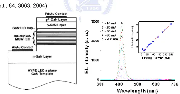
First nonpolar LED chip was fabricated in 2004 by Chitnis et al. [39]. In order to avoid production of plenty defects in a-plane GaN structure lead to low
performance of LED so that they grew a pretty thick n-type GaN layer of 30 µm. The structure design and spectra results are shown in Fig. 1-17. The spectrum results revealed a unusual blue-shift peak with increasing injection current. They attributed band filling and screen effect [40].
Fig. 1-17. Left schematic is the structure of first a-plane LED; right figure shows the luminescence spectra with different injection currents. (Appl. Phys. Lett., 84, 3663, 2004)
Fig. 1-18. Left figure is the designed structure of a-plane blue LED using ELOG technique. Right figure is the spectrum results with different currents. (Appl. Phys. Lett., 85, 5143, 2004)
LED which reduced much defects, the structure of LED and it’s performance are shown in Fig. 1-18 [40]. The highest power was about 240 µW at 20 mA, the external quantum efficiency (EQE) is about 0.4 %. Furthermore, the power was 1.5 mW when 250 mA current was injected. The forward voltage was about 3.3 V and series resistance was about 7.8Ω. In addition, the emission didn’t shift under different injection currents.
Because of much defects generation from heterostructure interface between GaN and sapphire, many groups started to select free standing a-plane GaN as substrate to resolve this problem. Chakraborty et al. also successfully grew m-plane LEDs with typical structure on free standing m-plane GaN substrate in 2005 [41]. The procedure of using directly free standing substrate is totally easier than using ELOG technique. On that time, the power of LED can reach 2.95 mW at 300 mA and the turn on voltage is about 3~4 V which is similar to the previous result mentioned using ELOG technique [40]. In addition, The EQE can reach 40 %. The structure and performance of this LED are shown in Fig. 1-19.
Fig. 1-19 Left figure shows the typical structure of LED grown on free standing substrate; right figure is the output power of this device as a function of drive current. (Jpn. J. Appl. Phys. 44, L173, 2005)
The first continuous-wave operation of nonpolar LDs with lasing peak approximately 400 nm was fabricated and grown on m-plane free standing GaN by Okamoto et al. in 2007 [42]. The threshold current was 36 mA which is comparable to that of conventional c-plane LDs. They fabricated different LDs along c-axis and m-axis, the results of Fig. 1-20 pointed out that c-axis stripe LDs exhibited lower threshold current density since the lowest energy transition is allowed. Fig. 1-20 also revealed the regular LDs structure design of nonpolar LDs.
Fig. 1-20 Schematic of the LDs with the stripe parallel to c-axis in left figure; L-I characteristics of c- and a-axis stripe LDs in right figure. (Jpn. J. Appl. Phys. 46, L173, 2005)
In the same year, Feezell et al. proposed AlGaN-cladding free structure of nonpolar LDs and further demonstrated this possibility [43]. The pulsed lasing mode can be operated with threshold voltages and current densities of 6.7 V and 3.7 kA/ cm2, respectively. The same group also demonstrated a high power and external efficiency m-plane blue LEDs grown on bulk m-plane GaN substrates using MOCVD [44]. The output power and EQE of packaged 300 X 300 µm2 was 23.7 mW and 38.9 % at 20 mA, respectively.
To sum up above description, during the last few years, and extensive research activity, related to growth and characterization of the nonpolar nitride material system has studied worldwide. Fig. 1-21 depicts the publication record in the scientific journals indicating the strong increase of interest in
nonpolar nitride research. Despite high-efficiency nonpolar LEDs and LDs have been demonstrated using free standing nonpolar GaN substrate, so far it is hard to get a high quality nonpolar free standing GaN substrate so that this development still can’t make a progress in commercial market and other applications. Using GaN substrate is very expensive which add the difficulty to fabricate nonpolar optoelectronic devices. Therefore, to seek a good epitaxial technique and figure out the mechanism of nonpolar GaN growth are necessary for nonpolar development road. A better understanding of the specific features, properties and challenges in both growth and characterization of this material system is also required.
Fig. 1-21 The number of publications peryear focused on nitrides with polar, nonpolar and semipolar surfaces versus time.
1-3 Challenges to grow nonpolar GaN based LEDs
1-3-1 Morphology
The most commonly observed features of thin nonpolar nitride layer grown by both MOCVD and MBE techniques is striated. It is also called slate morphology, dominated by ridges with orientations, that appeared to be along
1965 1970 1975 1980 1985 1990 1995 2000 2005 2010 1 10 100 1000 GaN Timeline Total P ublications (P er Y ear) Calendar Year GaN Nonpolar Semipolar
a-axis in the m-plane GaN films grown on (100) LiAlO2 [45, 46], and along the c-axis in the a-plane GaN films grown on r-plane sapphire [47]. Many studies of the substrate morphology revealed that the stripe pattern follow the corresponding ones of the substrates and it appears that the morphologies of the nonpolar nitrides replicate the substrate morphology.
Conventional c-plane GaN grown by HVPE has hillock-type feature on surface revealed by SEM. Unlike c-plane GaN, the morphology of the thick nonpolar a-plane GaN films is stripe-shaped on a large scale with no perfect stripe orientation. The morphology of a-plane GaN layers was often reported as decorated by triangle pits. They were observed in films grown by different techniques which have been regarded as a typical surface defects under nonoptimized growth condition. The morphology was shown in Fig. 1-13. Based on previous description, Wu et al. revealed that the surface pits are indeed parts of three dimensional hexagonal pyramids lying in the growth plane with the tips pointing to the c-axis [34]. Therefore, the facets opposite to the tips are vertical, coinciding with the c-plane and forming an N-face wall. It is more like well-known V-type defects in c-plane GaN. This specific features of the morphology of the nonpolar heteroepitaxial films are directly related to the microstructure, such like both point and structural defects. These problems related to surface will obstacle the further structural growth of MQWs or LEDs.
1-3-2 Threading dislocations & Stacking faults
The heteroepitaxially growth of nitrides have always encountered a huge defect density. In fact, the biggest problem for crystal quality development of the nonpolar nitrides is their microstructure. Both TDs and SFs were found in nonpolar thin film. The TDs and SFs are deteimental for the lifetime of such
devices because they act as current shortcut pathways. In several reviews on the microstructure of nonpolar nitride films grown either on r-plane sapphire, a-plane SiC or LiAlO2 substrates, the TDs are reported to have densities in the range of 1010 cm-2 and SFs in the range of 105 cm-1. Different types of SFs have been revealed in the nonpolar GaN films by TEM [48]. The dominating defects were basal plane SFs, being bonded by two partial dislocations which are in accordance with the theory, which is shown in Fig. 1-22. Since the TDs and SFs originate at the interface between the substrate and film, the character of the misfit dislocations in the a-plane GaN have been evaluated by conducting detailed studies of the atomistic structure of the interface. The SFs induce built-in electric field along c-axis, with a magnitude roughly proportional to the density of SFs [49], causing in-plane carrier separation and junction leakage current [41], offsetting the benefits of nonpolar growth. Therefore, a further fully knowledge of these properties is of critical importance to understand the defect forming mechanisms in the early stages of the nonpolar GaN growth to be able to control, reduce and avoid their formation.
Fig. 1-22 Bright field TEM images of a plan-view sample parallel lines represent SFs formed on the basal plane of GaN. (Phys. Rev. B 71, 235334 (2005))
1-4 Motivation
Because above description about the difficulties of heteroepitaxy of nonpolar GaN either on r-plane sapphire or r-AlLiO2, herein we concentrated our effort on the growth of high quality a-plane GaN with free pits on r-plane sapphire in the earlier stage of this work. The optimum growth of a-plane GaN grown on sapphire by MOCVD was investigated. The suitable growth condition for a-plane GaN was also confirmed, including growth temperature, pressure, and V/III ratio. In addition, we try to use Wulff-plot concept to figure out the growth mechanism and the pits origin of a-plane GaN by using selective area growth method. This relevant works will be discussed in Chapter 3 and 4. In order to reduce a plenty defects exist in a-plane GaN layer, we proposed two reliable and useful methods. First one is trench epitaxial lateral overgrowth (TELOG) and the other one is the use of InGaN/GaN superlattices (SLs). Both of two methods are low cost and time-saving in comparison to some ways like using free standing nonpolar GaN substrate or ELOG. We investigated the effect of using these two approaches on the improvements of crystal quality and other fundamental material properties. The detailed report will be summed up in Chapter 5.
Before fabrication of nonpolar LEDs, we still need to examine the optimum structure of MQWs by adjusting different well width even though electric field free in nonpolar direction. The a-plane InGaN/GaN MQWs with different well widths were grown by MOCVD. By using CL and TRPL analysis, we can conclude the influence of MQWs with different well widths on carrier dynamic, recombination rate and localization degree in a-plane MQWs structure. The suitable condition for emission efficiency will be revealed and applied in further fabrication of a-plane LEDs.
Eventually, we utilized and applied previous knowledge and experimental results to grow high quality a-plane GaN template for further LEDs structure. The design of InGaN/GaN MQWs structure reported in previous work is adopted. Basic electrical and optical properties of a-plane LEDs were carried out and other relevant phenomenon were also observed and explained in Chapter 7. A series of experiments demonstrate that nonpolar LEDs is potential and capable of application of solid state lighting in future.
Reference
[1] M. J. Paisley, 2. Sitar, J. B. Posthil, and R. F. Davis, J. Vac. Sci. Tech. B 7, 701 (1989).
[2] J. I. Pankove, S. Bloom, and G. Harbeke, RCA Rev. 36, 163 (1975).
[3] H. Morkoç, “Nitride Semiconductors and Devices”, Springer, 1998, Virginia.
[4] E. Fred Schubert, “Light-Emitting Diodes”, Cambridge, 2006, New York. USA.
[5] R. Juza, H. Hahn, Z. Anorg. Chem. 239, 285 (1938).
[6] H. G. Grimmeiss, H. Koelmans, Zeitschrift Naturforschung Teil A 14, 264 (1959).
[7] G. B. Stringfellow, and M. G. Craford, “High Brightness Light Emitting Diodes: Semiconductors and Semimetals Volume 48,” Academic Press, San Diego, California, USA (1997).
[8] J. I. Pankove, E. A. Miller, J. E. Berkeyheiser, J. Luminescence 5, 84, (1972).
[9] S. D. Lester, F. A. Ponce, M. G. Craford, and D. A. Steigerwald, Appl. Phys. Lett. 66, 1249, (1995).
[10] S. Chichibu, T. Azuhata, T. Sota, and S. Nakamura, Appl. Phys. Lett. 69, 4188, (1996).
[11] S. Yoshida, S. Misawa, and S. Gonda, Appl. Phys. Lett. 42, 427, (1983). [12] H. Amano, N. Sawaki, I. Akasaki, Y. Toyoda, Appl. Phys. Lett. 48, 353,
1986.
[13] S. Nakamura, Y. Harada, and M. Seno, Appl. Phys. Lett. 58, 2021, (1991). [14] H. Amano, M. Kito, K. Hiramatsu, and I. Akasaki, Jpn. J. Appl. Phys. 28,
[15] S. Nakamura, T. Mukai, M. Senoh, and N. Iwasa, Jpn. J. Appl. Phys. 31, L139, (1992).
[16] S. Nakamura, IEEE J. Sel. Top. Quantum. Electron. 4, 483, (1998).
[17] J. Piprek, “Nitride Semiconductor Devices,” WILEY-VCH Verlag GmbH & Co. KgaA, Weinheim (2007).
[18] G. O. Mueller and R. Mueller-Mach, “Set The Pace in White Space–White LEDs for illumination and Backlighting,” Proceedings of Intertech Phosphor Global Summit, San Diago, 2005.
[19] M. Kurata, “Numerical Analysis for Semiconductor Devices,” D.C. Health & Company, Lexington Massachusetts, 1982.
[20] F. Bernardini, V. Fiorentini, and D. Vanderbilt, Phys. Rev. B, 56, R10024, (1997).
[21] V. Fiorentini, F. Bernardini, and O. Ambacher, Appl. Phys. Lett. 80, 1204, (2002).
[22] D. A. B. Miller, D. S. Chemla, T. C. Damen, A. C. Gossard, W. Wiegmann, T. H. Wood and C. A. Burrus, Phys. Rev. Lett. 53, 2173 (1984).
[23] K. Domen, K. Horino, A. Kuramata, T. Tanahashi, Appl. Phys. Lett. 71, 1996, (1997).
[24] P. Waltereit, O. Brandt, A. Trampert, H. T. Grahn, J. Menniger, M. Ramsteiner, M. Reiche, K. H. Ploog, Nature 406, 865, (2000).
[25] E. Kuokstis, C. Q. Chen, M. E. Gaevski, W. H. Sun, J. W. Yang, G. Simin, M. Asif Khan, H. P. Maruska, D. W. Hill, M. C. Chou, J. J. Gallagher, B. Chai, Appl. Phys. Lett. 81, 4130, (2002).
[26] T. Sasaki and S. Zembutsu, J. Appl. Phys. 61, 2533 (1987).
[27] T. Shibata, K. Asai, Y. Nakamura, M. Tanaka, K. Kaigawa, J. Shibata, and H. Sakai, J. Cryst. Growth 229, 63 (2001).
[28] M. D. Craven, S. H. Lim. F. Wu, J. S. Speck, S. P. DenBaars, Appl. Phys. Lett.,81, 469, (2002).
[29] B. Rau, P. Waltereit, O. Brandt, M. Ramsteiner, K. H. Ploog, J. Puls, F. Henneberger, Appl. Phys. Lett. 77, 3343, (2000).
[30] P. Waltereit, O. Brandt, M. Ramsteiner, A. Trampert, H. T. Grahn, J. Menniger, M. Reiche, K. H. Ploog, J. Crys. Grow. 227, 437, (2001).
[31] M. D. Craven, S. H. Lim, F. Wu, J. S. Speck, S. P. DenBaars, Appl. Phys. Lett. 81, 1201, (2002).
[32] W. H. Sun, J. W. Yang, C. Q. Chen, J. P. Zhang, M. E. Gaevski, E. Kuokstis, V. Adivarahan, H. M. Wang, Z. Gong, M. Su, M. Ssif Khan, Appl. Phys. Lett. 83, 2599, (2003).
[33] C. Chen, J. Zhang, J. Yang, V. Adivarahan, S. Rai, S. Wu, H. Wang, W. Sun, M. Su, Z. Gong, E. Kuokstis, M. Gaevski, M. Asif Khan, Jpn. J. Appl. Phys. 42, L818, (2003).
[34] Feng Wu, M. D. Craven, S. H. Lim, J. S. Speck, J. Appl. Phys. 94, 942, (2003).
[35] B. A. Haskell, F. Wu, S. Matsuda, M. D. Craven, P. T. Fini, S. P. DenBaars, J. S. Speck, S. Nakamura, Appl. Phys. Lett. 83, 1554, (2003).
[36] M. Imura, A, Hoshino, K. Nakano, M. Tsuda, M. Iwaya, S. Kamiyama, H. Amano, I. Akasaki, Jpn. J. Appl. Phys. 44, 7418, (2005).
[37] X. Ni, Y. Fu, Y. T. Moon, N. Biyikli, H. Morkoç, J. Crys. Grow. 290, 166, (2006).
[38] A. Chakraborty, K. C. Kim, F. Wu, J. S. Speck, S. P. DenBaars, U. K. Mishra, Appl. Phys. Lett. 89, 041903, (2006).
[39] A. Chitnis, C. Chen, V. Adivarahan, M. Shatalov, E. Kuokstis, V. Mandavilli, J. Yang, M. A. Khan, Appl. Phys. Lett. 84, 3663, (2004).
[40] A. Chakraborty, B. A. Haskell, S. Keller, J. S. Speck, S. P. DenBaars, S. Nakamura, U. K. Mishra, Appl. Phys. Lett. 85, 5143, (2004).
[41] A. Chakraborty, B. A. Haskell, S. Keller, J. S. Speck, S. P. DenBaars, S. Nakamura, U. K. Mishra, Jpn. J. Appl. Phys. 44, L173, (2005).
[42] K. Okamoto, H. Ohta, S. F. Chichibu, J. Ichihara, H. Takasu, Jpn. J. Appl. Phys. 46, L173, (2007).
[43] D. F. Feezell, M. C. Schmidt, R. M. Farrell, K. C. Kim, M. Saito, K. Fujito, D. A. Cohen, J. S. Speck, S. P. DenBaars, S. Nakamura, Jpn. J. Appl. Phys. 46, L284, (2007).
[44] M. C. Schimidt, K. C. Kim, H. Sato, N. Fellows, H. Masui, S. Nakamura, S. P. DenBaars, J. S. Speck, Jpn. J. Appl. Phys. 46, L126, (2007).
[45] B. A. Haskell, A. Chakraborty, F. Wu, Journal of Electronic Materials 34, 357 (2005).
[46] Y. J. Sun, O. Brandt, K. H. Ploog, J. Vac. Sci. Tech. B 21, 1350 (2003) [47] H. Wang, C. Chen, Z. Gong, J. Zhang, M. Gaevski, M. Su, J. Yang, M. Asif
Khan, Appl. Phys. Lett. 84, 499 (2004).
[48] D. N. Zakharov, Z. L. Weber, Phys. Rev. B 71, 235334 (2005).
[49] G. D. Metcalfe, H. Shen, M. Wraback, A. Hirai, F. Wu, and J. S. Speck, Appl. Phys. Lett. 92, 241106 (2008).
C
Ch
ha
ap
pt
te
er
r
2
2
Ex
E
xp
pe
er
ri
im
me
e
nt
n
ta
a
l
l
in
i
ns
st
tr
r
um
u
m
en
e
nt
ts
s
an
a
nd
d
ph
p
hy
y
si
s
ic
ca
al
l
m
mo
od
de
el
ls
s
MOCVD, XRD, all kinds of electronic microscopy and spectra, were widely used for this thesis works, the detailed description of the instruments will be introduced in this chapter. For an excellent epitaxial grower, to understand basic theory and principle of machine is the most important because it could dominate whether crystal quality is perfect or not. In addition, the analyses of material properties are worth being carried out in order to obtain whole material information which can help us evaluate applications. Therefore, the content of this chapter we will mentioned involves system schematic, operation principles and fundamental knowledge.
2-1 Metal organic chemical vapor deposition, MOCVD
MOCVD is currently the most widely used technology for nitride compound semiconductor thin film growth. Actually, most of all optoelectronic commercial device structures are fabricated using MOCVD. Its potentials have been proven by producing high quality epitaxial layers with excellent surface morphology and a precise control over layer thickness and uniformity. Some epitaxial crystal growth technology for an impressive array of commercial devices are also carried out by MOCVD, such like lasers, LEDs, photocathodes, heterostructure bipolar transistors, photodetectors, and solar cells [1-3].
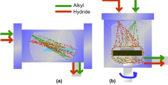
MOCVD growth is facilitated by introducing group III precursors and NH3 with carrier gases into a reactor under appropriate growth temperature and growth processes. In general, a typical MOCVD system consists of four major parts; growth reactor, gas delivery system, heating system, and exhaust system.
I. Main reactor chamber
The reactor system for carrying out CVD processes must provide several basic functions to all types of systems. Most reactants and diluent gases were allowed to move to the reaction site and absorb activation energy while maintaining a specific system pressure and temperature. Moreover, the reactor also allows the chemical reactions for epitaxial film growth optimally and to exhaust out the by-product gases and vapors. These functions must be operated with adequate control, maximal effectiveness, and complete safety. The reaction chamber is more like the heart of human which is connected the vessel, all kinds of source gases are mixed and introduced into a heated zone where an appropriate substrate is placed, and then the basic pyrolysis reactions described above take place. There are two basic MOCVD reaction chamber geometries commonly used for epitaxial III-nitride growth [4, 5]. One is vertical reactor chamber, the other is horizontal one, which are mainly fabricated by famous companies Veeco and Aixtron [6, 7]. For both designs, cold-wall systems are attached which contain a relatively small diameter inlet into some form of transition region and make use of an indirectly heated (filament or radio-frequency induction heated) silicon carbide-coated graphite susceptor. In this thesis, I used Veeco D75 MOCVD with vertical reactor at NCTU, the relevant results will be discussed in further chapter 3, 5, 6 and 7 except for partial content of chapter 5. Aixtron 200 MOCVD was used at Yale
to carry out growth behavior of nonpolar GaN, which will be mentioned in whole chapter 4 and partial chapter 5. Therefore, this understanding in terms of growth behavior of nonplar GaN still will not conflict with other results.
Fig. 2-1 (a) Horizontal reactor and (b) vertical reactor in MOCVD system. In the horizontal reaction chamber is shown in Fig. 2-1(a), the precursors and gases enter from the small inlet to the left and expand to an approximately laminar flow across the heated susceptor. Whole 2 inch wafer or small pieces can be accommodated along the length of the susceptor, or be placed side by side if the susceptor area is large enough. Hydrogen flow from the bottom side can flow in the special designed pattern on the down side of puck and lead to rotation of puck. In contrast, in the vertical reaction chambershown in Fig. 2-1 (b), the process gases enter at the top and are deflected by a baffle before moving downward through a cold transition region and approaching normal to the heated susceptor. The gas flow is forced to the sides by the susceptor with a velocity profile dependent on geometry and affected by the thermal profile in the system. Uniformity could be improved by rotating the susceptor. Exhaust gases escape through the base of the reaction chamber. 2 inch water is allowable for growth but small pieces can not be loaded on susceptor due to