國 立 交 通 大 學
顯示科技研究所碩士班
碩士論文
銅製程對非晶矽氧化銦鎵鋅薄膜電晶體
特性影響之研究
Study on the effects of copper process on the
a-IGZO thin film transistor
研 究 生: 李承旻 Cheng-Min Lee
指導教授: 戴亞翔 博士 Dr. Ya-Hsiang Tai
銅製程對非晶矽氧化銦鎵鋅薄膜電晶體
特性影響之研究
Study on the effects of copper process on the
a-IGZO thin film transistor
研 究 生 : 李承旻 Student: Cheng-Min Lee
指導教授 : 戴亞翔 博士 Advisor: Dr. Ya-Hsiang Tai
國立交通大學
顯示科技研究所碩士班
碩 士 論 文
A Thesis
Submitted to the Display Institute
College of Electrical and Computer Engineering
National Chiao Tung University
in Partial Fulfillment of the Requirements
for the Degree of Master
in
Display Institute
Feb 2013
Hsinchu, Taiwan, Republic of China
銅製程對非晶矽氧化銦鎵鋅薄膜電晶
體特性影響之研究
學生:李承旻 指導教授:戴亞翔 博士
國立交通大學顯示科技研究所碩士班
摘要
在這份研究裡,將探討銅製程對非晶矽氧化銦鎵鋅(a-IGZO)薄膜電晶(TFTs) 特性的影響。我們藉由比較電極為鈦/鋁/鈦結構的薄膜電晶體和電極為銅/鈦結 構的薄膜電晶體特性,觀察到銅/鈦結構的薄膜電晶體特性會產生惡化,以及偏 壓加壓下的不穩定性會增加。藉由二次離子質譜分析儀得知此現象是因為銅進入 元件的通道層。為了探討銅的濃度對非晶矽氧化銦鎵鋅薄膜電晶體特性影響的關 係,我們將鈦/鋁/鈦結構的薄膜電晶體浸泡在硫酸銅溶液中,以觀察對元件影響 的程度,及其內部缺陷的變化。本研究充分證明銅對薄膜電晶體的影響,足為使 用銅製程製作 a-IGZO TFTs 的重要參考。Study on the effects of copper process on
the a-IGZO thin film transistor
Student:Cheng-Min Lee Advisor:Dr. Ya-Hsiang Tai
Display Institute,
National Chiao Tung University
Abstract
In this work, the influence of copper process on amorphous type Indium Gallium Zinc Oxide (a-IGZO) thin film transistor’s (TFTs) transfer curve is studied. By comparing the TFTs characteristics with Ti/Al/Ti source/ drain and Cu/Ti source/drain, we observed that the performance of Cu/Ti structure would become worse than that with Ti/Al/Ti structure. Furthermore, the bias stress induced instability would become more obvious. It is attributed to the presence of the copper in the channel region of the device, which is verified by Secondary Ion Mass Spectrometry (SIMS) analysis. In order to check the influence of Cu, a verification experiment is conducted by dipping Ti/Al/Ti structure devices into the solution of CuSO4. With this experiment, we can observe the influence o f Cu with different
concentration on change of density of states (DOS). This study substantially proves the influence of copper on the characteristics of TFT, which is an important reference for the fabrication of a-IGZO TFT using Cu process.
Acknowledgements
在研究生學習生涯中,最感謝的是我的指導老師 戴亞翔博士,老師對我的 影響不論是在研究上或是生活上都給予了我豐富的教導,讓我受益良多。此外, 老師對於我的個性多所容忍並給予我適當的建議,使我對於未來的生活能夠有一 個明確的方向。感謝老師總是不厭其煩的提醒我、指導我,並且在我的研究上提 供了許多的想法,讓我受益良多。在此,對我敬愛的老師致上最誠摯的謝意。 此外,感謝一路指導我的學長皓麟,為我做了那麼多的幫助,對你真的感到 很抱歉,祝福你未來的路上一切順利。感謝祿盛學長及其他的學弟,在我有所困 難時協助我度過難關。 最後,感謝我的家人,總是在背後默默的支持和鼓勵,給予我高度的肯定, 有了你們的幫助,才讓我能好好的完成碩士學位,在此向你們送上最真摯的感謝。 承旻 2013.02.21Contents
Chinese Abstract………...……...I
English Abstract...II
Acknowledgements... III
Contents ... IV
Table Captions... VI
Figure Captions ...VII
Chapter 1: Introduction…….……….…………1
1.1 Overview and Background……..……….….………..1
1.2 Motivation ………..….…4
1.3 Thesis Organization………..5
Chapter 2: Experimental Parameters and Process………..…….9
2.1 Procedures of Fabricating a-IGZO TFTs………..………9
2.2 Extraction of Device Electrical Parameters………..9
2.2.1 Determination of the Threshold Voltage (VT H)...10
2.2.2 Determination of the Sub-threshold Swing (SS.) ...10
2.2.3 Determination of the Parasitic Contact Resistance……….10
2.2.4 Determination of the Density of States (DOS) ...11
Chapter 3: Bias Stress Induced Instability………..………...….15
3.1 Bias Stress Mechanism...15
3.2 Positive Bias Stress (PBS) ...16
3.2.1 Stress Condition……...16
3.2.2 PBS Results...17
3.3 Negative Bias Stress(NBS) and Negative Bias Illumination Stress(NBIS)...17
3.3.1 Stress Condition...17
3.4 DOS Change after Bias Stress...19
Chapter 4: Copper Induced Instability
...284.1 Ti/Al/Ti vs. Cu/Ti Comparison...28
4.2 Ti/Al/Ti+CuSO4 Solution Dipping...29
4.3 DOS Discussion...30
Chapter 5: Conclusions and Future Work………..…...……..42
Table Captions
Chapter 1
Table 1.1 Comparison of different TFT technologies………...4
Chapter 3
Table 3-1 Experiment conditions of PBS stress.………...16 Table 3-2 Experiment conditions of DC stress..………...18
Figure Captions
Chapter1
Fig 1.1(a) Schematic orbital drawing of electron conducting pathway (conduction
band bottom) in conventional covalent bond semiconductors (e.g. Si)……7
Fig 1.1(b) Schematic orbital drawing of electron conducting pathway (conduction band bottom) in ionic oxide semiconductors……….7
Fig 1.2 Absorption spectrum of the a-IGZO thin film transistor………8
Fig 1.3 Developing trend of a-IGZO TFT display in the world………....8
Chapter 2
Fig 2.1 Physical origin of the resistance components in Eq. (1)………..13Fig 2.2 ID-VG characteristics measured at different temperature (VD=10V)……...13
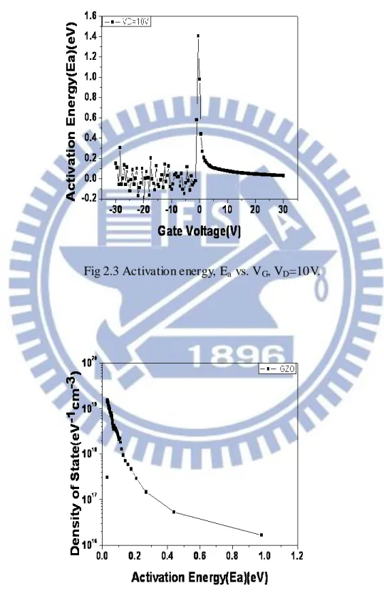
Fig 2.3 Activation energy, Ea vs. VG, VD=10V.. ………..……14
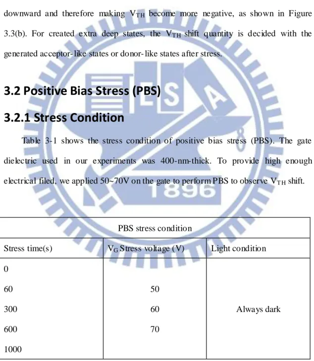
Fig 2.4 Density of states………...……….………...14
Chapter 3
Fig 3.1 The states in the band gap before bias stress...20Fig 3.2 The conceptual illustration of carriers in the band gap under positive bias stress...20
Fig 3.3(a) The conceptual illustration of carriers in the band gap under negative bias stress...21
Fig 3.3(b) The conceptual illustration of carriers in the band gap under negative bias stress and illumination...21
Fig 3.4 The PBS effects on the ID-VG curve for VG=60V...22
Fig 3.5 The VT H shift versus stress time with PBS...22
Fig 3.6 The published result of PBS with VG=60V [Ref.2]...23
Fig 3.8 The NBS effects on the ID-VG curve for VG=-60...24
Fig 3.9 The NBIS effects on the ID-VG curve for VG=-60 and illumination of 20876 Lux...24
Fig 3.10 The VT H shift versus stress time for NBS and NBIS...25
Fig 3.11 The published result of NBS with VG=-60V [Ref.2]...25
Fig 3.12 The published result of NBIS with VG=-60V [Ref.2]...26
Fig 3.13 The published results of VT H shift versus stress time for NBIS in different temperatures. [Ref.2] ...26
Fig 3.14 The DOS curve of PBS...27
Fig 3.15 The DOS curve of NBS...27
Chapter 4
Fig 4.1(a) The ID-VG transfer characteristics of a-IGZO TFTs with S/D metal of Ti/Al/Ti and their correspondent cross-section schematics...33Fig 4.1(b) The ID-VG transfer characteristics of a-IGZO TFTs with S/D metal of Cu/Ti and their correspondent cross-section schematics...33
Fig 4.2(a) The parasitic resistance extracted from a-IGZO TFTs of Cu/Ti S/D with different channel lengths...34
Fig 4.2(b) The parasitic resistance extracted from a-IGZO TFTs of Ti/Al/Ti S/D with different channel lengths...34
Fig 4.3(a) The SIMS result of the channel region for the device using Cu/Ti as the S/D metal...35
Fig 4.3(b) SIMS result of SiO2/Cu/Ti/IGZO stacked film with no pattern...35
Fig 4.4(a) The ID-VG transfer curves of a-IGZO TFT with Ti/Al/Ti S/D metal dipped in CuSO4 solution for different dipping times...36
Fig 4.5 The ID-VG transfer curves of a-IGZO TFT with Ti/Al/Ti S/D metal dipped in
di water...37 Fig 4.6 The SIMS result of the device after dipping into CuSO4 solution...37
Fig 4.7(a) The VT H shift versus stress time with Cu-dipped for 4 minutes and non-
dipped...38 Fig 4.7(b) The S.S versus stress time with Cu-dipped for 4minutes and non-dipped..38 Fig 4.8 The DOS of the devices with different dipping time...39 Fig 4.9 Schematic electronic structure of a-IGZO (DOS, density of states)...39 Fig 4.10(a) The structure and IGZO regions of the device...40 Fig 4.10(b) The DOS of region B used in the ATLAS simulation for the different
times of CuSO4 dipping...40
Fig 4.11(a) The ATLAS simulation results for the cases of acceptor- like subgap states in IGZO along with the measurement results shown in Fig. 4.4(a)...41 Fig 4.11(b) The ATLAS simulation results for the cases of donor- like subgap states in
Chapter1
Introduction
1.1 Overview and Background
With the growing need for large area displays for home entertainment and the full adoption of digital broadcasting, the active matrix flat panel display industry experienced a strong growth during the past few years. For a low mobility semiconductor like a-Si:H, designing a TFT with a large W/L ratio to achieve a high gain is necessary. Therefore, for a definite gate length, adopting TFT with higher mobility is one possible solution to achieve a smaller pixel area without sacrificing the active pixel sensing (APS) performance. It is clear that a new high mobility semiconductor material yet with a uniform amorphous phase over a large area is highly desired.
Since 2004, there has been great interest in adapting TFT made of ionic amorphous oxide semiconductors (IAOS). Specifically, the ternary oxide system which consists of In2O3, Ga2O3 and ZnO has shown promising electrical performance
for TFT active layer with a high μeff (3~12 cm2/Vs), low off current ID (<10-12A) and
expected good uniformity compatible with the state-of-the-art substrate size.
Table 1.1 compares amorphous In-Ga-Zn-O (a-IGZO) with other TFT technologies. It can be easily seen that a-IGZO TFT is currently the technology which can achieve a desired balance between high mobility and large area uniformity. Although poly-crystalline silicon (poly-Si) TFT has μeff close to 100 cm2/Vs, it
required additional re-crystallization steps such as excimer-laser annealing, metal seeding or solid phase crystallization. These add more complexity and costs to the
process. Also the substrate area used by poly-Si TFT technology is about 4 generations behind what a-Si:H TFT can achieve today. Mono-oxide semiconductor, ZnO, has been used as the active-layer in TFT channel. ZnO layer can be deposited by pulse laser deposition, RF magnetron sputtering or atomic layer de-position and the TFT μeff is around 20~50 cm2/Vs. Despite its high mobility, due to its strong
poly-crystalline nature even when deposited at room temperature, the grain boundary of such oxide semiconductor could affect device electrical properties, uniformity and stability over a large area.
Unlike ZnO, a-IGZO can have a uniform amorphous phase because multiple oxides (In2O3& Ga2O3) are introduced to promote the glass phase formation and the
amorphous phase is thermally stable up to ~500˚C. Several methods have been reported for a-IGZO deposition, including PLD, RF and DC magnetron sputtering while the latter is the most attractive due to high rate depos ition in comparison to other methods. Because of the unique electronic structure, a-IGZO is insensitive to bond angle variance of metal-oxide- metal chemical bonds induced by structural randomness. As illustrated in Fig 1.1(a), in conventional covalent bond semi- conductors (such as Si), electrons are conducting through a highly directional sp3 bonding. When these semiconductors are in amorphous state, distortions can occur in sp3 bonding and will result in reduced carrier mobility. On the other hand, in IAO S (such as In-Ga-Zn-O), electrons are conducting through metal ion’s ns orbital. Since ns orbital is symmetrical, the conducting path and carrier mobility can still be preserved even in amorphous phase (Fig 1.1(b)). To ensure a high mobility in amorphous phase, a sufficient ns orbital overlap between metal ions is necessary. To satisfy this requirement, Hosonoet al.(ref. 2) proposed a working hypothesis which predicts the metal ion should be heavy post transition metal cations with electronic configuration of (n-1)d10ns0, where n≧5. For example, the Hall mobility of the
In-Ga-Zn-O system is primarily determined by the fraction of In2O3 content in
agreement with the Hosono working theory since In3+ has the largest ionic radius (n=5) among the metal cations.
For TFT to have a low off current ID and high on-to-off ratio, it is important to
control the semiconductor carrier concentration to a very low level. In IAOS, carrier generation can occur via oxygen vacancy formation. For examples, ZnO has been reported to have a very high carrier concentration in the as-deposited states. It is usually because of the un-optimized deposition condition and the generation of excess oxygen vacancies in the thin- film. The incorporation of Ga3+ actually helps in suppressing the oxygen vacancies in a-IGZO thin- film since it has a stronger bonding to oxygen than Zn or In ions. A comparative study between a-IZO and a-IGZO has also shown that a-IGZO is able to have five orders of magnitude larger reduction in carrier concentration than a-IZO when two thin- films are deposited under the same condition.
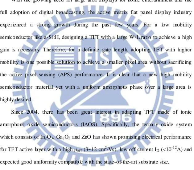
Finally, even though a-Si:H is widely used in TFT backplane, it absorbs visible photons and has a low visible light transmittance (<30%). This has been a major drawback for utilizing such material in optoelectronics and can even raise the concern of light induced instability. On the other hand, similar to ZnO, a-IGZO has a wide band-gap (~3eV) and is highly transparent in visible light (with transmittance over 90% as illustrated in Fig 1.2). This property opens up to new application such as transparent electronics or see-through display. In addition, light may directly transmit through a-IGZO TFT. This capability can permit the display or sensor to operate in the direct transmission mode for improving pixel aperture ratio.
In conclusion, a-IGZO TFTs possesses unique physical properties and better electrical performance over traditional a-Si:H TFTs.
Technology Mobility (cm2/Vs) Visible Light Transparency Large Area Uniformity Comments
a-Si:H <1 Poor Good Low mobility, limited current driving capability Poly-Si ~100 Poor Poor Additional crystallization
process required ZnO 20~50 Good Poor Strong tendency to form
poly phase
a-IGZO 3~12 Good Good Balance between mobility and uniformity Table 1.1 Comparison of different TFT technologies.
1.2 Motivation
In order to solve the internal problem of RC delay for large area display, we try to reduce the resistance of the signal buses in the TFT LCDs. Using Cu to replace Al as electrode can reduce the resistance loading in the signal metal bus effectively. Furthermore, in back channel etched (BCE) structure, although Al can be etched by wet etching on TFTs, the channel IGZO would also be etched. On the other hand, Cu can be etched by wet etching on TFTs but do not influence IGZO. There are many attempts have been made to incorporate Cu into the amorphous silicon TFT array fabrication. The process implementation of using Cu as the source/drain (S/D) metal of a-IGZO TFT is also an interesting topic to study. However, most of the previous papers about a-IGZO TFT with the application of Cu emphasized on the contact resistance and the quality of the surface between Cu and a-IGZO. In the present work,
the influence of Cu diffusion to the electrical properties of a-IGZO TFT is observed and studied.
1.3 Thesis Organization
In chapter 2, the experimental parameters and device process is described. In chapter 3, the main purpose is to check the experimental devices performance in order to make sure our devices are good and therefore the a-IGZO TFTs bias stress induced instability is investigated. In chapter 4, we introduce Cu into a-IGZO TFTs to see the induced instability, explore the instable reason and the role of Cu. In chapter 5,finally, the conclusion of the experiment and future work are given.
The section organization of this thesis is listed below:
Chapter 1: Introduction
1.1 Overview and Background
1.2 Motivation
1.3 Thesis Organization
Chapter 2: Experimental Parameters and Process
2.1 Procedures of Fabricating a-IGZO TFTs
2.2 Extraction of Device Electrical Parameters
2.2.1 Determination of the Threshold Voltage (V
TH)
2.2.2 Determination of the Sub-threshold Swing (SS.)
2.2.3 Determination of the Parasitic Contact Resistance
2.2.4 Determination of the Density of States (DOS)
3.1 Bias Stress Mechanism
3.2 Positive Bias Stress (PBS)
3.2.1 Stress Condition
3.2.2 PBS Results
3.3 Negative Bias Stress(NBS) and Negative Bias Illumination
Stress(NBIS)
3.3.1 Stress Condition
3.3.2 NBS and NBIS Results
3.4 DOS Change after Bias Stress
Chapter 4: Copper Induced Instability
4.1 Ti/Al/Ti vs. Cu/Ti Comparison
4.2 Ti/Al/Ti+CuSO
4Solution Dipping
4.3 DOS Discussion
Chapter 5: Conclusions and Future Work
Fig1.1(a) Schematic orbital drawing of electron conducting pathway (conduction band bottom) in conventional covalent bond semiconductors (e.g. Si).
Fig1.1(b) Schematic orbital drawing of electron conducting pathway (conduction band bottom) in ionic oxide semiconductors.
Fig 1.2 Absorption spectrum of the a-IGZO thin film transistor.
Chapter2
Experimental Parameters and Process
2.1 Procedures of Fabricating a-IGZO TFTs
The experimental work was based on the bottom-gate TFT devices of BCE structure with symmetrical source/drain (S/D) fabricated on the glass substrate. Shaped Ti/Al/Ti (50/200/50 nm) gate electrodes were capped with 400-nm-thick SiNx gate dielectric, which was deposited by plasma enhanced chemical vapor deposition (PECVD) at 370℃. The active layer of 60-nm-thick a-IGZO film was deposited by DC magnetron sputtering system using a target of In:Ga:Zn = 1:1:1 in atomic ratio with the O2/Ar ratio about 6%. For the S/D metals, both samples of Ti/Al/Ti
(50/200/50 nm) and Cu/Ti (200/50 nm) were prepared by DC sputtering at room temperature. Then, the devices are capped with passivation at 280℃ as protection layer to avoid the disturbance of outside surrounding. After that, via holes and ITO were patterned and shaped for device measurement. The final annealing step was conducted at 280℃ for 1 hour in the oven.
2.2 Extraction of Device Electrical Parameters
The methods of the typical electrical parameter extraction will be introduced in the following contents, including threshold voltage, sub-threshold swing (SS), parasitic contact resistance and density of states (DOS). In this study, all the electrical characteristics are measured by Agilent 4156-C system at 25℃ in dark under 1 atmosphere pressure.
2.2.1 Determination of the Threshold Voltage (V
TH)
The method to determine the threshold voltage in this thesis is the constant drain current method, which is adopted in most studies of TFTs. The threshold voltage is defined as the gate voltage which yields a normalized drain current (i.e. the threshold current). For the TFTs used in this thesis, the threshold current of 10-9 A in linear region measurement (VDS=1V) and 10-8 A in saturation region measurement
(VD S=10V) were chosen.
2.2.2 Determination of the Sub-threshold Swing (SS)
Sub-threshold swing is a measure of the efficacy of the gate potential to modulate drain current. It is defined as the amount of gate voltage to increase and/or decrease drain current by one order of magnitude. It can be shown that the expression for SS is given by
Clearly, the smaller value of SS., the better transistor is as a switch. A small value of SS. means that a small change in the input bias can modulate the output current considerably.
2.2.3 Determination of the Parasitic Contact Resistance
The purpose for extracting parasitic contact resistance is to check whether the devices’ performance variation is owing to the quality of the S/D contact. The
parasitic contact resistance can be extracted by measuring the TFTs with different channel length. With the measurement of ID-VG curve at VDS =0.1V, the total ON
resistance of TFT (RT OTAL) is represented as Eq. (1):
…………..Eq. (1)
Where rch is the channel resistance per unit channel length, R0denote the source and
drain resistance. With the use of intrinsic mobility field-effect mobility μI, the gate
insulator unit capacitor COX, and the threshold voltage VT H, rch can be represented as
Eq. (2):
………..…Eq. (2)
By substituting Eq. (2) into Eq. (1), the extractio n result of TFTs with Ti/Al/Ti and Cu/Ti as S/D metal would be informed, respectively.
2.2.4 Determination of the Density of States (DOS)
The way to extract the density of states (DOS) can follow the reference paper [ref 1]. The procedure of extracting DOS is as follows:
Step 1: To measure the ID-VG curve at different temperatures from 25℃ to 105℃
for every 20℃.
Step 2: To extract the activation energy (Ea) by plotting ln(ID) versus 1/T and
for the same VG……….Eq. (3)
Step 3: To calculate the DOS for all the Ea value by Eq. (4).
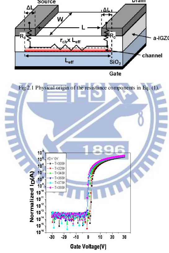
Fig 2.1 Physical origin of the resistance components in Eq. (1).
Fig 2.3 Activation energy, Ea vs. VG, VD=10V.
Chapter 3
Bias Stress Induced Instability
The Ti/Al/Ti electrodes of a-IGZO TFTs would be used on dipping into CuSO4
solution in chapter 4 to compare the influence of copper. Therefore, the main purpose for this chapter is to check the experimental device performance to make sure our devices are not unusual. Moreover, the bias stress induced instability was observed in this chapter.
In the experiments, the HP4200 precise semiconductor parameter analyzer were used to perform the stress measurement on the TFTs and to extract the transfer characteristics after stress. We used a fresh TFT sample for each stress condition to ensure the uniformity of initial characteristics and measured the transfer curves at drain to source voltage (VD S) of 1V and 10V to get the characteristics in linear region
and saturation region.
3.1 Bias Stress Mechanism
Figure 3.1 shows the band gap curve. The region that upper Fermi level is called acceptor- like states and the region the under Fermi level is called donor- like states. If we stress the device, the extra deep states will be created in a-IGZO after bias stress. The stress positive bias on gate electrode would make band bending and then electrons will be attracted in interface between nitride and a-IGZO. When Fermi level bend to upper, it will need extra electrons to fill acceptor- like states and then make VT H become higher, as shown in Figure 3.2.
should be holes attracted on interface, as shown in Figure 3.3(a). Nevertheless, it is said that there is no hole in a-IGZO because the Zn based material is reported to have large amount of states to trap holes, making holes hard to be mobilized and then become free carrier. Consequently, the VT H would have almost no shift. However, if
the device is stressed under illumination, the electron- hole pairs would be generated. These generated holes will be used to fill donor- like states when Fermi level bend downward and therefore making VT H become more negative, as shown in Figure
3.3(b). For created extra deep states, the VT H shift quantity is decided with the
generated acceptor- like states or donor- like states after stress.
3.2 Positive Bias Stress (PBS)
3.2.1 Stress Condition
Table 3-1 shows the stress condition of positive bias stress (PBS). The gate dielectric used in our experiments was 400-nm-thick. To provide high enough electrical filed, we applied 50~70V on the gate to perform PBS to observe VT H shift.
PBS stress condition
Stress time(s) VG Stress voltage (V) Light condition
0 60 300 600 1000 50 60 70 Always dark
3.2.2 PBS Results
Figure 3.4 shows the measurement result as a function of applied stress time for a-IGZO TFTs with dark stress condition at VG=60 V. The transfer curves are shifted
in the positive direction by incrementing the positive gate bias stress time but with no definite change in SS. In addition, the linear slope of the ID-VG curves does not
change much despite the increase of the positive gate bias stress time, which indicates that the change of mobility can be ignored. As a result, only the VT H shift versus stress
time is discussed here. Figure 3.5 shows the extracted result with different stressed voltages. The result shows that the VT H shift would be larger either with higher stress
voltage or longer stress time.
Furthermore, our PBS measurement results were compared with reference paper [Ref.2] whose stress condition was very similar to ours, as shown in Figure 3.6 and Figure 3.7. Both experimental PBS results of the reference paper and ours have the same behavior qualitatively. Our devices with little PBS induced instability are even better the referred ones. We now have confidence to use our device in the experiments of Cu effects.
3.3 Negative Bias Stress (NBS) and Negative Bias
Illumination Stress (NBIS)
3.3.1 Stress Condition
Table 3-2 shows the stress condition of NBS. Here we perform the negative bias stress in dark (NBS) and illuminated (NBIS) environments.
NBS stress condition
Stress time (s) VG Stress voltage (V) Light condition (lux)
0 60 300 600 1000 -60V 0 (NBS) 20876 (NBIS)
Table 3-2 Experiment conditions of DC stress.
3.3.2 NBS and NBIS Results
Figure 3.8 shows the measurement result as a function of applied stress time for a-IGZO TFTs with dark stress condition of VG=-60 V (NBS). The transfer curves
have almost no shift with stress time. As for the NBIS, the ID-VG curve is shown in
Figure 3.9, while Figure 3.10 shows the VT H shift versus stress time for both NBS and
NBIS. Obviously, the illumination effect for NBS is significant.
These results were also compared with reference paper [Ref.2], whose stress condition was very similar to ours. Figure 3.11 and Figure 3.12 show the published results of NBS and NBIS in the paper of [Ref.2], respectively. Figure 3.13 further shows effect of the bias voltage under illumination in different temperatures. Comparing to our experimental result of the VT H shift in NBIS, as shown in Figure
3.13, our devices also have better reliability. We now can say that the Cu effects to be discussed in Chapter 4 do not come from the deficiency of our devices.
3.4 DOS Change after Bias Stress
In addition to the basic ID-VG characteristics, DOS are further extracted as a
reference for the study in the Cu effects later in Chapter 4. Figure 3.14 shows the DOS curve with different positive bias stress voltages. The increase of DOS with bias voltage is attributed to the electrons attracted from the film of a-IGZO to the interface. On the other hand, Figure 3.15 shows the DOS curve with negative bias stress voltage. After NBS, electrons in a-IGZO would be expelled from the interface, resulting in the DOS decrease.
Fig. 3-1 The states in the band gap before bias stress
Fig. 3-2 The conceptual illustration of carriers in the band gap under positive bias stress.
Fig. 3-3(a) The conceptual illustration of carriers in the band gap under negative bias stress.
Fig. 3-3(b) The conceptual illustration of carriers in the band gap under negative bias stress and illumination.
Fig. 3-4The PBS effects on the ID-VG curve for VG=60V.
Fig. 3-6The published result of PBS with VG=60V [Ref.
Fig. 3-8The NBS effects on the ID-VG curve for VG=-60.
Fig. 3-9 The NBIS effects on the ID-VG curve for VG=-60 and illumination of 20876
Fig. 3-10 The VT H shift versus stress time for NBS and NBIS.
Fig. 3-12 The published result of N BIS with VG=-60V [Ref.2].
Fig. 3-13 The published results of VT H shift versus stress time for NBIS in different
Fig. 3-14The DOS curve of PBS.
Chapter 4
Copper Induced Instability
4.1 Ti/Al/Ti vs. Cu/Ti Comparison
Figure 4.1(a) and Figure 4.1(b) s show the electrical characteristics of a-IGZO TFTs with S/D metal of Ti/Al/Ti and Cu/Ti with their cross-section schematics in the insets, respectively. The average values of the VT H, μ and SS. for the Ti/Al/Ti samples
at distant sites on the glass substrate are -0.78 V, 10.13 cm2/Vs, and 0.48 V/dec, accordingly, while those for the Cu/Ti samples are 5.27 V, 8.12 cm2/Vs, and 1.58 V/dec, correspondingly. The performance of the devices fabricated with Cu/Ti S/D metal is apparently worse than that of Ti/Al/Ti samples. Because the devices processes were almost the same except for the S/D, Cu should be the factor affecting ID-VG; therefore, in order to know what happened in the device the internal
mechanisms are discussed.
The parasitic contact resistances for these devices are extracted to check whether the deterioration is owing to the quality of the S/D contact. By using the extraction method mentioned before, the extraction result of a-IGZO TFTs with Ti/Al/Ti and Cu/Ti as S/D metal are 3.15KΩ and 3.19KΩ, respectively. The extraction result excludes the possible reason that it is the quality of the metal contact to influence the device characteristics. Therefore, the factor that affects t he device transfer curve should be in the region of device channel.
Because of the high diffusivity, Cu can deeply incorporate with the IGZO film. We then come to the hypothesis that Cu in the device channel region is the reason of the deterioration in the characteristics of a-IGZO TFTs. Secondary ion mass
spectrometry (SIMS) is applied to trace the existence of Cu in depth in the channel region for the TFTs with Cu/Ti S/D, as shown in Fig 4.3(a). The profile of Cu signal distributing from the passivation to the gate insulator proves the existence of Cu.
In order to check whether Cu can penetrate through Ti or not, stacked films of IGZO, Ti, Cu, SiOx deposited on glass was also analyzed by SIMS. As shown in Figure 4.3(b), the signal of Cu is untraceable. It reveals that Cu of S/D in the contact region can hardly degrade the IGZO film with Ti as buffer metal between active layer and S/D metal.
4.2 Ti/Al/Ti+CuSO
4Solution Dipping
To further examine the Cu diffusion, non-passivated a-IGZO TFTs with S/D metal of Ti/Al/Ti were dipped into the CuSO4 solution. After the dipping process,
these devices were annealed at 280oC to imitate the deposition environment of passivation. The ID-VG curves of the a-IGZO TFTs without Cu in the S/D metal
dipped in the CuSO4 solution of the same concentration (0.05M) for various dipping
time are shown in Fig. 4.4(a), while those of the devices dipped in the CuSO4 solution
of the same dipping time (3min) for various concentration are shown in Fig. 4.4(b). The deterioration of the ID-VG curve becomes more and more serious with the
increasing dipping time or the dipping concentration.
Moreover, in order to ensure that the deterioration of the ID-VG curve comes from
the Cu ion, the influence of hydrogen should also be checked. As a result, a-IGZO TFTs were dipped in DI water and then were annealed at 280oCto study the effect of hydrogen. The result is shown in Fig 4.5. It shows that the performance of TFTs would have no change after dipping in DI water. Consequently, hydrogen should not influence TFTs performance in our experiments.
Afterwards, the SIMS result of the device with S/D metal of Ti/Al/Ti dipped into the CuSO4 solution is shown in Fig 4.6. It indicates the existence of Cu, even though
the SIMS signal is not very strong. Therefore, we conclude that the a-IGZO TFT is quite sensitive to the existence of Cu in the channel.
In addition, the bias stress induced instability of Cu-dipped a-IGZO TFTs were also compared with the non-dipped ones. Fig 4.7(a) shows the result of VT H shift
versus stress time with Cu-dipped for 4or 0 minutes. Fig 4.7(b) shows the result of SS versus stress time for the same devices. The result implies that after dipped into CuSO4 solution, not only the ID-VG curve became more and more serious but also the
bias stress induced instability became more and more instable.
4.3 DOS Discussion
In the previous report, the Cu element has been regarded as an acceptor in ZnO. The formation mechanism of wide band gap p-type conduction oxide is proposed based on the concept that the chemical bonds of Cu–O form a covalent hybridized band between the O 2p6 and Cu 3d orbitals at the top of the valence band. For a p-type oxide semiconductor, the TFT is turned on when it is biased at negative voltage. In other words, if it is the case, a significant hole current should be observed for the TFTs with negative VG. However, as shown in Fig. 4.1, the leakage current in
the devices fabricated with Cu/Ti as S/D metal is almost the same as that of conventional device. It depicts that the role of Cu can be different and needs to be discussed in more detail.
Fig. 4.8 shows the DOS of the Cu-dipped devices extracted through the measurement of ID-VG under different temperatures. The magnitude of DOS increases
from 1016 cm-3 to 1018 cm-3 with respect to the dipping time. We come to a hypothesis that the role of Cu in IGZO is more like being a defect diffusing among the atoms
than an acceptor taking the substitutive sites to provide hole.
Besides, a point of view depicts that in the TFTs there are two states called shallow states and deep states separately and the main reason influencing n-type TFTs performance is decided by shallow states. From previous report, we know that the defect states for the upper Fermi level is called acceptor- like states (also called shallow states) and the ones below Fermi level are called donor- like states (also called deep states).As a result, we further assume Cu plays the role of acceptor-like states in IGZO.
A commercial ATLAS device simulator produced by Silvaco, Inc., was used to study the possible defects that Cu can form in a-IGZO TFT. Several parameterized components were used to express the subgap density of states (DOS), such as the acceptor- like exponential and Gaussian functions and the donor- like exponential and Gaussian functions. In this work, we introduce an exponential function gexp(E)
expressed by:
to describe the DOS near the conduction band, where NT A is the conduction band
edge intercept energy, E is the state energy, EC is the conduction band edge, and WT A
is the characteristic decay energy of the exponential distribution. The subgap DOS function gG(E) that Cu forms in a-IGZO film is modeled by:
where NGA and NGD are the densities at the peak of Gaussian distribution, EGA and
EGD are the centers of the distribution, WGA and WGD are the characteristic decay
energies of Gaussian distribution for the acceptor- like and donor-like states, respectively. Since the diffusion of Cu is from the back channel of device, the defect density in the active layer near the back channel surface (region B) is set to be larger than those in the region near the front gate (region A) and the S/D contact regions (region C and D) in our simulation, as shown in Fig 4.9(a). The DOS of region B used in the simulation for the different times of CuSO4 dipping are shown in Fig. 4.9(b). The subgap states of acceptor- like and donor- like are both simulated.
Fig. 4.10(a) shows the simulation results with the increasing of acceptor-like Gaussian distribution subgap DOS and the measurement data of the CuSO4-dipping
experiment shown in Fig. 4.4(a). The simulation results fairly fit the measured curves. However, the results by increasing of donor-like Gaussian distribution subgap DOS in the same manner do not match the measurement data, as shown in Fig. 4.10(b). These simulation results suggest that the role of Cu in a-IGZO film to be an accepter-like defect near conduction band, which is consistent with the paper. The proposed role of Cu is further supported by two arguments. Firstly, according to the percolation conduction model, the worse sub-threshold swing and larger VT H indicate the increase
of deep states. In addition, Cu distributed in the a-IGZO film may act as acceptor-like trap states in the cases of silicon devices.
Fig 4.1(a) The ID-VG transfer characteristics of a-IGZO TFTs with S/D metal of
Ti/Al/Ti and their correspondent cross-section schematics
Fig 4.1(b) The ID-VG transfer characteristics of a-IGZO TFTs with S/D metal of Cu/Ti
Fig 4.2(a) The parasitic resistance extracted from a-IGZO TFTs of Cu/Ti S/D with different channel lengths
Fig 4.2(b) The parasitic resistance extracted from a-IGZO TFTs of Ti/Al/Ti S/D with different channel lengths.
Fig 4.3(a) The SIMS result of the channel region for the device using Cu/Ti as the S/D metal.
Fig 4.4(a) The ID-VG transfer curves of a-IGZO TFT with Ti/Al/Ti S/D metal dipped
in CuSO4 solution for different dipping times
Fig 4.4(b) The ID-VG transfer curves of a-IGZO TFT with Ti/Al/Ti S/D metal dipped
-30 -20 -10 0 10 20 30 10-16 10-15 10-14 10-13 10-12 10-11 10-10 10-9 10-8 10-7 10-6 10-5 10-4 N o rm a li z e d I D (A ) Gate Voltage(V) VD=10V(Initial) VD=10V(Water-dipped)
Fig 4.5 The ID-VG transfer curves of a-IGZO TFT with Ti/Al/Ti S/D metal dipped in
di water.
Fig 4.7(a) The VT H shift versus stress time with Cu-dipped for 4 minutes and
non-dipped.
Fig 4.7(b) The S.S versus stress time with Cu-dipped for 4minutes and non-dipped.
0.0 0.2 0.4 0.6 0.8 1.0 1.2 1.4 1.6 1016 1017 1018 1019 1020 D e n s it y o f S ta te ( e V -1 cm -3 )
Activation Energy (eV) initial
Cu-dipped 3 min Cu-dipped 4 min Cu-dipped 5 min
Fig 4.8 The DOS of the devices with different dipping time.
Fig 4.10(a) The structure and IGZO regions of the de vice 3.2 3.0 2.8 2.6 2.4 2.2 2.0 1.8 1.6 1014 1016 1018 1020 1022 D e n s it y o F S ta te s ( eV -1 cm -3 ) EC-E (eV) Initial Cu-dipped 3 min Cu-dipped 4 min Cu-dipped 5 min
Fig 4.10(b) The DOS of region B used in the ATLAS simulation for the different times of CuSO4 dipping
Fig 4.11(a) The ATLAS simulation results for the cases of acceptor- like subgap states in IGZO along with the measurement results shown in Fig. 4.4(a)
Fig 4.11(b) The ATLAS simulation results for the cases of donor- like subgap states in IGZO along with the measurement results shown in Fig. 4.4(a)
Chapter 5
Conclusions and Future Work
In summary, the performances of a-IGZO TFTs with and without Cu in the S/D electrodes are compared. The application of Cu/Ti as the S/D metal of the a-IGZO TFTs does not affect the parasitic contact resistance. Instead, the existence of Cu in the channel is verified by SIMS analysis and is realized to be the reason that deteriorated the ID-VG curves. The defects that form by Cu diffusion in IGZO film are
proposed to be the acceptor- like trap states below the conduction band, which explains the increased DOS and the unchanged leakage current of the TFT. The results of the CuSO4-dipping experiment are consistent with the proposed mechanism.
Considering the impact of Cu to the electrical properties of a-IGZO TFTs is so tremendous, the fabrication process of device with Cu electrode should be designed carefully.
In the future, the main target is to reduce Cu effect so that it can be applied in TFT as S/D. Therefore, what materials can reduce Cu effect should be studied. So far some materials with high dielectric constant are proposed to prevent the de leterious Cu effect. The materials are to be tested in the process of TFTs in the future.
References
[ 1 ] T. Globus, H. C. Slade, M. Shur, and M. Hack, “Density of deep
bandgap states in amorphous silicon from the temperature dependen
ce of thin film transistor current “, Mat. Res. Soc. Symp. Proc. vol. 336, 1994.[ 2 ] T.C. Chen, T.C. Chang, T.Y. Hsieh, C.T. Tsai, S.C. Chen, C.S. Lin, F.Y. Jian, and M.Y. Tsai,
“
Investigation of the gate-bias induced instability for InGaZnO TFTs under dark and light illumination“,
Thin Solid Films, vol. 520, pp. 1422-1426, 2011. [ 3 ] N. L. Dehuff, E. S. Kettenring, D. Hong, H. Q. Chiang, J. F. Wager, R. L.Hoffman, C.H. Park, and D. A. Keszler, “Transparent thin-film transistors with zinc indium oxide channel layer”, J. Appl. Phys., vol. 97, issue 6, p. 064505, 2005. [ 4 ] H.Q. Chiang, J.F. Wager, R.L. Hoffman, J. Jeong, and D.A. Keszler, “High mobility transparent thin- film transistors with amorphous zinc tin oxide channel layer ”, Appl. Phys. Lett., vol. 86, issue 1, p. 013503, 2005.
[ 5 ] M. Fryer, E. C. Colgan, E. Galligan, W. Graham, R. Horton, L. Jenkins, R. John, Y. Kuo,K. Latzko, F. Libsch, A. Lien, R. Nywening, R. Polastre, M.E. Rothwell, J. Wilson, R.Wisnieff, and S. Wright, “Planarized copper gate hydrogenated
amorphous-silicon thin- film transistors for AM-LCDs”, Mat. Res. Soc. Symp. Proc. 37, 1998, 508.
[ 6 ] P.M. Fryer, E.C. Colgan, E. Galligan, W. Graham, R. Horton, D. Hunt, K. Latzko, R Nywening, L. Jenkins, R. John, P. Koke, Y. Kuo, F. Lib sch, A. Lien, I. Lovas, R. Polastre, M.E. Rothwell, J. Souk, J. Wilson, R. Wisnieff, and S. Wright, “A six-mask TFT-LCD process using copper-cate metallurgy,” SID 96 Digest, 1996, 333. [ 7 ] H. Sirringhaus, S. D. Theiss, A. Kahn, and S. Wagner, “ Self- Passivated Copper Gates for Amorphous Silicon Thin-Film Transistors ”, IEEE Electron Device Lett., vol. 18, issue 8, pp. 388–390, Mar. 1997.
[ 8 ] H. H. Hsieh, and C. C. Wu, “Amorphous ZnO transparent thin-film transistors fabricated by fully lithographic and etching processes”, Appl. Phys. Lett., vol. 91, issue 1, p. 013502, 2007.
[ 9 ] K. Nomura, H. Ohta, A. Takagi, T. Kamiya, M. Hirano, and H. Hosono, “Room-temperature fabrication of transparent flexible thin-film transistors using amorphous oxide semiconductors”, Nature, vol. 432, p. 488, Nov. 2004.
[ 10 ] E. Fortunato, P. Barquinha, A. Pimentel, L. Pereira, G. Gonçalves, and R. Martins, “Amorphous IZO TTFTs with saturation mobilities exceeding 100 cm2/Vs”,
Phys. Stat. Sol., vol. 1, issue 1, pp. R34-R36, 2007.
[ 11 ] W. S. Kim, Y. K. Moon, S. Lee, B. W. Kang, T. S. Kwon, K.T. Kim, J. W. Park, “Copper source/drain electrode contact resistance effects in amorphous
indium–gallium–zinc-oxide thin film transistors”, Phys. Status Solidi RRL 3, No. 7–8, 239–241, 2009.
[ 12 ] J. S. Park, T. S. Kim, K. S. Son, E. Lee, K. H. Lee, W. L. Maeng, H. S. Kim, E. S. Kim, K. B. Park, J. Y. Kwon, M. K. Ryu, and S. Y. Lee, “Ti/Cu bilayer electrodes for SiNx-passivated In-Zn-O transistors: Device performance and Contact Resistance” Appl. Phys. Lett. 97, 162105, 2010.
[ 13 ] J. Kanicki, F. R. Libsch, J. Griffith, and R. Polastre, “Performance of thin hydrogenated amorphous silicon thin‐film transistors”, J. Appl Phys., vol. 69, issue 4, p. 2339,1991.12
[ 14 ] S. Luan, and G. W. Neudeck, “An experimental study of the source/drain parasitic resistance effects in amorphous silicon thin film transistors”, J. Appl. Phys., vol. 72, issue 2, p. 766, 1992.
[ 15 ] J. Jeong, Y. Hong, J. K. Jeong, J.-S. Park, and Y.-G. Mo, “MOSFET- Like Behavior of a-InGaZnO Thin-Film Transistors With Plasma-Exposed Source–Drain Bulk Region”, J. Display Technology, vol. 5, issue 12, pp. 495-500, 2009.
[ 16 ] S.-K. Rha, W.-J.Lee, S.-Y.Lee, Y.-S.Hwang, Y.-J.Lee, D.-I.Kim, D.-W.Kim, S.-S.Chun, and C.-O. Park, “Improved TiN film as a diffusion barrier between copper and silicon”, Thin Solid Films, vol. 320, pp. 134-140, 1998.
[ 17 ] T. Kamiya, K. Nomura, and H. Hosono, "Origins of High Mobility and Low Operation Voltage of Amorphous Oxide TFTs: Electronic Structure, Electron Transport, Defects and Doping", J. Display Technol. Vol. 5, issue 12, pp. 468-483, 2009.
[ 18 ] Y. Kanai, “Admittance spectroscopy of Cu-doped ZnO”, J. Appl. Phys., vol, 30, No. 4, April, pp. 703-707, 1991.
[ 19 ] M. Kim, J. H. Jeong, H. J. Lee, T. K. Ahn, H. S. Shin, J. S. Park, J. K. Jeong, Y. G. MO, and H. D. Kim, Appl. Phys. Lett., 90, 21211, 2007
[ 20 ] S. IL Kim, J. S. Park, C. J. Kim, J. C. Park, I. Song, Y. S. Parka, “High Reliable and Manufacturable Gallium Indium Zinc Oxide Thin-Film Transistors Using the Double Layers as an Active Layer”, JECS. 156 _3_ H184-H187, 2009.
[ 21 ] S. Y. Lee, D. H. Kim, E. Chong, Y. W. Jeon, D. H. Kim, “Effect of c hannel thickness on density of states in amorphous InGaZnO thin film transistor”, Appl. Phys. Lett., vol. 98, p. 122105, 2011
[ 22 ] T. Globus, H. C. Slade, M. Shour, and M. Hack, “Density of deep bandgap states in amorphous silicon from the temperature dependence of thin- film transistor current” , Materials Research Society, Mat. Res. Soc. Symp. Proc. Vol. 336, 1994 [ 23 ] K. Ueda, H. Hiramatsu, T. Kamiya, and H. Hosono, “Wide-gap layered oxychalcogenide semiconductors: Materials, electronicstructures and optoelectronic properties”, Thin Solid Films, 496, 8, 2006
[ 24 ] H.-H. Hsieh, T. Kamiya, K. Nomura, H. Hosono, and C.-C. Wu, “Modeling of amorphous InGaZnO4 thin film transistors and their subgap density of states”, Appl.
[ 25 ] A. A. Istratov, C. Flink, H. Hieslmair, E. R. Weber, and T. Heiser, “Intrinsic Diffusion Coefficient of Interstitial Copper in Silicon”, Phys. Rev. Lett., vol. 81, issue 6, pp. 1243-1246, 1998
[ 26 ] R. N. Hall and J.H. Racette, “Diffusion and Solubility of Copper in Extrinsic and Intrinsic Germanium, Silicon, and Gallium Arsenide”, J. Appl. Phys., vol. 35, issue 2, pp. 379-397, 1964
[ 27 ] N. Toyama, “Copper impurity levels in silicon”, Solid State Electronics, vol. 26, issue 1, pp. 37-46, 1983
[ 28 ]T. Kamiya and H. Hosono, “Material characteristics and applicat - ions of transparent amorphous oxide semiconductors “, NPG ASIA MATERIALS Vol. 2 January 2010


![TraditionalMLCalgorithmsmainlytacklethebatchMLCproblem,wheretheinputdataarepresentedinabatch[24,28].Nevertheless,inmanyMLCapplicationssuchase-mailcategorization[22],multi-labelexamplesarriveasastream.Onlineanalysisistherefore dimensionreducermotivatedbyma](data:image/gif;base64,R0lGODlhAQABAIAAAP///wAAACH5BAEAAAAALAAAAAABAAEAAAICRAEAOw==)