Design of A Reconfigurable Floating-Point Unit
Yun-Lung Lee, and Jer Min Jou
Department of Electrical Engineering, National Cheng Kung University
Tainan, Taiwan, R.O.C.
Email: Prof. Jer Min Jou (
周哲民
), [email protected]
Abstract
-In this paper, we propose areconfigurable floating-point unit architecture that has higher performance and flexible than the traditional integer and floating-point arithmetic unit. It can perform 8-bit, 16-bit, 24-bit and 32-bit
signed/unsigned integer multiplication, and
perform 8-bit, 16-bit, 32-bit and 64-bit add/sub adder. For floating-point operations, it can
perform IEEE standard single precision
floating-point add/sub/mul operations. For integer operations, we use “single instruction multiple data” (SIMD) technology to perform a lot of lower bit width of operands at the same operation. The proposed reconfigurable arithmetic unit can be used as a co-processing unit or an arithmetic unit in general-propose processors. The experimental result indicated that the maximum operation frequency of proposed reconfigurable arithmetic unit is 309MHz.
Keywords: Reconfigurable, Floating-point, SIMD
1. Introduction
The reconfigurable systems have both benefits of ASIC and general-purpose processor. With a reconfigurable system, we can overcome this
traditional trade-off and achieve both the
performance of ASICs and the flexibility of general-purpose processor [1].
In digital signal processing, computer graphics,
mathematical model simulation, and image
processing applications, floating-point operations is inevitable. Integer is not easy to represent fractional values, and have a limited dynamic range. For floating point arithmetic, it provides an approximation to real arithmetic that overcomes these two limitations.
But non-numerical applications usually have very few floating-point operations. In this situation, floating-point unit is always under idle mode. In idle mode, the floating-point unit still consume power and the die area is wasted. So we design a
reconfigurable floating-point unit that provide integer and floating-point operations [2].
In the recent years, multimedia applications may include video and audio that require to process different operand word lengths. Typically the video and graphics processing use 8-bit data formats. 16-bit data format is used for audio
applications and keep full precision when
processing 8-bit data. In our design, we provide various operand word lengths to support different applications for integer operations .
For floating-point operations, we design
floating-point addition, subtraction, and
multiplication in reconfigurable floating-point unit. All floating-point operations is followed by IEEE
standard single precision floating-point. The
proposed architecture is a pipeline design. The floating-point addition/subtraction has 10 pipeline cycles, and the floating-point multiplication has 12 pipeline cycles. Because of multiple pipelines the maximum operation frequency is up to 309MHz.
For integer operations, we use single instruction multiple data” (SIMD) technology to perform lots of lower bit width of operands at the same operation [3].
This paper is organized as follows. After
describing the proposed reconfigurable
floating-point unit in section 2, we will describe the design concept of an 8-bit additive multiply
module (AMM). Then we describe our
reconfigurable AMM array in section 4. Section 5 shows the experimental results and finally a conclusion with future work is given in section 6.
2. Proposed Reconfigurable Floating
Point Unit
In this section, we show the reconfigurable
floating-point unit. In order to reconfigure
floating-point unit, we use reconfigurable additive multiply module (rAMM) array (described in section 4) to provide integer operations. Because floating-point unit needs various additions and multiplication, we provide these operations by
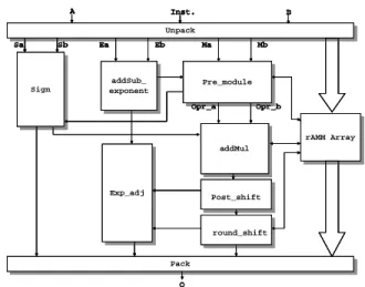
rAMM array. Figure 1 shows the reconfigurable floating-point unit. This unit consists of unpack
block, sign block, addSub_exponent block,
pre_module block, addMul block, post_shift block, round_shift block, exp_adj block, pack block, and rAMM array. The unpack block separates the integer or floating-point operands, and decodes Inst. signals. The sign block is used to determine the final sign bit. In addSub_exponent block, it
adds two exponents for floating-point
multiplication, and subtracts two exponents for floating-point addition. The pre_module is used to align two significands for floating-point addition, and bypass for floating-point multiplication. In this block, it needs 24-bit subtraction to identify which significand is larger when two exponents have same value. So we use 32-bit subtraction in rAMM array to provide this operation.
In addMul block, it performs 27-bit
addition/subtraction or 24-bit multiplication. We also use 32-bit addition/subtraction and 24-bit multiplication in rAMM array to provide these operations. In post_shift block, Zero Leading Counter (ZLC) and barrel shift are need to normalize the significand.
Because round-to-nearest-even is the default rounding scheme of the IEEE floating-point
standard [5], we use round-to-nearest-even
rounding scheme in round_shift block. It needs a 24-bit addition to perform rounding. We also use 32-bit addition in rAMM array to provide this operation. The exp_adj block is used to adjust
exponent value. In pack block, it pack
floating-point and integer into output O.
Because reconfigurable floating-point unit can provide integer and floating-point operations, the input A and B is 256-bit width which is wider than IEEE standard single precise floating-point needs 32-bit width. And output O also is 256-bit width.
The floating-point addition/subtraction has 10
pipeline cycles, and the floating-point
multiplication has 12 pipeline cycles. The integer operations have various pipeline cycles, and will describe in section 4.
2.1. The Field of Instruction Word
The instruction (Inst.) word controls the
operation of reconfigurable floating-point unit and configuration of interconnection network. The Inst. word is 6-bit and the fields of the Inst. word are shown in figure 2.
Bit 5 and Bit 4 is used to switch integer and floating-point mode. From Bit 3 to Bit 0 is used to switch integer operations.
O Unpack Unpack Sign Sign Sa Sb addSub_ exponent addSub_ exponent Ea Eb Pre_module Pre_module Ma Mb addMul addMul Opr_a Opr_b Post_shift round_shift Exp_adj Exp_adj Pack Pack rAMM Array rAMM Array A Inst. B O Unpack Unpack Sign Sign Sa Sb addSub_ exponent addSub_ exponent Ea Eb Pre_module Pre_module Ma Mb addMul addMul Opr_a Opr_b Post_shift round_shift Exp_adj Exp_adj Pack Pack rAMM Array rAMM Array A Inst. B O Unpack Unpack Sign Sign Sa Sb addSub_ exponent addSub_ exponent Ea Eb Pre_module Pre_module Ma Mb addMul addMul Opr_a Opr_b Post_shift round_shift Exp_adj Exp_adj Pack Pack rAMM Array rAMM Array A Inst. B
Fig. 1 The Reconfigurable Floating-Point Unit
1 32-bit Mul 1 24-bit Mul 4 16-bit Mul 16 8-bit Mul&MAC Multiplier Mode 4 64-bit Add/Sub 8 32-bit Add/Sub 16 16-bit Add/Sub 32 8-bit Add/Sub Adder Mode Inst. Word
Bit 3 : 0/1 => Adder / Multiplier Bit 2 : 0/1 => For Adder: Add/Sub,
For Multiplier : Unsigned/Signed Bit 1 & Bit 0 : Function definition :
11 10 01 00 11 10 01 00 0 1 2 3 4 5 4 3 2 1 0 5
Bit 5 & Bit 4 : Integer/Floating-point
00 => Integer Mode 10 => Floating Point Sub 01 => Floating Point Add 11 => Floating Point Mul
Fig. 2 The Fields of Instruction Word
3. An 8-bit Additive Multiply Module
An 8-bit additive multiply module (AMM) is a basic component for rAMM array. The AMM can receive additional addends and add them to the product of the input multiplicand and multiplier [6]. The architecture of 8-bit AMM is shown as figure 3, including a multiple-forming circuit, a partial products reduction tree, and a redundant-to-binary converter. The multiple-forming circuit is a collection of AND gates (binary multiplier). The partial products reduction tree adds all partial
products and additional addends, and then
generates carry and sum for each bit operation in redundant form. Finally the redundant result is converted to standard binary output at the bottom. An 8-bit AMM can perform the arithmetic operation such as Sum = A x B + C + W. Here A
and B are a 8-bit multiplicand and multiplier respectively, and C and W are 8-bit addend and 16-bit addend respectively. in order to perform 8-bit multiply-accumulate (MAC) operation, we extend the bit width of W from 8 bits to 16 bits.
Multiple-forming circuits
Partial products
reduction tree
Redundant-to-binary converter
8 8A
B
16 16 8 8 8 8C W
8 16Sum
16Multiple-forming circuits
Partial products
reduction tree
Redundant-to-binary converter
8 8A
B
16 16 8 8 8 8C W
8 16Sum
16Fig. 3 The Basic Architecture of 8-bit Additive
Multiply Module
4.
Proposed
Reconfigurable
AMM
Array
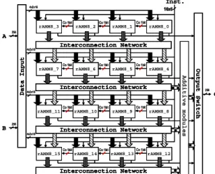
In this section, we show the reconfigurable AMM array. The reconfigurable additive multiply module array architecture is shown in figure 4. It consists of sixteen reconfigurable additive multiply modules (rAMMs), a data input, a output switch, the additive modules, and an interconnection network.
Inst.
rAMM8_3 rAMM8_2 rAMM8_1 rAMM8_0
Co 1bit Co 1bit
Co 1bit
Interconnection Network
rAMM8_7Co 1bit rAMM8_6Co 1bit rAMM8_5Co 1bit rAMM8_4
Interconnection Network
rAMM8_11 rAMM8_10 rAMM8_9 rAMM8_8
Co 1bit Co 1bit
Co 1bit
Interconnection Network
rAMM8_15Co 1bitrAMM8_14Co 1bitrAMM8_13Co 1bitrAMM8_12
Interconnection Network D a t a I n p u t A B 16x6 4x2x16 4x2x16 4x2x16 4x2x16 256 256 O u t p u t S w i t c h A d d i t i v e m o d u l e s 256 O Inst.
rAMM8_3 rAMM8_2 rAMM8_1 rAMM8_0
Co 1bit Co 1bit
Co 1bit
Interconnection Network
rAMM8_7Co 1bit rAMM8_6Co 1bit rAMM8_5Co 1bit rAMM8_4
Interconnection Network
rAMM8_11 rAMM8_10 rAMM8_9 rAMM8_8
Co 1bit Co 1bit
Co 1bit
Interconnection Network
rAMM8_15Co 1bitrAMM8_14Co 1bitrAMM8_13Co 1bitrAMM8_12
Interconnection Network D a t a I n p u t A B 16x6 4x2x16 4x2x16 4x2x16 4x2x16 256 256 O u t p u t S w i t c h A d d i t i v e m o d u l e s 256 O
rAMM8_3 rAMM8_2 rAMM8_1 rAMM8_0 rAMM8_3 rAMM8_2 rAMM8_1 rAMM8_0
Co 1bit Co 1bit
Co 1bit
Interconnection Network
rAMM8_7 rAMM8_6 rAMM8_5 rAMM8_4 rAMM8_7Co 1bit rAMM8_6Co 1bit rAMM8_5Co 1bit rAMM8_4
Interconnection Network
rAMM8_11 rAMM8_10 rAMM8_9 rAMM8_8 rAMM8_11 rAMM8_10 rAMM8_9 rAMM8_8
Co 1bit Co 1bit
Co 1bit
Interconnection Network
rAMM8_15 rAMM8_14 rAMM8_13 rAMM8_12 rAMM8_15Co 1bitrAMM8_14Co 1bitrAMM8_13Co 1bitrAMM8_12
Interconnection Network D a t a I n p u t A B 16x6 4x2x16 4x2x16 4x2x16 4x2x16 256 256 O u t p u t S w i t c h A d d i t i v e m o d u l e s 256 O
Fig. 4 The Reconfigurable AMM array
A rAMM can be configured to form a two pipeline stages 8-bit multiply-add, or one 16-bit adder or two 8-bit adders. Two rAMMs can be configured to form one 32-bit add/subtract with
two pipeline stages. Four rAMMs can be
configurable to form a five pipeline stage 16-bit multiply-adder or a four pipeline stage 64-bit adder/subtract. Nine rAMMs can be configurable to form a eight pipeline stage 24-bit multiply for floating-point multiply. The whole sixteen rAMMs can be configurable to form a 10 pipeline stage 32-bit multiply. Figure 5 shows the operations and the latency of reconfigurable AMM array can support.
The data input partitions the A and B into 16-bit for each rAMM. The additive module is used to add the higher sum and carry for multiply. Figure 6 shows the traditional 16-bit AMM multiply.
There is horizontal signal propagation in
traditional AMM multiply. That will cause
pipeline hazard (data hazard). Figure 7 shows the modified 16-bit AMM multiply. We solve the problem by adding additional additive modules.
8-bit ADD ADD
Signed 8-bit MAC (2 pipeline cycles) Unsigned 8-bit MAC (2 pipeline cycles) Signed 8-bit MUL (2 pipeline cycles) Unsigned 8-bit MUL (2 pipeline cycles) 16-bit SUB
16-bit ADD 8-bit SUB SUB
Operations 8-bit ADD ADD
Signed 8-bit MAC (2 pipeline cycles) Unsigned 8-bit MAC (2 pipeline cycles) Signed 8-bit MUL (2 pipeline cycles) Unsigned 8-bit MUL (2 pipeline cycles) 16-bit SUB
16-bit ADD 8-bit SUB SUB
Operations The operations needs 1 rAMM
32-bit ADD (2 pipeline cycles) 32-bit SUB (2 pipeline cycles)
Operations 32-bit ADD (2 pipeline cycles) 32-bit SUB (2 pipeline cycles)
Operations The operations needs 2 rAMMs
64-bit ADD (4 pipeline cycles)
Signed 16-bit MUL (5 pipeline cycles) Unsigned 16-bit MUL (5 pipeline cycles) 64-bit SUB (4 pipeline cycles)
Operations 64-bit ADD (4 pipeline cycles)
Signed 16-bit MUL (5 pipeline cycles) Unsigned 16-bit MUL (5 pipeline cycles) 64-bit SUB (4 pipeline cycles)
Operations The operations needs 4 rAMMs
Unsigned 24-bit MUL (8 pipeline cycle) Signed 24-bit MUL (8 pipeline cycle)
Operations Unsigned 24-bit MUL (8 pipeline cycle) Signed 24-bit MUL (8 pipeline cycle)
Operations The operations needs 9 rAMMs
Unsigned 32-bit MUL (10 pipeline cycle) Signed 32-bit MUL (10 pipeline cycle)
Operations Unsigned 32-bit MUL (10 pipeline cycle) Signed 32-bit MUL (10 pipeline cycle)
Operations The operations needs 16 rAMMs
Fig. 5 The operations of reconfigurable
AMM array rAMM8_0 B7~B0 A7 ~A 0 0 0 rAMM8_1 B7~B0 A1 5~ A8 0 0 rAMM8_4 B15~B8 A7 ~A 0 rAMM8_5 B15~B8 A1 5~ A8 P7~P0 P15~P8 P23~P16 P31~P24
Horizontal signal propagation
rAMM8_0 B7~B0 A7 ~A 0 0 0 rAMM8_1 B7~B0 A1 5~ A8 0 0 rAMM8_4 B15~B8 A7 ~A 0 rAMM8_5 B15~B8 A1 5~ A8 P7~P0 P15~P8 P23~P16 P31~P24
Fig. 6 The Traditional 16-bit AMM Multiply 16bit adder rAMM8_0 B7~B0 A 7~ A 0 0 0 rAMM8_1 B7~B0 A1 5~ A 8 0 0 rAMM8_4 B15~B8 A 7~ A0 rAMM8_5 B15~B8 A1 5~ A 8 P7~P0 P15~P8 P31~P16 0 Additive modules 16bit adder rAMM8_0 B7~B0 A 7~ A 0 0 0 rAMM8_1 B7~B0 A1 5~ A 8 0 0 rAMM8_4 B15~B8 A 7~ A0 rAMM8_5 B15~B8 A1 5~ A 8 P7~P0 P15~P8 P31~P16 0 Additive modules
Fig. 7 The Modified 16-bit AMM Multiply
4.1. Reconfigurable AMM Cells
Figure 8 shows the reconfigurable AMM cells
architecture. The AMM consists of
FunDecoder(Function Decoder), CSA(Carry Save Adders block), and a 16-bit rFA(Reconfigurable Fast Adders). The register support dynamic pipeline stages for different functions.
Each rAMM has five inputs from
interconnection network or data input, and three outputs are connected to interconnection network.
The multiple-forming circuit generate partial
product terms (PPts) of input A and B for multiplication. The rFA can be configured as a 16-bit adder or two 8-bit adders respectively.
Therefore, when the rAMM don’t perform
multiply operation, it can be configured to perform one 16-bit adder or two 8-bit adders. Each rAMM has unique FunDecoder. It decodes Inst. for generating control signals.
A B CSA rFA LRI TI A W Reg. 16 16 LRO TO Reg. 8(H) 8(L) 8 16 8’b0 16 8 AH BH GO PRI Reg. 16 CI CO /PRO 8 1 1 8’b0 R e g . Inst. 0 16 8 I n s t . [ 3 ] RPI_R1 sum_out sum_out_R G B C C W S1 S2 S1_R S2_R Cout Cin Sum_A Sum_B
Pipeline Register & Switch network
Pipeline Register & Switch network F u n D e c o d e r Multiple-forming Circuit A B CSA rFA LRI TI A W Reg. 16 16 LRO TO Reg. 8(H) 8(L) 8 16 8’b0 16 8 AH BH GO PRI Reg. 16 CI CO /PRO 8 1 1 8’b0 R e g . Inst. 0 16 8 I n s t . [ 3 ] RPI_R1 sum_out sum_out_R G B C C W S1 S2 S1_R S2_R Cout Cin Sum_A Sum_B
Pipeline Register & Switch network
Pipeline Register & Switch network F u n D e c o d e r Multiple-forming Circuit
Fig. 8 The Reconfigurable AMM Cells
4.2. The SIMD Design
The single instruction multiple data (SIMD)
capabilities to the multimedia applications can
provide a significant boost in performance. In our design, the rAMM array can provide SIMD
capabilities to lower bits width of integer
operations. In order to deal with lots of operands, we design 256-bit width for inputs of A and B, and 256-bit width for output of O. Table I shows the max numbers of operations at the same time.
TABLE I THEMAXNUMBERS OFOPERATIONS Multiplication Operation Max numbers Latency Unsigned/Signed 8-bit MUL&MAC 16 2 pipeline cycles Unsigned/Signed 16-bit MUL 4 5 pipeline cycles Unsigned/Signed 24-bit MUL 1 8 pipeline cycles Unsigned/Signed 32-bit MUL 1 10 pipeline cycles Addition Operation Max numbers Latency
8-bit ADD/SUB 32 1 pipeline cycle 16-bit ADD/SUB 16 1 pipeline
cycle 32-bit ADD/SUB 8 2 pipeline
cycles 64-bit ADD/SUB 4 4 pipeline
cycles
5. Experiment Results
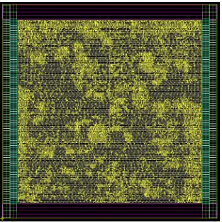
The architecture was described in Verilog HDL, and synthesized/proved within ISE 6.3i Xilinx environment, using VIRTEX II xc2v3000-4ff1152 FPGA device. Furthermore, we also synthesized, placed, and routed in TMSC 0.18nm silicon technology. Synopsys Design Compiler (DC) was used for synthesis. Synopsys Astro was used for placement and routing.
Table II show the maximum operation
frequency and area in FPGA environment and TSMC 0.18um environment. Figure 9 shows the layout of reconfigurable floating-point unit by Astro.
TABLE II
THEMAXOPERATIONSFREQUENCY ANDAREA TSMC 0.18um environment
Max frequency Area
309MHz 538062 2
um
Xilinx environment using VIRTEX II xc2c3000-4ff1152 FPGA
Max frequency Area 61.4MHz 6473 LUTs
Fig. 9 The Layout of Reconfigure Floating-Point Unit
6. Conclusion
A reconfigurable floating-point unit architecture was proposed. It can provide floating-point and
integer operations. Because the proposed
reconfigurable floating-point unit supports 21 kinds of function, the area overhead is large than a normal single precision floating-point unit. In the future, the first thing is concentrated on reducing the functions of rarely used for reducing the cost and improves a systematic design methodology for arithmetic unit with reconfigurability.
References
[1] Chien-Ming Sun, e.t. a.l., “Design of a Novel Reconfigurable Arithmetic Unit Array Architectures”, IEEE Computer Society Annual Symposium on VLSI, May 9-11,2007.
[2] Shamsiah Suhaili and Othman Sidek, “Design and Implementation of Reconfigurable ALU on FPGA”, ICECE 2004, 28-30 December 2004, Dhaka, Bangladesh.
[3] Albert Danysh and Dimitri Tan, “Architecture and Implementation of a Vector/SIMD Multiply-Accumulate Unit”, IEEE TRANS. ON
COMPUTERS, VOL. 54, NO.3, MARCH 2005.
[4] Dominique Lavenier, Yan Solihin, Kirk W. Cameron, “Integer/Floating-point Reconfigurable ALU”, Technical Report LA-UR #99-5535, Los Alamos National Laboratory, Sep 1999.
[5] Behrooz Parhami. “Computer Arithmetic Algorithms and Hardware Designs”, Oxford, 2000.
[6] Mi Lu, “Arithmetic and Logic in Computer Systems”, Wiley Interscience, 2004.