Effects of growth temperature on In N Ga N nanodots grown by metal organic chemical
vapor deposition
Wen-Hao Chang, Wen-Cheng Ke, Shu-Hung Yu, Lin Lee, Ching-Yu Chen, Wen-Che Tsai, Hsuan Lin, Wu-Ching Chou, Ming-Chih Lee, and Wei-Kuo Chen
Citation: Journal of Applied Physics 103, 104306 (2008); doi: 10.1063/1.2927249 View online: http://dx.doi.org/10.1063/1.2927249
View Table of Contents: http://scitation.aip.org/content/aip/journal/jap/103/10?ver=pdfcov Published by the AIP Publishing
Articles you may be interested in
Identification of important growth parameters for the development of high quality Al x > 0.5 Ga 1 x N grown by metal organic chemical vapor deposition
J. Vac. Sci. Technol. A 25, 441 (2007); 10.1116/1.2713409
In Ga N Ga N nanostripe grown on pattern sapphire by metal organic chemical vapor deposition Appl. Phys. Lett. 90, 013110 (2007); 10.1063/1.2430487
Structural and optical properties of In Ga N Ga N multiple quantum wells grown on nano-air-bridged GaN template
Appl. Phys. Lett. 89, 171921 (2006); 10.1063/1.2372686 In -rich In 1 x Ga x N films by metalorganic vapor phase epitaxy Appl. Phys. Lett. 85, 6131 (2004); 10.1063/1.1842375
Ga In N Ga N growth optimization for high-power green light-emitting diodes Appl. Phys. Lett. 85, 866 (2004); 10.1063/1.1779960
Effects of growth temperature on InN / GaN nanodots grown by metal
organic chemical vapor deposition
Wen-Hao Chang,a兲Wen-Cheng Ke, Shu-Hung Yu, Lin Lee, Ching-Yu Chen, Wen-Che Tsai, Hsuan Lin, Wu-Ching Chou, Ming-Chih Lee, and Wei-Kuo Chenb兲
Department of Electrophysics, National Chiao Tung University, Hsinchu 300, Taiwan
共Received 23 November 2007; accepted 18 March 2008; published online 23 May 2008兲
InN nanodots grown on GaN by metal organic chemical vapor deposition using conventional growth mode as well as flow-rate modulation epitaxy at various growth temperatures共550–730 °C兲 were investigated. We found that different precursor injection schemes together with the effect of growth temperatures greatly influenced the surface morphology of InN nanodots and their photoluminescence共PL兲 properties. The sample grown at around 650 °C showed the highest growth rate. For samples grown at higher temperatures, the residual carrier concentration was reduced and the PL efficiency was improved. Furthermore, we found that the growth of InN nanodots is still sustainable even at a temperature higher than 700 ° C while retaining their optical quality. © 2008
American Institute of Physics.关DOI:10.1063/1.2927249兴
I. INTRODUCTION
In the past few years, InN thin films with remarkably improved crystalline quality has been realized by techniques of molecular beam epitaxy1共MBE兲 as well as metal organic chemical vapor deposition 共MOCVD兲.2 Many experimental evidences have indicated that InN is a narrow-band-gap ma-terial with an energy gap near 0.69 eV,3–7 rather than the previously accepted value of ⬃1.9 eV.8 This finding has stimulated considerable interest, because the potential appli-cation of ternary InGaN alloys can be further extended into the near-infrared range. Besides the thin film growth, the fabrication of InN nanostructures, such as nanorods9,10 and nanodots,11–22 also progressed during the last few years. Such nanostructures are fascinating, since the narrow-band-gap InN combined with wide-band-narrow-band-gap barrier materials 共such as GaN or AlN兲 could form a low-dimensional system with large confinement energy. During the initial stage of heteroepitaxial growth by using either MBE共Refs.11–17兲 or
MOCVD共Refs.18–22兲, InN nanodots with controllable size
and density can be formed on GaN 共Refs. 11, 13–15, and
17–22兲 or AlN 共Refs. 17 and 19兲 templates, or directly on
Si共111兲 共Refs. 12 and 19兲 as well as nitridated sapphire16
substrates. The nucleation process, structural properties, and even strain state of InN nanodots on various substrates have recently been investigated.23,24 However, only a few reports addressed the optical properties.19–21
The growth of InN nanostructures with high crystalline quality and good optical properties for practical applications remains a great challenge. The difficulty arises not only from the large lattice mismatch between InN and the substrates, but also from the low decomposition temperature of InN.25It is expected to occur at 520– 550 ° C, resulting in a rapid escape of nitrogen atoms from the surface. If the active ni-trogen is insufficient to compensate such a decomposition,
surface accumulation of metallic indium will occur.26,27 In MBE growth of InN, this problem may be partially solved by utilizing low growth temperatures, typically below 550 ° C. However, the situation in MOCVD became even worse, due to the inefficient NH3decomposition at 600 ° C and below.25 In this regard, a higher growth temperature is preferred in the MOCVD growth of InN, in order to provide more active nitrogen. However, the growth temperature is usually limited to around 700 ° C, because of the indium desorption and other high-temperature effects, such as the increase in H2
partial pressure, which is known to significantly hinder the growth of indium-containing nitrides.28,29
In our previous works, we have demonstrated that InN nanodots with good optical quality can be prepared by the flow-rate modulation epitaxy 共FME兲.30 It is a modified growth technique of MOCVD, in which the indium and ni-trogen source precursors were alternately supplied.20,21 In this work, we further study the effects of growth temperature on the surface morphology and photoluminescence 共PL兲 properties of InN/GaN nanodots grown by FME. In addi-tions, InN dots grown by the conventional MOCVD method 共i.e., a continuous growth mode兲 have also been investigated. The different morphologies of surface dots and their depen-dences on the growth temperature and the precursor injection scheme are discussed. PL characterization was used to evalu-ate the optical properties of InN nanodots. Intrinsic proper-ties of InN nanodots, such as band gap energy, background electron concentration, and the formation of deep acceptor states, were obtained by PL line shape analysis. Our results provide valuable information for engineering the self-assembled growth of high optical quality InN nanostructures.
II. EXPERIMENTS
Samples in this study were grown on sapphire 共0001兲 substrates in a MOCVD system using trimethylgallium 共TMGa兲, trimethylindium 共TMIn兲, and ammonia 共NH3兲 as
source precursors. After nitridation of the sapphire substrate at 1120 ° C, a thin GaN nucleation layer was first grown at a兲Author to whom correspondence should be addressed. Electronic mail:
b兲Electronic mail: [email protected].
0021-8979/2008/103共10兲/104306/7/$23.00 103, 104306-1 © 2008 American Institute of Physics
520 ° C, followed by the growth of an 1-m-thick undoped GaN buffer layer at 1120 ° C. The substrate temperature was then decreased to 550– 730 ° C to grow InN nanodots. Two sets of samples with InN dots grown by FME and conven-tional MOCVD growth modes have been prepared at differ-ent growth temperatures. In FME, the gas flow sequence in one growth cycle consists of four steps: a 20 s TMIn step, a 20 s NH3 step, and two 10 s purge steps of nitrogen carrier
gas intervened in between. The TMIn and NH3 flow rates
were 150 and 18 000 SCCM共SCCM denotes cubic centime-ter per minute at STP兲, respectively. In addition, during the TMIn step, a small amount of NH3 共with a flow rate of
1000 SCCM兲 was intentionally supplied in order to suppress the reevaporation of indium atoms.21 The FME growth of InN dots were finally completed by a total of six cycles for all samples. For growing InN dots by conventional MOCVD, continuous flows of 150 SCCM TMIn and 10 000 SCCM NH3 were supplied for 120 s. Note that the total amount of
TMIn supplied in both growth methods are the same. Surface morphologies of the InN nanodots were exam-ined by atomic force microscopy 共AFM兲. PL measurements were carried out at T = 10 K in a cryostat using the 488 nm line of an argon-ion laser as an excitation source. The PL signals were analyzed by a 0.5 m monochomator and de-tected by an extended InGaAs photodiode 共with a cutoff wavelength at 2.05m兲 using the standard lock-in tech-nique.
III. RESULTS AND DISCUSSIONS A. Growth and structural properties
Surface morphologies of the InN nanodots grown at dif-ferent growth temperatures 共Tg兲 by the conventional
MOCVD and the FME methods are shown in Figs.1共a兲and
1共b兲, respectively. The scanned area for each AFM image is 10⫻10m2. It is clear that the dot size and density are
markedly influenced by the growth temperature. In general, the dot size increases whereas the dot density decreases with the increasing Tg due to the enhanced surface mobility of
adatoms. As shown in Figs.2共a兲and2共b兲the shape of these InN islands is hexagonal with a truncated flat top and steep faceted sidewalls as observed typically. The average height
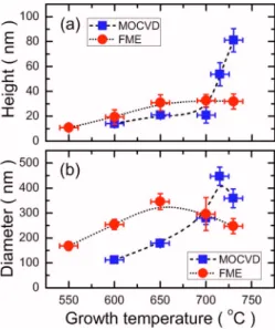
of FME dots increases from 11 to 30 nm as Tgwas increased
from 550 to 650 ° C 关see Fig. 3共a兲兴. At still higher Tg, the
average height remains constant at⬃30 nm. In contrast, the average height of MOCVD dots increases continuously even for Tg⬎700 °C, reaching 80 nm at 730 °C. Apart from the
dot height, their base length also changes with the growth temperature, as evidenced in Fig.3共b兲. It is worth to note that the aspect ratio 共height-to-diameter ratio兲 of the InN nan-odots generally increase with the increasing Tg. For MOCVD
dots, the aspect ratio is typically around ⬃1/10 for Tg
⬍700 °C and increases to ⬃1/4 at Tg= 730 ° C. On the
other hand, the FME dots are flatter than MOCVD dots, with an aspect ratio of ⬃1/16 at Tg= 550 ° C and increases to
⬃1/8 for Tg艌650 °C.
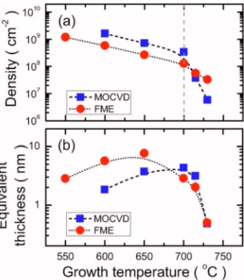
The variation of dot density as a function of Tg is
de-picted in Fig. 4共a兲. For the conventional MOCVD growth, different behaviors can be clearly distinguished at about 700 ° C. At lower growth temperatures 共Tg艋700 °C兲, the
dot density decreases gradually from 7.5⫻109to 5.0 ⫻108cm−2. However, at higher growth temperatures 共T
g
⬎700 °C兲, the dot density decreases rapidly, and eventually no InN can be grown for Tg⬎730 °C. For the case of FME,
the dot density also decreases with the increasing Tg, but
FIG. 1. 共Color online兲 AFM images of the surface morphology of InN nanodots grown at different Tg by 共a兲 FME and by 共b兲 conventional
MOCVD. The scanned area for each image is 10⫻10m2.
FIG. 2. 共Color online兲 AFM images and line profiles across typical InN nanodots grown at Tg= 650 ° C by 共a兲 conventional MOCVD and by 共b兲
FME.
FIG. 3. 共Color online兲 共a兲 The average dot height and 共b兲 diameter of the InN nanodots grown by the FME and the conventional MOCVD methods as functions of Tg.
104306-2 Chang et al. J. Appl. Phys. 103, 104306共2008兲
shows a less rapid decreasing trend at growth temperatures higher than 700 ° C, as compared with that of MOCVD samples.
Based on the surface morphology, the effective growth rate and its dependence on Tg can be estimated. This was
done by deducing the equivalent thickness of the deposited InN from the measured average height, shape, and the den-sity of these InN dots. Such results are plotted as function of
Tgin Fig.4共b兲. One can see that the highest growth rate was
achieved by the FME method at Tg= 650 ° C, corresponding
to a growth rate of⬃300 nm/h. The conventional MOCVD growth shows lower growth rates in the lower temperature range and exhibits a maximum at Tg= 700 ° C. However, the
growth rate for both methods decreases rapidly when Tg
⬎700 °C.
The InN growth is controlled by a number of factors, such as the cracking efficiency of NH3, the InN decomposi-tion, as well as the indium desorption. Because these factors are temperature dependent, the different surface dot mor-phologies and their dependence on Tg, can be understood
from the interplay among these factors together with the dif-ferent precursor injection schemes used in the FME and the conventional MOCVD methods. In general, the growth pro-cess can be divided into three regimes, distinguished by dif-ferences in the surface kinetics of indium adatoms and effec-tive In/N atomic ratio on the surface in different growth temperature ranges.
In the lower growth temperature regime共Tg⬍600 °C兲,
the growth process is mainly limited by the low cracking efficiency of NH3. The InN growth in this regime is very
inefficient so that a high NH3flow rate共or a high V/III ratio兲
is usually necessary in order to prevent the formation of in-dium droplet. Surface morphology in this regime is charac-terized by very dense islands’ nucleation, due to the low surface mobility of indium and nitrogen adatoms.
In the intermediate temperature regime 共Tg
= 600– 700 ° C兲, the InN growth proceeds from dense to sparse islands’ nucleation as Tg was increased, indicative of
an enhanced surface kinetics of adatoms. In addition, both growth methods in this regime show an increasing growth rate with the increasing Tg. This can be attributed to a higher
efficiency of NH3thermal cracking that provides more active nitrogen for the InN growth. However, the thermal decom-position of InN also becomes significant in this temperature range. Therefore, the InN growth in this regime becomes complicated by the competition between the forward and re-verse reactions, depending on the effective In/N atomic ratio on the surface. In Fig. 4共b兲, we can see that the growth rate of FME method starts to decrease when Tg⬎650 °C, which
is lower than the conventional MOCVD method occurring at 700 ° C. In FME, the InN growth proceeds only in the TMIn step, during which the background NH3 flow was kept at
only 1/10 of that used in continuous growth mode. With the increasing Tg, the small amount of background NH3becomes
unable to compensate the thermal decomposition of InN dur-ing the TMIn step, leaddur-ing to a decrease in growth rate. In addition, as can be seen from the surface morphology shown in Fig. 1共a兲, the FME samples grown at Tg⬎650 °C show
some void area共as indicated by arrow兲 that is likely to arise from the thermal decomposition of InN and subsequent re-evaporation of indium during the TMIn step. On the con-trary, thermal decomposition of InN is expected to be less significant in the conventional MOCVD growth for Tg
艋700 °C due to the continuous supply of a high NH3 flow
rate. However, it is worth to note that the growth rate of the conventional growth mode is slower than the FME method for Tg⬍700 °C. This may be a consequence of the high NH3
flow rate, leading to parasitic gas phase reactions between hydrides and indium based metal organic compounds, espe-cially when group III and group V precursors were simulta-neously injected into the reactor.
In the high-temperature regime 共Tg⬎700 °C兲, the InN
growth rate decreases rapidly, regardless of how the precur-sors were injected. Two possible effects can explain the rapid decrease in the InN growth rate. The first one is the indium desorption, which limits the sticking of indium adatoms on the growing surface and hence prevents the InN growth. Re-cently, indium desorption and InN decomposition during the MBE growth of InN have been studied in detail.26,27 How-ever, the role of indium desorption in a MOCVD reactor is still not clear, because the growth environment is much more complex than that in a MBE system. Another one is the increase of H2partial pressure produced by a more efficient NH3 thermal cracking at higher growth temperatures. It is well known that a high V/III ratio at high growth temperature will impede the growth of indium-containing nitrides, which may even lead to etching effect when a large amount of hydrogen is present.28,29Indeed, this is also the reason why it is not possible to grow InN using H2 as a carrier gas.
We also found that the use of different precursor injec-tion schemes greatly influenced the evoluinjec-tion of dot size with growth temperature. As shown in Fig. 3共a兲, the average height of FME dots tends to be saturated at Tg艌650 °C,
whereas the height of MOCVD dots increases with Tgeven
up to 730 ° C. This finding can be explained by the impact of the amount of active nitrogen on surface kinetics of indium adatoms during the nucleation of InN nanodots. In FME
FIG. 4. 共Color online兲 共a兲 The density of InN dots grown by the FME and the conventional MOCVD methods as a function of Tg.共b兲 The equivalent
thickness of the deposited InN deduced from the dot density, the average height, and the shape of the InN dots acquired from AFM measurements.
growth, InN decomposition is expected to be significant at high growth temperatures共Tg艌650 °C兲 due to the low NH3
flow rate during the TMIn step. The lack of active nitrogen might hinder excess indium adatoms from moving uphill to island tops, due to the preferential formation of In-terminated surface on the InN island tops under such In-rich conditions. As a consequence, indium adatoms tend to nucleate at the edge of InN dots, yielding islands of flat shape with a limited dot height as Tg was further increased. On the contrary,
be-cause of the high NH3 flow rate during the conventional
MOCVD growth, the exposure to a large amount of active nitrogen tends to form N-stabilized surfaces on islands tops. This facilitates uphill transfer of indium adatoms to islands tops, forming dots of significantly higher aspect ratio and hence an increasing trend in dot height even for Tg
艌730 °C.
B. Optical properties
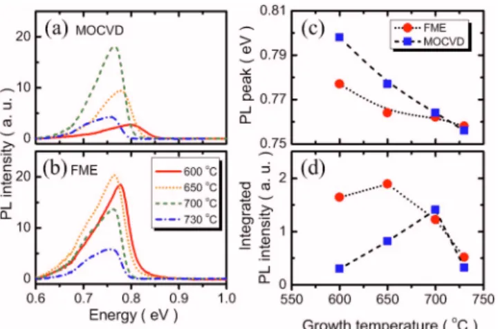
The influence of growth temperature on PL properties of InN nanodots has also been investigated. Figures 5共a兲 and
5共b兲displayed the PL spectra measured at 10 K for samples grown by FME and conventional MOCVD, respectively. No PL signal was observed for samples grown at 550 ° C. In fact, we found that InN grown at such low temperatures usu-ally shows some indium droplets on the surface due to the insufficient amount of active nitrogen. For samples grown at
Tg艌600 °C, a near-infrared PL emission band becomes
ob-servable in the range of 0.76– 0.80 eV. The corresponding peak energy共EPL兲 and integrated PL intensity 共IPL兲 as a
func-tion of Tg are plotted in Figs.5共c兲and5共d兲, respectively. A
redshift in the PL peak with the increasing Tgcan be seen for
both sets of samples. The MOCVD samples show a linear decrease in peak energy from 0.80 to 0.75 eV as Tgwas
in-creased from 600 to 730 ° C. For the FME samples, it gen-erally exhibits a lower PL peak energy than that of MOCVD samples at growth temperatures in the range of Tg
= 600– 700 ° C. As Tg⬎700 °C, similar peak energies were
observed for both sets of samples.
Due to the band filling effect of the degenerated elec-trons in the conduction band共CB兲, the PL peak energy EPLis
associated with both the band gap energy EGof InN and the
CB Fermi energy EF with respect to the bottom of CB. At
cryogenic temperatures and under low-level injections, the PL peak energy can be roughly approximated by EPL⬇EG
+ EF, as long as the Fermi level of photogenerated holes is
close to the valence band 共VB兲 edge. The electron Fermi energy EF is determined by the residual electron
concentra-tion 共ne兲 in the InN dots. On the other hand, EGmay be a
function of dot height due to the size quantization effect, especially for those dots with height⬍20 nm. Therefore, EG
should be considered as an effective energy gap, determined by both the bulk energy gap and the confinement energy of the dots. This means that both the variation in neand size
quantization of the InN dots have to be taken into account for the observed PL peak energy shift.
To distinguish the effects of size quantization and the variation in neon the PL spectra, EGand EFmust be
deter-mined separately. We have employed a line shape model to analyze our PL spectra. The line shape model considers the recombination of degenerated electrons in the CB with pho-togenerated holes bound to VB tail states and/or acceptor states.31,32The CB nonparabolicity, the energy-dependent CB density of states, as well as the corresponding electron effec-tive mass are calculated in the framework of Kane’s two-band k · p model.33 The energy parameter EP of the k · p
model was chosen to be EP= 10 eV, corresponding to an
electron effective mass of me*⬇0.065m0at the bottom of the
CB.33The electron concentration neis considered as a fitting
parameter, so that EF can be calculated from the CB
disper-sion at the Fermi wave vector kF=共32ne兲1/3. The band tail is
also determined from neby calculating the root mean square
of the fluctuated potential produced by ionized impurities.31,34In the past few years, line shape models with different levels of sophistication have been developed and utilized to analyze the PL spectra of InN.5,10,31,32,35However, because our main interest is to find EG and EF of different
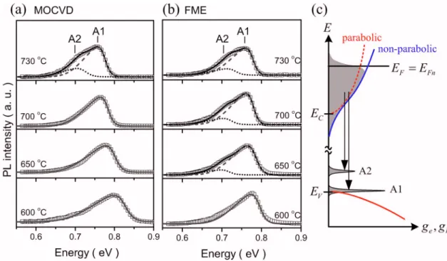
samples, the lineshape analysis was further simplified by as-suming a deltalike function for the energy distribution of photogenerated holes near the VB edge. In this way, the line shape of the PL emission band is approximated by the elec-tron energy distribution in the CB. The simulated line shapes together with the measured spectra are shown in Fig. 6共a兲
and6共b兲. The simplified model is able to give a reasonable approximation to the shape of PL spectra, especially for those MOCVD samples grown at Tg⬍700 °C. However, for
the MOCVD samples grown at Tg⬎700 °C and those FME
sample grown at Tg⬎650 °C, we found that their PL spectra
exhibit a low-energy shoulder共A2兲 at about 50–60 meV be-low the main PL peak 共A1兲, which cannot be described by the model considering only one recombination path. Accord-ing to Arnaudov et al.31 and Klochikhin et al.,32 the low-energy shoulder might be attributed to the recombination of degenerated electrons with a deeper acceptor state, as shown schematically in Fig. 6共c兲. When we included a deep accep-tor state with a binding energy of EA2= 55⫾5 meV, good
line shape fittings can be obtained.
The fitting parameters EGand neand the corresponding EFare listed in TableI, where the corresponding average dot
heights are also included for comparison. The fitted value of
FIG. 5.共Color online兲 The PL spectra of InN dots grown by 共a兲 MOCVD and共b兲 FME at various Tgfrom 600 to 730 ° C.共c兲 and 共d兲 are the PL peak
energy and the integrated PL intensity as functions of Tg, respectively.
104306-4 Chang et al. J. Appl. Phys. 103, 104306共2008兲
EG, which lies in the range of 0.688– 0.699 eV, agrees very
well with the reported values.5,10,31,32,35 It is worth to note that EF is very sensitive to the variation in ne. For the
MOCVD samples, the shift in EF is nearly⬃50 meV, even
though the variation in neis still in the same order of
mag-nitude共from 4.3⫻1018to 2.0⫻1018cm−3兲. In contrast to the
large shift in EF, the variation in EGis only about⬃10 meV.
This implies that the PL peak energy shift is mainly contrib-uted from the variation in electron concentration, whereas the size quantization effect is not significant for the investi-gated dot heights. Indeed, the fitted values of EG show a
slightly increasing trend with the decreasing height. How-ever, the variation in the effective gap cannot be attributed solely to the size quantization effect, because some other effects on bulk energy gap, such as the band-gap renormalization33 共caused by the electron-electron and electron-impurity interactions兲 and the energy position of photogenerated holes localizing in the VB tail states,31,36are also incorporated into the value of EG in the simplified
model. These effects are expected to reduce the bulk energy gap somewhat and hence counteract the size quantization effect on the fitted value of EG.
The electron concentration neobtained from line shape
fittings for both sample sets are plotted as function of Tg in
Fig.7共a兲. In both cases, the background electron concentra-tion in InN can be reduced by using a higher growth tem-perature, most likely related to a more efficient cracking of NH3. The FME samples generally show a lower ne than
those grown by MOCVD for Tg⬍700 °C, but approach
nearly the same nefor Tg⬎700 °C. Since the NH3flow rate
used in the conventional MOCVD method is considerably higher than that used during the TMIn step of FME, it can be inferred that the relatively higher nein MOCVD samples is
likely to arise from the use of a high NH3flow rate. Similar
effects have been observed in our previous study of FME grown InN dots,21 where the use of a high NH3 background flow always accompanied a high nein InN dots. Apart from
the background carrier concentration, the contribution of the deep acceptor state to the PL spectrum also depends on Tg.
As shown in Fig. 6, the low-energy shoulder appears in MOCVD samples for Tg⬎700 °C and in FME samples for Tg⬎650 °C, and becomes intense with the increasing Tg.
Interestingly, by comparing the PL spectra with the deposited
FIG. 6.共Color online兲 Line shape fitting for the PL spectra of the 共a兲 MOCVD and 共b兲 FME samples. Symbols are experimental data, while the contributions from the recombination to the VB edge state共A1 peak兲 and the deeper acceptor state 共A2 peak兲 are shown by dashed and dotted lines, respectively. The sums of the two recombination paths are indicated by the black solid curves. Gray solid curves means that only one recombination path was considered.共c兲 A schematic diagram for illustrating the recombination paths of different acceptor levels.
TABLE I. The fitting parameters共EG, ne, and EF兲 used in PL line shape fitting. The average dot heights for
different samples are also shown for comparison.
Tg 共°C兲 FME MOCVD Dot height 共nm兲 Eg 共eV兲 EF 共meV兲 ne 共⫻1018cm−3兲 Dot height 共nm兲 Eg 共eV兲 EF 共meV兲 ne 共⫻1018cm−3兲 600 19.3 0.699 94 2.6 14.5 0.697 128 4.3 650 30.8 0.695 88 2.3 20.9 0.694 105 3.1 700 32.5 0.694 83 2.1 20.8 0.694 88 2.3 730 31.8 0.693 83 2.1 81.1 0.688 81 2.0
InN amount shown in Fig. 4共b兲, one can see that the low-energy shoulder appears when the InN growth rate starts to decrease. Although we are not able to identify the species of the deep acceptor state at current stage, it is clear that the deep acceptor state originated from the high-temperature growth, most likely related to indium desorption and other high-temperature effects that hinder the incorporation of in-dium into the growing surface. Inin-dium vacancies 共VIn兲 or
their related defects arising from the lack of indium species are possible candidates for the deep acceptor state. Recently, the VIn concentration in MOCVD-grown InN film deter-mined by positron annihilation measurements was also found to increase with the increasing growth temperature.37 This experimental finding seems to support our assignment of the low-energy shoulder in PL spectra to the formation of VIn
related defects.
Regarding the PL efficiency of the InN nanodots, a high PL efficiency usually indicates a good material quality with reduced nonradiative recombination centers. In Fig.5共d兲, one can see that the integrated PL intensity as a function of Tg
shows a general correlation with the amount of deposited InN plotted in Fig. 4共b兲. In order to evaluate the PL effi-ciency of different samples, the integrated PL intensity was normalized to the amount of deposited InN, which is shown as a function of Tgin Fig.7共b兲. One can see that a higher PL
efficiency can be achieved by using a higher Tg for both
growth methods. Furthermore, with the increasing Tg, the
increase in PL efficiency is found to be larger than the de-crease in neas evidenced in Figs.7共a兲and7共b兲. For a
domi-nant Auger recombination process, the PL efficiency is ex-pected to have a 1/ne dependence. Therefore, the large
increase in PL efficiency reflects that such an improvement in PL efficiency arises not only from the reduced ne, but also
from the reduced nonradiative recombination centers. Before concluding, we would like to remark on some relevant features with regard to the growth optimization of
InN dots. In our previous work,21we have demonstrated that the size, shape, and density of the InN dots can be controlled by using different NH3 background flows in the FME
growth. In this study, as has been discussed in the Sec. III A, it is clear that the growth temperature is also an important parameter for engineering the self-assembled growth of InN nanostructures. Therefore, by optimizing both parameters, i.e., the growth temperature and the NH3flow rate, it is
pos-sible to control the size and density of the InN dots indepen-dently, in the range with surface density ranging from 6 ⫻106to 1⫻1010cm−2. In the context of realizing high
in-tensity light emitters using InN dots as an active material, the growth of small and high density InN dots is very important. In general, a higher dot density can be achieved by a lower growth temperature and a higher NH3 flow rate. However,
InN dots grown under such conditions usually show inferior optical properties. For practical applications, a compromise between the optical quality and the structural properties seems to be inevitable. Recently, Ruffenach et al.22 demon-strated that the surface density of InN dots can be further controlled by using different rare gases as a carrier gas. A very high dot density 共5⫻1010cm−2兲 was achieved by
re-placing the nitrogen carrier gas by argon. Although the influ-ence of rare gases on the optical property of InN dots is still unclear, this method may provide a different approach to achieve both high density and high optical quality InN dots.
IV. CONCLUSIONS
InN/GaN nanodots grown by the FME and conventional MOCVD methods have been investigated. The characteristic size, density, and shape of InN dots were greatly influenced by the growth temperature together with the precursor injec-tion schemes. In terms of their optical quality, the growth temperature range for InN nanodots was found to be Tg
= 600– 730 ° C. For Tg艋700 °C, higher growth rate can be
achieved at a lower growth temperature by the FME method than the conventional MOCVD growth, due possibly to the alternate injection of group III and group IV precursors, which might mitigate the parasitic gas phase reactions. The optimal growth rate was achieved by the FME method at
Tg= 650 ° C. For Tg⬎700 °C, the growth of InN by both
methods is still sustainable while retaining its optical quality, but at the expense of a very low growth rate. The effects of growth temperature on intrinsic properties of InN nanodots were studied, in which the effective band gap energy and the residual electron concentration were obtained by PL line shape analysis. We found that the incorporation of deep ac-ceptor states became more severe at a higher growth tem-perature, which might relate to the formation of In vacancies or their related defects. Our results also suggest that a higher growth temperature is beneficial for both reducing the re-sidual carrier concentration and enhancing the PL efficiency of the InN dots.
ACKNOWLEDGMENTS
This work is supported in part by the project of MOE-ATU and the National Science Council of Taiwan under Grant Nos. NSC 96-2112-M-009-006, NSC
95-2112-M-009-FIG. 7.共Color online兲 共a兲 The deduced electron concentrations nefrom line
shape model for both set of samples.共b兲 The PL efficiency as function of Tg.
The PL efficiency is obtained by normalizing the measured PL intensity to the amount of deposited InN.
104306-6 Chang et al. J. Appl. Phys. 103, 104306共2008兲
044-MY3, NSC 2112-M-009-026-MY3, and NSC 96-2112-M-009-014.
1H. Lu, W. J. Schaff, J. Hwang, H. Wu, G. Koley, and L. F. Eastman,Appl. Phys. Lett.79, 1489共2001兲.
2A. Yamamoto, T. Tanaka, K. Koide, and A. Hashimoto,Phys. Status Solidi A194, 510共2002兲.
3V. Yu. Davydov, A. A. Klochikhin, R. P. Seisyan, V. V. Emtsev, S. V.
Ivanov, F. Bechstedt, J. Furthmüller, H. Harima, A. V. Mudryi, J. Ader-hold, O. Semchinova, and J. Graul,Phys. Status Solidi B229, R1共2002兲. 4V. Yu. Davydov, A. A. Klochikhin, V. V. Emtsev, S. V. Ivanov, V. V.
Vekshin, F. Bechstedt, J. Furthmüller, H. Harima, A. V. Mudryi, A. Hash-imoto, A. Yamamoto, J. Aderhold, J. Graul, and E. E. Haller,Phys. Status Solidi B230, R4共2002兲.
5V. Yu. Davydov, A. A. Klochikhin, V. V. Emtsev, D. A. Kudrykov, S. V.
Ivanov, V. A. Vekshin, F. Bechstedt, J. Furthmüller, J. Aderhold, J. Graul, A. V. Mudryi, H. Harima, A. Hashimoto, A. Yamamoto, and E. E. Haller,
Phys. Status Solidi B234, 787共2002兲.
6J. Wu, W. Walukiewicz, K. M. Yu, J. W. Ager III, E. E. Haller, H. Lu, W.
J. Schaff, Y. Saito, and Y. Nanishi,Appl. Phys. Lett.80, 3967共2002兲. 7T. Matsuoka, H. Okamoto, M. Nakao, H. Harima, and E. Kurimoto,Appl.
Phys. Lett.81, 1246共2002兲.
8T. L. Tansley and C. P. Foley,J. Appl. Phys.59, 3941共1986兲.
9C.-H. Shen, H.-Y. Chen, H.-W. Lin, S. Gwo, A. A. Klochikhin, and V. Yu.
Davydov,Appl. Phys. Lett.88, 253104共2006兲.
10T. Stoica, R. J. Meijers, R. Calarco, T. Richter, E. Sutter, and H. Luth, Nano Lett.6, 1541共2006兲; T. Stoica, R. Meijers, R. Calarco, T. Richter,
and H. Luth,J. Cryst. Growth290, 241共2006兲.
11C. Nörenberg, R. A. Oliver, M. G. Martin, L. Allers, M. R. Castell, and G.
A. D. Briggs,Phys. Status Solidi A194, 536共2002兲.
12C. Nörenberg, M. G. Martin, R. A. Oliver, M. R. Castell, and G. A. D.
Briggs,J. Phys. D35, 615共2002兲.
13Y. F. Ng, Y. G. Cao, M. H. Xie, X. L. Wang, and S. Y. Tong,Appl. Phys. Lett.81, 3960共2002兲.
14Y. G. Cao, M. H. Xie, Y. Liu, Y. F. Ng, H. S. Wu, and S. Y. Tong,Appl. Phys. Lett.83, 5157共2003兲.
15A. Yoshikawa, N. Hashimoto, N. Kikukawa, S. B. Che, and Y. Ishitani, Appl. Phys. Lett.86, 153115共2005兲.
16Y. E. Romanyuk, R.-G. Dengel1, L. V. Stebounova, and S. R. Leone, J.
Cryst. Growth 304, 346共2007兲.
17C.-H. Shen, H.-W. Lin, H.-M. Lee, C.-L. Wu, J.-T. Hsu, and S. Gwo, Thin
Solid Films 494, 79共2006兲.
18O. Briot, B. Maleyre, and S. Ruffenach,Appl. Phys. Lett.83, 2919共2003兲.
19S. Ruffenach, B. Maleyre, O. Briot, and B. Gil, Phys. Status Solidi C 2,
826共2005兲.
20W. C. Ke, C. P. Fu, C. Y. Chen, L. Lee, C. S. Ku, W. C. Chou, W.-H.
Chang, M. C. Lee, W. K. Chen, W. J. Lin, and Y. C. Cheng,Appl. Phys. Lett.88, 191913共2006兲.
21W. C. Ke, L. Lee, C. Y. Chen, W. C. Tsai, W.-H. Chang, W. C. Chou, M.
C. Lee, W. K. Chen, W. J. Lin, and Y. C. Cheng,Appl. Phys. Lett.89,
263117共2006兲.
22S. Ruffenach, O. Briot, M. Moret, and B. Gil,Appl. Phys. Lett.90, 153102
共2007兲.
23L. Zhou, T. Xu, D. J. Smith, and T. D. Moustakas,Appl. Phys. Lett.88,
231906共2006兲.
24J. G. Lozano, A. M. Sánchez, R. García, D. González, D. Araújo, S.
Ruffenach, and O. Briot,Appl. Phys. Lett.87, 263104共2005兲.
25For a review, see, for example, A. G. Bhuiyan, A. Hashimoto, and A.
Yamamoto,J. Appl. Phys.94, 2779共2003兲.
26E. Dimakis, E. Iliopoulos, K. Tsagaraki, Th. Kehagias, Ph. Komninou, and
A. Georgakilas,J. Appl. Phys.97, 113520共2005兲.
27C. S. Gallinat, G. Koblmüller, J. S. Brown, and J. S. Speck,J. Appl. Phys. 102, 064907共2007兲.
28E. L. Piner, M. K. Behbehani, N. A. El-Masry, F. G. McIntosh, J. C.
Roberts, K. S. Boutros, and S. M. Bedair, Appl. Phys. Lett.70, 461
共1997兲.
29A. Koukitu, T. Taki, N. Takahashi, and H. Seki,J. Cryst. Growth197, 99
共1999兲.
30N. Kobayashi, T. Makimoto, and Y. Horikoshi,Jpn. J. Appl. Phys., Part 2 24, L962共1985兲; Y. Horikoshi, J. Cryst. Growth 201/202, 150 共1999兲. 31B. Arnaudov, T. Paskova, P. P. Paskov, B. Magnusson, E. Valcheva, B.
Monemar, H. Lu, W. J. Schaff, H. Amano, and I. Akasaki,Phys. Rev. B 69, 115216共2004兲.
32A. A. Klochikhin, V. Yu. Davydov, V. V. Emtsev, A. V. Sakharov, V. A.
Kapitonov, B. A. Andreev, H. Lu, and W. J. Schaff,Phys. Rev. B71,
195207共2005兲.
33J. Wu, W. Walukiewicz, W. Shan, K. M. Yu, J. W. Ager III, E. E. Haller,
H. Lu, and W. J. Schaff,Phys. Rev. B66, 201403共2002兲.
34B. I. Shklovskii and A. L. Efros, Electronic Properties of Doped
Semicon-ductors共Springer-Verlag, Berlin, 1984兲, Chap. 11.
35E. Valcheva, S. Alexandrova, S. Dimitrov, H. Lu, and W. J. Schaff,Phys. Status Solidi A203, 75共2006兲.
36B. G. Arnaudov, V. A. Vilkotskii, D. S. Domanevskii, S. K. Evtimova, and
V. D. Tkachev, Sov. Phys. Semicond. 11, 1054共1977兲.
37A. Pelli, K. Saarinen, F. Tuomisto, S. Ruffenach, and O. Briot,Appl. Phys. Lett.89, 011911共2006兲.