Integrated near-field optical head for hybrid recording
Y. Chiu*, M. Wu
a, H.P. D. Shieh
a, Y.T. Sun
b, H.L. Chou
b, W. Hsu
bDepartment of Electrical and Control Engineering, National Chiao Tung University, Taiwan, ROC
a
Institute of Electro-Optical Engineering, National Chiao Tung University, Taiwan, ROC
b
Department of Mechanical Engineering, National Chiao Tung University, Taiwan, ROC
*[email protected]; phone: 886-3-573-1838; fax: 886-3-571-5998
ABSTRACT
As the recording density of longitudinal magnetic storage increases at a 100% annual growth rate, it will soon approach the superparamagnetic limit where the thermal energy at room temperature starts to induce thermal instability to the grains in the small recorded marks. Thermal magnetic recording schemes, such as those used in magneto-optical recording, help alleviate the problems with the superparamagnetic limit. Recently, a hybrid recording system was proposed where data were recorded thermal magnetically on a magneto-optical disk and read back with a GMR head. In this paper, we propose an integrated planar head that combines an optical fiber lens, a solid immersion lens, a sub wavelength aperture, a micro coil, an air bearing surface, and a GMR head for such a hybrid recording system. Preliminary fabrication and calculation are discussed.
Keywords: near-field recording, hybrid recording, solid immersion lens, micro coil, fiber lens, sub-wavelength aperture, air bearing surfaces
1. INTRODUCTION
As the density increases and the volume of each recorded bit shrinks in advanced magnetic recording systems, a physical limit, the superparamagnetic limit [1], is quickly being approached. In this regime, the magnetic energy stored in the magnetic data bits is reduced and the thermal energy at room temperature becomes relatively significant as to induce thermal fluctuation of the recorded marks. Therefore, the anisotropic energy of the recording media must be increased in order to maintain proper thermal stability and data integrity. However, this approach will ultimately cause the media to be unrecordable with conventional inductive write heads because the required write field is too high. To overcome this problem, hybrid recording, which combines thermal magnetic recording and magneto-resistive reading, was proposed and has since attracted a lot of interest as the next generation recording technology [2]. In this hybrid recording system, the writing process is similar to the conventional magneto-optical recording, where a focused laser spot is used to heat the recording media to lower its coercivity during writing. The recording density can be increased beyond the optical diffraction limit by employing near-field recording with a solid immersion lens (SIL) or a sub-wavelength aperture. [3, 4] To read signals from such a high-density media at short sub-wavelength, a MR/GMR read head can be used to provide suitable sensitivity. Using a MR/GMR head also simplifies the optical design of the pick-up module.
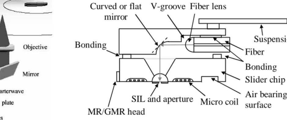
Conventional optical pick-up heads (Fig. 1) are assembled from discrete bulk optical components whose volume and weight can not be reduced easily. Hence the head modules become a limit to cost reduction and drive performance. Planar heads for near-field optical recording have been demonstrated or proposed. [5, 6] In this paper, we propose an integrated near-field head for the hybrid recording system. As shown in Fig. 2, the planar platform of this head module can be easily mounted on a suspension mechanism and fly above the spinning disk due to the aerodynamic air bearing. The module has the following components and features:
1. An optical fiber with a micro lens at the end is used to guide the light into the module. The laser diode and its related coupling optics can then be separated from the flying head to reduce its weight and volume.
2. The fiber is mounted in the V-groove on a micromachined silicon substrate. In front of the fiber lens is a curved or flat mirror surface that deflect the light vertically towards the disk.
3. In the micromachined slider chip, a SIL is fabricated on the bottom surface. A micro coil is used to provide the magnetic field for the writing process. In addition, a sub-wavelength aperture can be formed on the surface of the SIL to further reduce the spot size. Since the spot size inside the SIL is already reduced by a factor of n, where n is the refractive index of the SIL, the loss of light throughput due to the aperture is less severe compared to other near field optical probes such as tapered fibers. During the fabrication, an air bearing surface can be formed on the bottom of the slide to keep the head fly at a constant height above the disk.
4. A MR/GMR head is bonded at the trailing end of the slider to read signals from the fringing magnetic fields on the disk and perform tracking functions as in a HDD system.
2. CALCULATION
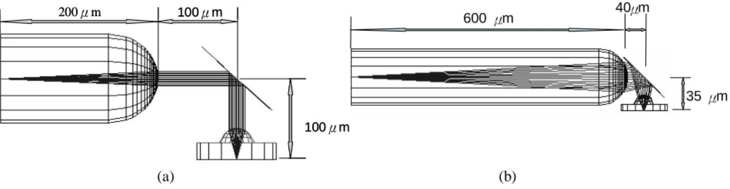
Light is guided by the optical fiber into the head module. A lens is needed to collect the diverging beam coming out of the end of the fiber. A micro lens fabricated at the end of the fiber can replace traditional bulk optical components and has the advantage of self-alignment with the fiber [7, 8]. A hemispherical micro lens with a large radius R and long working length compared to other works was designed and fabricated [9]. Optical systems with the light focused on the bottom of the SIL by various designs with such a fiberlens are shown in Fig. 3. A pure silica rod with the same refractive index as the single mode fiber core is inserted between the fiber end and the micro lens to control the focusing characteristics of the fiberlens. The equivalent NA and spherical aberration of the fiberlens-SIL assembly were calculated using ray tracing by assuming a planar wavefront on the end of the original fiber. The length of the pure silica rod g is used to control the focused beam size and its position. The relationships of effective numerical aperture (NAEFF) and Seidel coefficient (W040) as a function of rod length g are shown in Fig. 4. With small
g, the divergence of the beam inside the silica rod is small before it hits the micro lens. Therefore the NA of the fiberlens is small and it can be used as a collimating lens, as shown in Fig. 3(a). When the length of the silica rod increases, the beam diverges more inside the rod and covers more area on the micro lens. The effective NA increases and the fiberlens can be used as a focusing lens, as shown in Fig. 3(b). As can be seen from Fig. 4, both NAEFF and
aberration increase with increasing rod length. In the case of g = 0.2 mm, the incident beam from the fiber is almost collimated by the fiberlens at the cost of NAEFF reduction. On the other extreme case of g = 0.6 mm, a NAEFF of 0.7 can
be achieved with a short working distance and tight fabrication tolerance.
An aperture can be placed on the flat surface of the SIL to physically truncate the focused beam profile and further reduce the spot size. The microlens-aperture combination offers several advantages. The spot size is mainly determined by the aperture size instead of the diffraction limit. The optical throughput can be improved by several orders of magnitude over traditional tapered fibers or aperture alone. However, there is trade-off between the aperture size, and thus the spot size, and optical throughput. With the results in Fig. 4, the optical throughput, defined by the ratio of light power in the aperture to fiber illumination, for various aperture sizes is plotted in Fig. 5. Although the throughput decreases with the aperture size as expected, the value for an ~ 100 nm aperture is still high compared to conventional tapered fibers (~10-4-10-5). The throughput can be improved by optimization of the optical system design.
Fig 1. Conventional optical pickup head Fig. 2 Schematics of the proposed integrated head SIL and aperture
Bonding Bonding Curved or flat mirror V-groove Fiber Fiber lens MR/GMR head Micro coil Suspension Slider chip Air bearing surface
200Ӵm 100Ӵm
100Ӵm
200Ӵm 100Ӵm
100Ӵm
Fig. 3(a) A collimating fiberlens, and (b) a weak focusing fiberlens.
600Ӵm
35Ӵm
40Ӵm
(a) (b)
Fig. 6 Fabrication process for the fiber lens Fig. 7 Measured spot profile for λ = 0.63 µm and g ≅ 800 µm. The spot size at full width of 1/e2 is 1.00 µm and 1.02 µm in the x and y directions, respectively,
Fig. 5 Variation of optical throughput with aperture radius. ˄ˁ˘ˀ˃ˇ ˄ˁ˘ˀ˃ˆ ˄ˁ˘ˀ˃˅ ˄ˁ˘ˀ˃˄ ˄ˁ˘ʾ˃˃ ˃ ˄ˆ˃ ˅ˉ˃ ˆˌ˃ ˈ˅˃ ˉˈ˃ ˊˋ˃ ˴̃˸̇̈̅˸ʳ̆˼̍˸ʳʻ́̀ʼ ̂̃ ̇˼˶ ˴˿ ʳ̇˻ ̅̂ ̈˺ ˻̃ ̈̇ ˺ʳːʳ˃ˁˉʳ̀̀ ˺ʳːʳ˃ˁˈʳ̀̀ ˺ʳːʳ˃ˁˇʳ̀̀ ˺ʳːʳ˃ˁˆʳ̀̀ ˺ʳːʳ˃ˁ˅ʳ̀̀ Silica rod length g(mm)
NA S p h e ric a l a ber ra tion ( lan da)
Silica rod length g(mm)
NA S p h e ric a l a ber ra tion ( lan da)
Fig. 4 The relationships of effective numerical aperture (NAEFF) and Seide coefficient (W040)
as a function of the silica rod length g.
Sp h e ri c a l a b e rra ti o n ( λ ) NA
3. FABRICATION
Several components in the integrated optical head have been fabricated and characterized. 3.1 Fiber lens
The fabrication process for the hemispherical fiberlens is schematically illustrated in Fig. 6 [9]. The micro lens was formed by applying a high-frequency arc discharge to melt the fiber tip (Fig 6(b)). As discussed in the above, the silica rod length g is used to control the focusing characteristics of the fiberlens. The focused spot of the hemispherical microlens was imaged onto a vidicon tube (PST-203, Kuge Precision Co., Ltd.) by a high numerical aperture objective lens. For λ = 0.63 µm and g ≅ 800 µm, the spot size at full width of 1/e2 is 1.00 µm and 1.02 µm in the x and y directions, respectively, as shown in Fig. 7.
3.2 V-groove and 45° mirror
Wet anisotropic chemical etching can reveal well-defined crystallographic planes in silicon substrate. In particular, the KOH/water/IPA etchant can be used to fabricate structures formed by the (110) Si planes, which make an 45°angle with the surface of a (100) Si substrate, with improved surface smoothness [10, 11]. In our experiments, a 1.2- µm-thick SiO2 layer was used as the etching mask for a rectangular groove opening oriented at 45° with respect to the
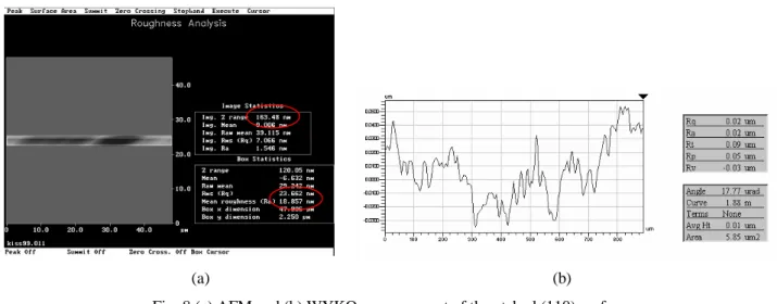
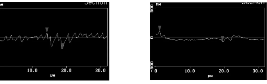
primary <110> wafer flat. The sample was etched in a saturated KOH/IPA solution under constant stirring. The roughness of the 45° mirror surfaces determines the quality of the reflected beam and focused spot. An atomic force microscope and a WYKO interferometer were used to measure the surface smoothness and roughness. Fig. 8 shows typical AFM and WYKO measurements of the mirror surfaces. The best results with surface roughness around 25 nm were obtained from an etching solution with 30 wt% KOH and 25 vol% IPA. For λ = 0.63 µm, this roughness corresponds to less than 25th of a wavelength. Another important optical property of the mirror is its smoothness, which is indicated by the Z range parameter in the AFM scan and Rt in the WYKO measurement. As indicated in Fig. 8(a) and 8(b), this parameter is in the range from 100 nm to 200 nm over the entire measured area. How this surface variation affects the beam quality also depends on the size of the beam on the mirror. If, for example, the beam diameter is about 50 µm as indicated in Fig. 3(a), the effect will be more severe for the sample in Fig. 8(a) than 8(b). Nevertheless, a novel approach was tried to improve the smoothness of the etched surfaces. After the wet etching, photoresist was coated over the 45° surfaces. Due to its fluidic nature, it is expected to smooth out the unevenness and roughness on the surfaces and improve the surface optical quality. Fig. 9 shows the AFM measurement before and after the photoresist coating. The vertical distances in the line scan were successfully reduced from 270 nm to 180 nm. Experiments are undergoing to further reduce the variation and improve the smoothness of the etched mirrors.
(a) (b)
3.3 Slider chip
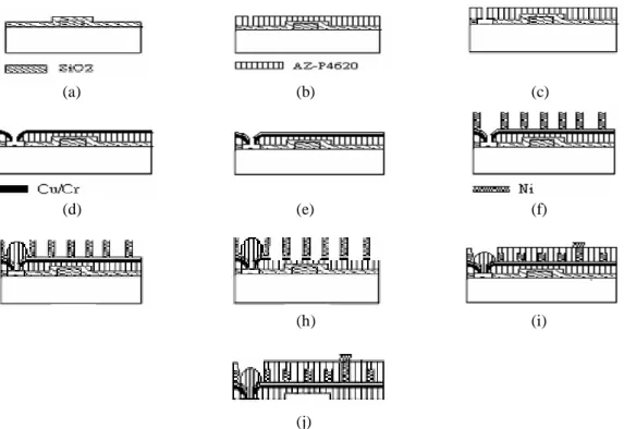
The fabrication process of the slider chip in the head module is shown in Fig. 10. Major components in this chip include an air bearing surface, an aperture, a micro coil, a solid immersion lens, and other mechanical support structure. First, a PECVD SiO2 layer was deposited and patterned to form the air-bearing structure. A second PECVD SiO2 of 6 µm thickness was then deposited as the sacrificial layer for the final release process (Fig. 10(a)). The fabrication process for the aperture is shown in Fig. 10(b) to 10(e). After the coating of 5-µm-thick AZ-P4620, an initial aperture with a diameter of 2 µm was defined (Fig. 10(b)). After the lithography process, the photoresist was reflowed at 150
°C to form a curved aperture entrance. A 1500 Å Cu/Cr layer was then sputtered as the seed layer for subsequent
copper electroplating (Fig. 10(d)). Copper overplating was used to reduce the original aperture size [12]. By controlling the time and recipe of electroplating, apertures with nanometer scale could be fabricated (Fig. 10(e)). After the aperture was fabricated, a 30-µm-thick AZ-P4620 layer was coated and patterned as the electroplating mold for the microcoil. After the microcoil was electroplated and the photoresist mold removed (Fig. 10(f)), another AZ-P4620 layer was coated and patterned to form a cylinder post at the location of the micro solid immersion lens. After a thermal reflow process, the SIL with a hemispherical shape can be obtained (Fig. 10(g)). The seed layer for the electroplating process was then removed to prevent short circuit in the micro coil (Fig. 10(h)). A last electroplating process was performed to form electrical interconnection and bonding pads (Fig. 10(i)). The finished slider chip can then be bounded with the above V-groove chip. The releasing process can be carried out by a BOE etching of the sacrificial SiO2 layer (Fig. 10(j)).
Fig. 11 shows the reduction of the aperture size by overplating. With a current density of 3 mA/cm2, the diameter was shrunk from 1.66 µm for 2 minutes of plating to 0.64 µm for 10 minutes of plating. Fig. 12 shows a reflow micro solid immersion lens with a diameter of 90 µm. The lens was made of photoresist AZ-P4620, of which the index of refraction was found to increase from 1.63 to 1.82 after the thermal reflow process. Further investigation is undergoing to understand and control the index variation with the process parameters. An integrated module with the aperture, SIL and microcoil is demonstrated in Fig. 13. The thickness of the microcoil is about 15 µm. The electroplating parameters such as current density, temperature, and solution recipe were critical to the fabrication of microcoils. Non-optimized electroplating parameters will cause large internal stress and rough surface profile. A “wetting” step is also needed to ensure good plating results. Wafer should be dipped in the D.I. water to remove the air entrapped in the structure before electroplating. Otherwise, large current density will be induced at the locations on the surface covered by residual air bubbles.
4. CONCLUSION
An integrated optical pickup head is proposed for near field hybrid recording. Optical system performance was calculated. Several components in this integrated module were fabricated and characterized. Further optimization of system design, individual component fabrication, and system integration are being pursued. This work is supported by the National Science Council of the Republic of China under Contract No. 89-E-FA06-1-4, “Photonics Science and Technology for Tera Era” Center of Excellence.
Fig. 9 AFM line scan (a) before and (b) after photoresist coating
(a) (b) (c)
(d) (e) (f)
(h) (i)
(j)
Fig. 10 Fabrication process of the slider chip: (a) air bearing surface definition by two SiO2 layers, (b)
initial aperture definition by AZ-P4620, (c) undercut etching of SiO2, (d) Cu/Cr seed layer sputtering,
(e) copper overplating, (f) micro coil electroplating, (g) SIL patterning and reflow, (h) seed layer etching, (i) interconnection electroplating, (j) BOE release
Fig. 11 Aperture size for different electroplating time, (a) 1.66 µm for 2 minutes, (b) 0.64 µm for 10 minutes
(a) (b)
Fig. 12 Reflow microlens with diameter of 90 µm. Fig. 13 Integrated module with the aperture, SIL, and microcoil.
REFERENCES
1. S.H. Charap, P.L. Lu, and Y. He, IEEE Trans. Mag., Vol. 33, pp. 978-983, 1997.
2. H. Sukeda, H. Saga, H. Nemoto, Y. Itou, C. Haginoya, and T. Matsumoto, IEEE Trans. Mag., Vol. 37, No. 4, pp. 1234-1238, 2001.
3. B.D. Terris, H.J. Mamin, D. Rugar, W.R. Studenmund, and G.S. Kino, Appl. Phys. Lett., 65(4), pp. 388-390, 1994. 4. I. Ichimura, S. Hayashi, and G.S. Kino, Appl. Opt., Vol. 36, No. 19, pp. 4339-4348, 1997.
5. K. Kato, S. Ichihara, N. Kasama, M. Oumi, T. Niwa, Y. Mitsuoka, and K. Nakajima, Technical Digest, ISOM 2000, pp. 188-189, 2000
6. K. Ueyanagi and T. Tomono, Jpn. J. Appl. Phys., Vol 39, Pt. 1, No 2B, pp. 888-891, 2000 7. L. Cohen and M. Schneider, Appl. Opt. Vol. 13, 89, 1974
8. C. Edwards, H. Presby, and C. Dragone, J. Lightwave Tech., Vol. 11, 252, 1993
9. Chung-Hao Tien, Yin-Chieh Lai, Tom D. Milster, and Han-Ping D. Shieh, Jpn. J. Appl. Phys. Vol. 41, pp.1834-1837, 2002.
10.C. Strandman, L. Rosengren, and Y. Backlund, IEEE, pp. 244-249, 1995
11.C. Strandman, L. Rosengren, Hakan G. A. Elderstig, and Y. Backlund, J. MEMS, Vol. 4, No. 4, pp. 213-219, 1995. 12.Trans Lane, Wensyang Hsu, International Symposium on Optical Memory (ISOM) 2001, pp. 252-253