國 立 交 通 大 學
電子物理研究所
碩士論文
次微米的雷射位移感測器之研究
Study of laser sensor for sub-micron displacement measurement
學生:龔家楨
指導教授:蘇冠暐 教授
Study of laser sensor for sub-micron displacement measurement
研究生:龔家楨 Student : Chia-Chen Kung
指導教授:蘇冠暐 Advisor : Kuan-Wei Su
國立交通大學
電子物理研究所
碩士論文
A Thesis Submitted to Institute of Electrophysics
College of science
National Chiao Tung University
In Partial Fulfillment of the Requirements
For the Degree of Master of Science
In Electrophysics June 2010
Hsinchu, Taiwan, Republic of China
次微米的雷射位移感測器之研究
學生:龔家楨
指導老師:蘇冠暐 教授
國立交通大學電子物理研究所碩士班
摘 要 本論文的研究目的在於根據三角測量法原理去設計一個20 kHz 高速量測且解析 度達到次微米級的雷射位移感測器,描繪出一維的物體表面形貌,以運用在工業 的產品缺陷檢測上。由探究雷射三角測量法的原理與架構來提高解析度;分析成 像透鏡產生的光學像差並使用光圈加以修正;從雷射光特性得知,藉由擴束鏡和 聚焦透鏡來獲得較小的檢測光點以提昇精確度。搭配輸出模態佳、功率可調的倍 頻綠光固態雷射以及雜訊低、靈敏度高的影像感測器組成雷射位移量測系統,對 於量測多晶矽的表面位移量,提出最佳化的質心演算法以達到次微米級解析度和 高速量測目的。Study of laser sensor for sub-micron displacement
measurement
Student : Chia Chen Kung Advisor: Prof. Kuan Wei Su
Insitute and Department of Electrophysics
National Chiao Tung University
Abstract
The purpose in this study is to design a laser triangulation displacement sensor with high speed about 20 kHz and resolution up to sub-micron class, which can be applied to inspection in the industry by describing one dimension profile. We study principle of triangulation to improve the resolution and correct the optical aberration with aperture. To use beam expander and focus lens with analysis of laser feature gets smaller spot diameter which raises precision. Diode pumping solid state laser has fine output mode and power modulation and image sensor possesses the characteristic of low noise and high sensitivity. Integrate them into displacement measurement system. For poly-silicon surface displacement, we propose optimization centroid algorithm to achieve sub-micron resolution and fast sampling speed with the measurement system.
誌 謝
兩年的碩士生活一轉眼就過去了,在這兩年我學習到很多,如今要正式邁向新的 階段,在這裡要感謝我的指導教授蘇冠暐老師在這兩年的指導,老大的實驗能力 和細心思維是我學習的對象,還有陳永富老師的教誨,讓我見識到身為一流學者 的風範,使我受益良多。另外,感謝已經畢業的學長姊-陸亭樺學姊、黃仕璋、 黃哲彥、陳建誠學長們,實驗室的成員-張漢龍、黃文政、梁興弛、依萍、雅婷、 余彥廷、陳毅帆、莊威哲、毓捷、黃郁仁、林昆毅在實驗上的幫忙與生活上的陪 件。最後我要感謝我的父母和家人以及我的朋友,有你們的支持與鼓勵,讓我充 滿能量與活力。 感謝大家!!Contents
摘要
………... IAbstract
……….………... II誌謝
.………..………...………... IIIContents
……….…..……….… IVList of Figures
…………...………... VIList of Tables
………... VIIIChapter 1 Introduction
1.1 Motivation
………..……….……... 1
1.2 Analysis and methods of displacement
…………... 21.2.1 Time of flight ……… 2
1.2.2 Interferometry……….…….. 5
1.2.3 Triangulation………..…..……… 6
1.3 Literatures review
……….…………..………... 91.4 Organization
……...………..………..……...……… 10Chapter 2 Optical configuration and principle of laser
triangulation displacement sensor
2.1 Principle of laser triangulation
……….……... 112.2 Related derivation of optical path
………..………….. 152.3 Optical aberrations
………... 202.4 Spot size and measuring rage of laser beam
……….. 27Chapter 3 Photo-electronic devices and experiment set up
3.1 Laser source
….………..………… 343.1.1 Semiconductor laser……….… 34
3.1.2 Diode Pump Solid State Laser……….… 35
3.2 Optical sensor
………... 363.2.1 Position sensitive detector……….... 37
3.2.2 CCD Image Sensor………... 38
3.2.3 CMOS image sensor………... 40
3.2.4 Comparison of CCD and CMOS image sensor……..….. 42
3.3 Test object
….………... 43
3.4 Measurement system
……….………. 46Chapter 4 Laser displacement sensor experiment result
and optimization
4.1 Optical centroid
………...………..……. 504.2 Poly-silicon surface measurement
………..…..……… 59Chapter 5 Summary and future work
….…..……….……... 64List of Figures
Fig. 1.1 Laser pulse measuring technique………….….……… 3
Fig. 1.2 Phase-shift technique……...……….………...……. 4
Fig. 1.3 Frequency-modulated continuous wave………….……….. 4
Fig. 1.4 Michelson Interferometer.……….………. 5
Fig. 1.5 Triangulation………...……….….. 6
Fig. 1.6 Relation of measuring range and spot displacement ….……….. 7
Fig. 1.7 Commercial laser displacement sensor………….……….….. 8
Fig. 1.8 Principle of confocal microscopy………... 9
Fig. 1.9 Optical triangulation patent………..……… 10
Fig. 2.1 Optical triangulation.……..…...……….…..… 12
Fig. 2.2 Image on the focal plane……….... 13
Fig. 2.3 Scheimpflug condition………..……….…… 14
Fig. 2.4 Image on focus plane of triangulation………..……….. 15
Fig. 2.5 Triangulation geometry………..…….……….…….. 16
Fig. 2.6 Magnification and position relation at m=1………..…. 18
Fig. 2.7 Different magnifications………. 19
Fig. 2.8 Wave-front aberrations………. 20
Fig. 2.9 Spherical aberration………….………. 22
Fig. 2.10 Coma………...…. 23
Fig. 2.11 Astigmatism………... 23
Fig. 2.12 Field curvature……….. 24
Fig. 2.13 Distortion………..……… 24
Fig. 2.14 Ernostar lens module…………...………. 25
Fig. 2.15 Correct coma………...………. 25
Fig. 2.16 Circle far-field diffraction……….…….………..….. 26
Fig. 2.17 Pattern for different aperture size…………..……….…………...…. 26
Fig. 2.18 Laser beam propagate in the space ………. 28
Fig. 2.19 One-dimensional distribution of light intensity at z=0………... 29
Fig. 2.20 Laser transmit through the lens………..…… 29
Fig. 2.21 Laser transmit through the beam expander……….. 32
Fig. 2.22 Laser operating distance and measuring range………..…. 33
Fig. 3.2 PSD structure……….…...…..….. 37
Fig. 3.3 PhotoMOS structure……….……… 38
Fig. 3.4 Charge transfer of CCD……….…………..………….….... 39
Fig. 3.5 Signal output circuit of CCD…..……...………..…. 39
Fig. 3.6 Three-phase clock……….…….………..………. 40
Fig. 3.7 CMOS sensor section structure………..………..………… 41
Fig. 3.8 CMOS (a)PPS(b)APS sensor …………..………..……….. 41
Fig. 3.9 Reflection situation ………..………... 43
Fig. 3.10 Lambert’s cosine law……….……….……..……… 44
Fig. 3.11 Spot Size and object surface……….……..……….. 44
Fig. 3.12 Different Spot size measure the metal plate……….……… 45
Fig. 3.13 Laser specification………..……….. 47
Fig. 3.14 Stage (Newport)………...……… 47
Fig. 3.15 CCD (YAYA Co. Ltd. offer)……….……… 47
Fig. 3.16 PCI express (EURESYS Co. Ltd.)...…………..…..………..…….. 47
Fig. 3.17 Poly-silicon measurement………..………..……… 47
Fig. 3.18 Experiment setup………...……..…….………… 49
Fig. 4.1 Displacement relation of sample and spot (I)…………..………. 51
Fig. 4.2 CCD centroid…………... 52
Fig. 4.3 Comparison between original data and centroid……….………. 53
Fig. 4.4 (a) Non-removed and (b) removed noise intensity distribution…..…. 53
Fig. 4.5 Comparison between non-removed and removed noise with centroid 54
Fig. 4.6 Displacement relation of sample and spot (II)…... 54
Fig. 4.7 Percentages of the centroid……….………..……… 57
Fig. 4.8 Intensity distribution of spot at the origin………….………..………. 58
Fig. 4.9 1-D poly-silicon displacement measurement ……….……...….……. 63
List of Tables
Tab. 2.2 Spot size of different focus lens ……….…………. 33
Tab. 4.2 Correlation coefficient of percentage intensity ………...…. 58
Tab. 4.3 Pixel numbers of intensity percentage ………...…..…….…... 59
Chapter 1 Introduction
1.1 Motivation
Measurement is objective and accurate to describe matter or phenomenon. It is one of manners that human explore the nature. The properties of light including wavelength, intensity, phase, coherent length and polarization are ways to measure range, angle and shape. The characteristic is noncontact measurement. Comparing with contact measurement system, light has no need to contact the object’s surface to avoid damaging external. Since T. H. Maiman invented the first ruby laser in 1960, electro-optical engineering have developed quickly. Laser measurement instrument has simple structure and high precision due to directionality, monochromaticity, coherence and brightness. Laser displacement sensor is important in the industry because it can achieve fast scan speed, high precision and measuring range widely. In the industrial applications are such as vibration, surface profile, flaw detection, component inspection, positioning [1]. With technology development, the dimensions of manufacture have become from micrometer, submicron until nanometer. We have to study higher precision laser displacement sensor forindustry. Purpose of thisstudy is on the basis of triangulation to design laser displacement sensor for slight displacement measurement. Integrate beam-expender, focus lens, aperture and centroid algorithm into laser displacement sensor with high precision, fast scanning speed about 20k Hz, and low cost. We expect resolution of the laser displacement sensor is 0.1 μm class.
1.2 Analysis and methods of displacement
Non-contact measurements divide into three methods based on their different theorems [2]. They are time of flight, interferometry and triangulation. Time of flight measures time by sending signal until accepting back signal. According to coherence, interference forms fringes owing to different optical length. Triangulation has triangulation geometry to calculate distance. They have different applications to measure range by different theorems.
1.2.1 Time of flight
Time of flight divides into three methods which are pulsed, phase shift and frequency modulated continuous-wave. As laser source sends pulses, counting system count numbers of clock-pulsed at the same time until acceptor receives back pulses signal. Measuring distance is τ cn ct L 2 1 2 1 = = (1.1) Where c is velocity of light, t is time of travel, n is numbers of clock-pulse, and τ is period of clock-pulse. Pulse laser which resolution is about 1 meter is suited to measure distant range. For example, to obtain 1 mm accuracy has to measure 6.7 ps interval. Moreover, different ranges are measured by different laser sources. Semiconductor laser with low power is applied to hundred meters range, and Nd-YAG laser with high power is applied to kilometers range. The laser pulse time-of-flight distance measuring technique was used in military and surveying. New applications are such as sensors in robotics and autonomous vehicles.
Fig. 1.1 Laser pulse measuring technique
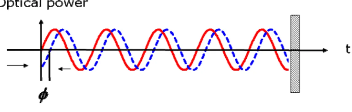
Phase shift technique is that the laser power modulated with constant frequency is a sine wave in the phase shift range finder. Phase shift after reflection from the target is
ϕ=2 f tπ (1.2) Travel time is
c 2L
t= (1.3) Phase shift can be written as
2L 2 f
c
ϕ = π (1.4) Measurement of the distance is
π φ 2 2f c L= (1.5)
Phase-shift technique which resolution is about 1 mm is suitable for shorter range. It will become 3-D vision system due for low cost in the future.
Laser source system
Counting system Accepted system
Fig. 1.2 Phase-shift technique
Frequency modulated continuous wave (FMCW) technique [3][4] is used on radar. In the same way that it can be use on laser range finder. The optical power from a frequency modulated laser diode, as triangulation wave or saw-tooth wave, is periodically shifted by fΔ .Intermediate frequency is
f cT L f T t fif = Δ = 2 Δ (1.6) Distance is if f f cT L Δ = 2 (1.7)
Fig. 1.3 Frequency-modulated continuous wave
The FMCW technique has been used in various applications such as noncontact surface profiling, fiber optic sensing, reflectometry, positioning and tomography.
t 0 f f Δ c L t = 2 f T = 1 if f Reference signal Object signal f
1.2.2Interferometry
Fig. 1.4 Michelson Interferometer
Michelson interferometer is familiar configuration. Light beam splitting into two paths produce interference fringes on detector due to different optical path.
Phase shift is d 2 2 λ π φ = (1.8) If φ is a multiple of 2π , it indicates all constructive or all deconstructive behavior.
2
λ
n
d = (n=1,2,3...) (1.9)
Its resolution is half of wavelength. However, Michelson interferometer didn’t measure absolute distance so that multi-wavelength interferometer has developed [4][5]. 2 2 2 1 1 1 2 2 π λ φ λ π φ ⎟ ⎠ ⎞ ⎜ ⎝ ⎛ + = ⎟ ⎠ ⎞ ⎜ ⎝ ⎛ + = n n L ⎟⎟ ⎠ ⎞ ⎜⎜ ⎝ ⎛ − = π φ λ 2 2 1 1 1 L n detector laser d
⎟⎟ ⎠ ⎞ ⎜⎜ ⎝ ⎛ − = π φ λ 2 2 2 2 2 L n
(
)
⎥⎦⎤ ⎢⎣ ⎡ − + − ⎟⎟ ⎠ ⎞ ⎜⎜ ⎝ ⎛ − = π φ φ λ λ λ λ 2 2 1 2 1 1 2 2 1 2 1 n n L (1.10)When Δ (φ φ2−φ1) is 2π , the distance is known by measuring fringes difference of the two wavelengths. Its resolution is
⎟⎟ ⎠ ⎞ ⎜⎜ ⎝ ⎛ − = Λ 2 1 2 1 λ λ λ λ (1.11) Interferometry is not suited to use in the industry, because it has to keep steady around when measures in spite of high precision.
1.2.3 Triangulation
Triangulation [7] is composed of light source, test object and optical sensor. The source project light beam onto the object surface, image lens collects part of the scattered light on the optical sensor. Distance of measurement is calculated by triangle geometry with light source, test object and optical sensor.
Fig. 1.5 Triangulation
L
D
x
x Df
L= (1.12)
Where D is distance of focus lens and image lens, f is focal length of image lens, x is distance of image lens and position of light spot on the photon detector, and L is distance of focus lens and target.
Fig. 1.6 Relation of measuring range and spot displacement [7]
Fig. 1.6 shows that resolution raise if x becomes lower value. Triangulation is general distance measurement due to simple structure, high accuracy and operating rage wide. Thus triangulation has applied to surface inspection in the industry [8][9].
x Df L= L δ L z δ L x δ δx L x
L
Fig. 1.7 Commercial laser displacement sensor [10]
As Fig. 1.7 shown, when shift test object position, the location of the laser spot on the detector also changes. Additionally, confocal system is one method of optical inspection, and it can restructure 3-D micro-structure. Its resolution achieves nanometer class, for example, confocal microscopy. Confocal means that point light source emits light through the lens focuses on the test object and reflects original path. Confocal microscope is that places splitter mirror to change ray path, pinhole and detector on the focus shown in Fig. 1.8. Therefore, we concluded the surface shape can measure by means of the detected intensity [11]. Confocal microscope has smaller resolution, but the detection rate is too slow, and suitable for reflective material surface. This does not agree with industry.
Fig.1.8 Principle of confocal microscopy
1.3 Literatures review
In 1969, J. R. Kerr proposed that geometric triangulation method can inspect thickness and surface morphology defect of the system in plywood manufacturing [12]. Then numbers of non-contact optical system began to develop and commercialize. In 1971, triangulation method with light sensors (PSD) and microcomputer applied in industry, and the first commercialization of the triangular sensor was developed by Diffracto Limited, Dynavision and Selcom three companies [13]. Z. JI and M.C. LEU published the design of optical triangulation to improve the measurement resolution and range in 1989 [14]. T.A. Clarke, K. T. V. Grattan analyzed the errors about triangulation including photon sensors and laser source in 1991 [15]. In addition, Rejean Baaribeau and Marc Rioux proposed the light speckle for measuring range in 1991 [16]. In 1994, Rainer G.. Dorsch, etc. investigated speckle for position uncertainty [17]. In 1997, Shao-Qing Wang proposed a new formula to fix the error for measurement using triangulation rough surface [18].
Light point
Photon detector
Fig.1.9
Optical triangulation patent
[19]1.4 Organization
Next, we illustrate the structure and basic principles of the triangulation; third is to introduce optoelectronic devices and experiment setup; the final shows the experiment result and optimization algorithm for poly-silicon.
Chapter 2 Optical configuration and principle of laser
triangulation displacement sensor
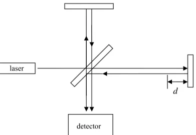
Triangulation laser displacement sensor composes of laser source, image lens and photon detector. Typical triangulation laser displacement sensor can divide into two types. One of them is based on angle altering by reflection laws, so the test object has to be specular surface. Another is by means of collecting scattering light on the optical sensor, so the test object has to be rough surface. Reflection laser displacement sensor holds higher resolution than scattering laser displacement sensor [20]. Nevertheless, common object belongs to the latter. Design laser displacement sensor for rough surface is the purpose in this article. Now keyence company product is with measuring range 2 mm and 0.01 μm.
2.1 Principle of laser triangulation [14]
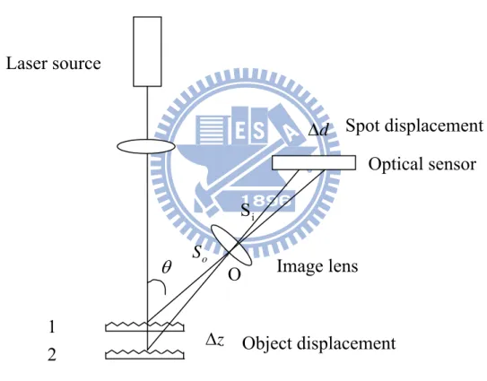
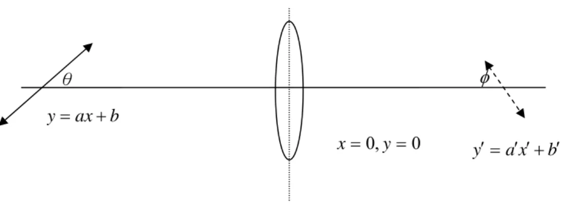
Laser triangulation is laser beam projects on test object surface, light is scattered by surface, and image lens collects scattered light on the optical sensor. Displacement relation of test object and spot are formed triangulation geometry as shown in Fig. 2.1.
Fig. 2.1 Optical triangulation
The roughness extent on test object surface is slighter than displacement for optical measurement system. Roughness is the cause of light scattering. Displacement ( zΔ ) of test object is shorter than distance (S ) between test object and image lens. The o
angle of location 1 or and lens optical axis is the same. The displacement of light spot on the photon sensor is
θ sin z m d = ×Δ Δ
With object displacement shifting, light spot can not focus on the image place. This will result in aberration so that read out the position of light spot is hard. Thus, we have to put the optical sensor on the image plane. According to Gaussian lens formula, the trace of object displacement is object plane and the location of optical sensor is on the image plane. We consider the object distance which only appears real image.
z
Δ
θ
1
2
O
Light source
Spot displacement
Object displacement
d
Δ
Optical sensor
Image lens
oS
iS
Fig. 2.2 Image on the focal plane
Gaussian lens formula
f S So i 1 1 1 + =
Fig 2.2 shows that equations represent their trace. Trace of object displacement represents y=ax+b. Where a is its slope, b is intercept (object distance) and θ
is equal totan−1a. Trace of image plane represents y′=a′x′+b′. Where a′ is its
slope, b′ is intercept (image distance) and φ is equal to tan−1a′.
Under Gaussian lens formula
f x x 1 1 1 = ′ + f x f x x − ′ ′ = (2.1) Magnification is f f x f x f x x x x m = ′− − ′ ′ ′ = ′ = (2.2)
Trace of image plane is
) ( ax b m
y′= − +
− (2.3)
y′ and a add to negative due to opposite and real image.
θ 0 , 0 = = y x b ax y= + φ b x a y′= ′ ′+ ′
(2.1) instead of (2.3), we obtain ) ( b f x f x a m y − − ′ ′ = ′ (2.4) (2.2) instead of (2.4), we obtain b x f b a y′=( − ) ′+ (2.5)
This is trace of image plane. For instance, we set that focal length of the image lens is 5 cm, θ is 45°, and b=10 cm . The previous conditions instead of Eq. (2.5) to obtain 10y′=−x′+ . This indicates a′ is -1 and φis equal to 45°.
From Eq. (2.5) we learn the image plane has relation to object distance, angle with lens axis and focal length. This is Scheimpflug condition. Suppose object plane is perpendicular to optical axis in the beginning. When object plane tilts with vertical line, image plane also tilts at the same time. Object plane, image plane and lens plane intersect a point, it is called Scheimpflug condition.
Fig. 2.3 Scheimpflug condition [21] Optical axis A B A′ B′ Object plane Image plane θ
S
s′
θ′ Lens planem is magnification,and the relation of object plane and image plane for finite angle is θ θ θ tan tan tan m s s′ = = ′ (2.6) For slight angle, it can be written
θ θ θ m s s = ′ = ′ (2.7) Fig. 2.4 shows the design of triangulation sensor has to be base on Scheimpflug condition to obtain high resolution.
Fig 2.4 Image on focus plane of triangulation
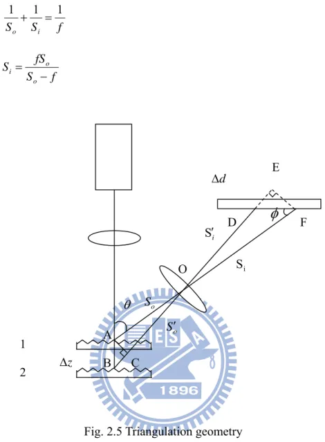
2.2 Related derivation of optical path
We know that the optical sensor has to place on the image plane location. Next, we find out the relation of displacement of object and spot on the photon sensor. As Fig. 2.5 shown, it follows Gaussian lens formula
z
Δ
θ
1
2
O
Laser source
Object displacement
d
Δ
Optical sensor
Image lens
oS
iS
Spot displacement
f S So i 1 1 1 + = f S fS S o o i = −
Fig. 2.5 Triangulation geometry
Magnification defines o i S S m=
From similar triangle ΔAOC~ΔFOE, we obtain
z AB=Δ θ sin z AC=Δ d DF =Δ φ sin d EF =Δ z Δ d Δ
φ
θ 1 2 A B C D E F O o S i S o S ′ i S′From magnification relation, we obtain θ φ sin sin z d AC EF S S m o i Δ Δ = = = (2.8) The relation of displacement of object and spot on the photon sensor is
z m d = Δ Δ φ θ sin sin (2.9) The shape of one dimensional is from
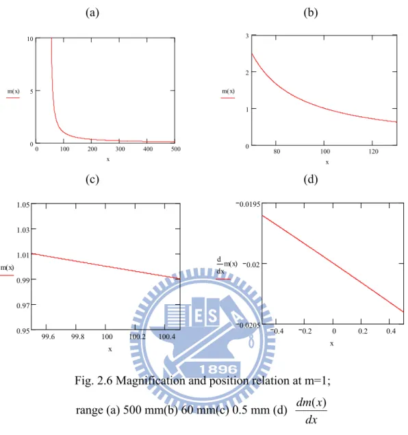
d m z= Δ Δ θ φ sin sin 1 (2.10) Displacement of spot and object are proportion to magnification. Here, the magnification is not constant value. Start afresh to find m(x) from (2.2)
f x f x f x xf x x m − = − = ′ = (2.11) Set f =50mm, Fig. 2.6 indicate relation between x and magnification equals to 1.
Magnification tends infinite when x locates focus. If x is lower, m(x) and
dx x
dm )(
also become lower. m(x) takes as constant when interval of Δx is slight.
From simplifying Eq. (2.9), We can obtain
z k
d ∝ Δ
Δ (2.12)
(a) (b) 0 100 200 300 400 500 0 5 10 m x( ) x 80 100 120 0 1 2 3 m x( ) x (c) (d) 99.6 99.8 100 100.2 100.4 0.95 0.97 0.99 1.01 1.03 1.05 m x( ) x 0.4 0.2 0 0.2 0.4 0.0205 0.02 0.0195 xm x( ) d d x
Fig. 2.6 Magnification and position relation at m=1; range (a) 500 mm(b) 60 mm(c) 0.5 mm (d)
dx x
dm )(
The angle with object displacement and image lens axis sets 45°. Fig 2.7 indicates magnifications are 0.5、1、2. The spot displacement is an upward curve because magnification is an inverse ratio with object distance which relation fit the curve from Eq. (2.9) and Eq. (2.11). Additionally, Equation (2.9) exhibits to obtain high resolution when magnification becomes larger.
(a) 114 112 110 108 106 104 102 100 98 96 94 92 90 -10 -8 -6 -4 -2 0 2 4 6 8 10 m = 1 S pot of di sp la cme nt (m m) Object of position (mm) (b) 81 80 79 78 77 76 75 74 73 72 71 70 -10 -8 -6 -4 -2 0 2 4 6 8 10 m =2 Spot of di sp la cm en t (mm) Object position (mm) (c) 180 175 170 165 160 155 150 145 140 135 130 -10 -8 -6 -4 -2 0 2 4 6 8 10 Sp ot of di sp la cm en t (m m ) Object position (mm) m=0.5
Fig. 2.7 Different
magnifications
(a)1:1(b)1:2(c)2:1 left are experiment result ;right are simulation result
-14 -12 -10 -8 -6 -4 -2 0 2 4 6 8 10 -10 -8 -6 -4 -2 0 2 4 6 8 10 Sp ot d is placem en t (m m ) Object displacement (mm) sample forward sample backward -6 -5 -4 -3 -2 -1 0 1 2 3 4 5 -10 -8 -6 -4 -2 0 2 4 6 8 10 Spot di spl ac em en t (mm) Object displacement (mm) Object forward Object backward -30 -25 -20 -15 -10 -5 0 5 10 15 20 -10 -8 -6 -4 -2 0 2 4 6 8 10 light -spot disp lacement (mm) Object displacement (mm) sample front sample back
2.3 Optical aberrations
Optical aberrations have two kinds. One is chromatic aberration for different wavelength. Another is lens aberration including spherical aberration, coma aberration, astigmatism, curvature of field and distortion. We don’t consider chromatic aberration since mono-wavelength radiating by laser source. When laser beam project on the object surface, we see the spot as new light point source. Scattered light from the point source radiates is collected by image lens focus on the photon sensor, so we must consider lens aberration effect.
Wave-front aberration means object point radiates spherical wave when pass through image lens, and then spherical wave-front distorts due to optical path different.
Fig. 2.8 Wave-front aberrations
The optical path is equal in the same wave-front, so wave-front aberration is be written
[
]
[
]
(
[
]
[ ]
)
(
[
] [ ]
)
[
OADE]
[
OADR] [ ]
RE nRE O R OADR O E E D A O O OAD O D A O W ′ = = − = ′ + − ′ + = ′ − ′ = (2.13) Define the object horizontal and vertical coordinates(ξ,η), pupil coordinates ( yx, )Ray α R: Reference circle Optical axis
A E D A D O E O′ n Chief ray n′
and wave-front function(x,y,ξ,η). θ ξ θ η η θ η θ ξ ξ θ θ θ θ sin cos sin cos sin cos sin cos ′ + ′ = ′ − ′ = ′ + ′ = ′ − ′ = x y y y x x (2.14)
The above equations satisfy invariant transformation. We only consider vertical direction that η has value and ξ is equal to zero. Express by polar coordinates
) , , , (ρ φ ξ θ W ,expand it order high W W W W W W W W W W W + + + + + + + + + + = 4 00 4 3 11 3 2 2 20 2 2 2 2 22 2 3 31 1 4 40 0 2 00 2 11 1 2 20 0 00 0 cos cos cos cos ) , , ( η φ ρ η ρ η φ ρ η φ ηρ ρ η φ ηρ ρ φ η ρ (2.15) jk
W is aberration coefficient. The location of chief ray is usually as a reference point.
There is no aberration. 0W00=2W00=4W00 =0. Simplify Eq. (2.15) to obtain
order high W W W W W W W W + + + + + + + = φ ρ η ρ η φ ρ η φ ηρ ρ φ ηρ ρ φ η ρ cos cos cos cos ) , , ( 3 11 3 2 2 20 2 2 2 2 22 2 3 31 1 4 40 0 11 1 2 20 0 (2.16) One-order aberration: 2 20 0W ρ (defocus) φ ηρcos 11 1W (tilt) Three-order aberration: 4 40 0W ρ (spherical aberration) φ ηρ3cos 31 1W (coma) φ ρ η2 2 2 22 2W cos (astigmatism) 2 2 20 2W η ρ (field curvature) φ ρ η3 cos 11 3W (distortion) (1) Spherical aberration
Parallel rays passing lens can focus on point. However, give a convex lens example. The farther position of off-axis resulting in that has more powerful to refract light. The different focus on the optical axis with distance makes blur image. Spherical aberrations divide into longitudinal spherical aberration (LSA) and lateral spherical aberration (TSA). The location
∑
LC which has clean image is called circle of least confusion.Fig. 2.9 Spherical aberration
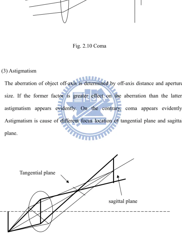
(2) Coma
The parallel light not parallel with optical axis doesn’t focus on one point after passing lens. The image looks like comet dragged. In Fig. 2.10, chief ray and marginal ray focus on the different location.
F’ LSA TS A Incident light
∑
LC F F”Fig. 2.10 Coma
(3) Astigmatism
The aberration of object off-axis is determined by off-axis distance and aperture size. If the former factor is greater effect on the aberration than the latter, astigmatism appears evidently. On the contrary, coma appears evidently. Astigmatism is cause of different focus location of tangential plane and sagittal plane.
Fig. 2.11 Astigmatism
Positive coma
Tangential plane
(4) Field curvature
The focus plane of common optical systems is spherical surface not plane surface, so we observe blur image at edge.
Fig. 2.12 Field curvature (5) Distortion
Distortion results from different distance between each point of object and lens. Pincushion distortion is lateral magnification increases gradually ; barrel distortion is lateral magnification reduces gradually.
Fig. 2.13 Distortion Focus spherical plane
Aberrations affect spot location on the optical sensor, so we must face to correct the aberrations. The solution of aberration is generally to construct compound lens. For example, Keyence Co. Ltd. produces a series of LK-G laser displacement sensor which uses Ernostar lens to correct aberration for high precision. In this study, we use aperture to achieve the target. To place the aperture forward the lens closely, it obstructs scattering light and let paraxial ray pass through center of the image lens. Correcting coma is necessary for spot location because coma is asymmetrical pattern. Moreover, aperture can control brightness and spot size.
Fig. 2.14 Ernostar lens module [22]
(a) (b)
Fig. 2.15 Correct coma
Positive coma Positive
If we narrow the aperture enough small, the image plane emerges from circle of far field diffraction. The intensity distribution is
2 1 sin ) sin ( 2 ) 0 ( ) ( ⎥⎦ ⎤ ⎢⎣ ⎡ = θ θ θ ka ka J I I ( R q = θ ) (2.17) This pattern is called Airy disk. The intensity distribution looks like Gaussian function.
Fig 2.16 Circle far-field diffraction
(a) (b)
(c) (d)
Fig. 2.17 Pattern for different aperture size (a)5 mm(b)3 mm(c)1.5 mm(d)1 mm φ ρ a Φ P 0 P q z y θ R Z Y
2.4 Spot size and measuring rage of laser beam
Spot size of the laser beam influences space resolution. If the spot size is small, it can attain more precise result. Therefore, we need to reduce the spot size of laser beam. Compositions of laser are three elements including pumping source, gain medium and resonant cavity. Pumping source offers energy for electron transition from lower level to higher level. Gain medium contains population inversion. Resonant cavity determines output mode which are two resonant modes. Longitudinal mode governs width of line spectrum; transverse mode governs diffused angle, laser spot and output power. Laser propagation behavior satisfies wave equation
0 ) , , ( ) (∇2+ 2 = z y x u k (2.18)
Here z is propagation direction. According to paraxial, the field distribution is
⎟ ⎟ ⎠ ⎞ ⎜ ⎜ ⎝ ⎛ ⎟⎟ ⎠ ⎞ ⎜⎜ ⎝ ⎛ + + − − ⎟⎟ ⎠ ⎞ ⎜⎜ ⎝ ⎛ − ⎟⎟ ⎠ ⎞ ⎜⎜ ⎝ ⎛ ⎟⎟ ⎠ ⎞ ⎜⎜ ⎝ ⎛ ⎟⎟ ⎠ ⎞ ⎜⎜ ⎝ ⎛− + = − ) tan ) 1 ( ( exp ) ( 2 exp ) ( 2 ) ( 2 ) ( ) ( exp ) ( ) , , ( 2 0 1 2 2 2 2 0 , w z n m kz i z R kr i z w y H z w x H z w y x z w w z y x umn m n π λ (2.19)
Where H is Hermitian polynomial, m and n are node numbers, w(z)is spot radius
and w is the smallest spot size. 0
For the propagation of the smallest spot radius as the beam waist, it gradually expands along the z-axis transmission
⎟ ⎟ ⎠ ⎞ ⎜ ⎜ ⎝ ⎛ ⎟⎟ ⎠ ⎞ ⎜⎜ ⎝ ⎛ + = ⎟ ⎟ ⎠ ⎞ ⎜ ⎜ ⎝ ⎛ ⎟⎟ ⎠ ⎞ ⎜⎜ ⎝ ⎛ + = 2 0 2 0 2 2 0 0 2 0 2( ) 1 1 z z w w z w z w π λ (2.20) ) (z
R is the radius of curvature of the laser related to radius.
⎟ ⎟ ⎠ ⎞ ⎜ ⎜ ⎝ ⎛ ⎟⎟ ⎠ ⎞ ⎜⎜ ⎝ ⎛ + = ⎟ ⎟ ⎠ ⎞ ⎜ ⎜ ⎝ ⎛ ⎟⎟ ⎠ ⎞ ⎜⎜ ⎝ ⎛ + = 2 0 2 0 2 0 1 1 ) ( z z z z w z z R λ π (2.21)
Defined Rayleigh range 0 2 0 0 λ πw z = (2.22)
Rayleigh range is between near field and far-field behavior of transition region. Transverse electromagnetic wave (TEM) modes represent the electric field distribution in space. TEM00 is the lowest mode called the Gaussian Beam. The solution is ⎟ ⎟ ⎠ ⎞ ⎜ ⎜ ⎝ ⎛ ⎟⎟ ⎠ ⎞ ⎜⎜ ⎝ ⎛ − − ⎟⎟ ⎠ ⎞ ⎜⎜ ⎝ ⎛ − ⎟⎟ ⎠ ⎞ ⎜⎜ ⎝ ⎛− + = − ) tan ( exp ) ( 2 exp ) ( ) ( exp ) ( ) , , ( 2 0 1 2 2 2 2 0 0 , 0 w z kz i z R kr i z w y x z w w z y x u π λ (2.23)
Fig. 2.18 Laser beam propagate in the space
Gaussian intensity distribution is
) ) ( 2 exp( ) ( 2 2 2 2 0 0 z w r z w w I I = − (r= x2 +y2) (2.24) 0 ω θ ω( )z z
Fig 2.19 One-dimensional distribution intensity at z=0 Divergence angle defines
0 0 ) (
lim
dwdzz w z π λ θ = = ∞ → (2.25) Laser spot is proportional to propagation distance, but inverse with the beam waist radius. Gaussian beam is very important in optical. Its features include beam energy transmission is limited to in cylinder, transverse spatial distribution is symmetrical circle, and spot of light intensity distribution is Gaussian function. It also more concentrates energy than high order mode, and light spot gathered into smaller enough.Fig. 2.20 Laser transmit through the lens
f z z′ o w o w′ w w′
Relative amplitude of intensity
0
ω
0.135
x or y
Thin lens curved surface is as wave front. Light upon the thin lens is the incident wave front into the output wave front, and Gaussian beam passes though thin lens is still Gaussian Beam, but phase changes. We can write down
(
)
(
)
(
)
⎟⎟ ⎠ ⎞ ⎜⎜ ⎝ ⎛ − ′ + + = + − ⎟⎟ ⎠ ⎞ ⎜⎜ ⎝ ⎛ − + + 2 0 0 2 2 2 2 2 0 0 2 2 tan ) ( 2 tan ) ( 2 w z z R y x k kz f y x k w z z R y x k kz π λ π λ (2.26) Induct to f z R z R 1 ) ( 1 ) ( 1 = − ′ (2.27) w w′= (2.28)Gaussian beam propagates z′ distance through the lens, the relation can be written
(
2)
2 0 1 R w w w ′ + = ′ λ π (2.29)(
2)
1 w R R z π λ ′ + ′ = ′ − (2.30) 2 0 0 1+⎜⎝⎛ ⎟⎠⎞ = z z w w and ⎥ ⎦ ⎤ ⎢ ⎣ ⎡ ⎟ ⎠ ⎞ ⎜ ⎝ ⎛ + = 1 0 2 z z zR substitute into Eq. (2.29) and Eq. (2.30)
to obtain
(
) ( )
2 0 0 2 0 w z f z f w + − = ′ (2.31)(
z f) ( )
z(
z f)
f f z − + − = − ′ 2 0 2 2 (2.32) 0 =z substitutes into Eq.(2.31) and Eq. (2.32) can simplify
2 0 0 0 1 ⎟ ⎠ ⎞ ⎜ ⎝ ⎛ + = ′ f z w w (2.33)
2 0 1 ⎟ ⎠ ⎞ ⎜ ⎝ ⎛ + = ′ z f f z (2.34)
If laser beam is as incident light from infinite (2z0 >> f ), simplifyEq.(2.33) and Eq.
(2.34) f f w w 0 0 0 π θ λ = ≈ ′ (2.35) f z′≈ (2.36)
We conclude focal spot is proportional to the focal length of lens and wavelength of laser, but inverse with light spot radius [23].
The waist radius of laser light is decided by the laser cavity, so we cannot change the parameters. However, we can use beam expander to change the spot diameter of incident light. 01 0 02 w f w π λ = (2.37) 01 1 2 02 w f f w = (2.38)
We obtain smaller waist radius with expander and focus lens than only with focus lens.
Fig. 2.21 Laser transmit through the beam expander
The focal depth is a problem considered in optical system. The focal depth means the rage keeps image quality despite of deviating from the focus. We define the range within 1.05w as focal depth [24]. Use Eq. (2.23) to solve measuring range 0 Δ z
λ π 2 0 32 . 0 w z =± Δ (2.39) Above the equations show the relationship is between the beam waist radius and the focal depth. Spot size and focal depth should be selected with the practical applications, and working distance is decided by the focal lens.
d d=f1+f2 f1 f2 01 w w′ w02 1 f 2 f 01
w
w02Fig. 2.22 Laser operating distance and measuring range
Focus length Picture Intensity Spot size Measuring range
12.5cm 0 10 20 30 40 50 60 70 0.0 0.2 0.4 0.6 0.8 1.0 12.5 cm In ten sity Pixels 170(μm) 110mm 5cm 0 5 10 15 20 25 30 35 40 0.0 0.2 0.4 0.6 0.8 1.0 5 cm In ten sity Pixels 70 (μm) 20mm Expander(10X) + 5 cm 0 5 10 15 20 25 30 35 40 0.0 0.2 0.4 0.6 0.8 1.0 Expandewr +5 cm In ten sit y Pixels 20 (μm) 1.5 mm
Tab. 2.2 Spot sizes of different focus lens
Measuring range
Measuring range Operating
Chapter 3 Photo-electronic devices and experiment set up
3.1 Laser source
In [15] indicated the detective laser source must be satisfy bellow properties that small divergence angle, high direction, modulated and stable output power and low cost. Additionally, it is convenient to detect if laser wavelength is in the visible region. In commercial laser displacement sensors, the laser source usually uses the semiconductor laser. In this study, we choose frequency-doubled solid-state green laser as light source.
3.1.1 Semiconductor laser
Semiconductor laser connects with doped P-type (for holes) and doped N-material. Electron and hole density vary violently in the depletion region betwwen the P-N juction. For semiconductor band, the Fermi level of P-type semiconductor in the valence band represents the electrons location: the Fermi level of N-type semiconductor in the conduction band represents the electrons location. When P type and N type semiconductors are conneted, their Fermi levels are resluted in equal level. When we imposed a forward voltage VB, their Fermi level would split due to the electric field effect. When P-N junction achieves population inversion, holes in the conduction band combine with electron in valence band and then emit photons. This is the cause of emission of light emitting diode. Semiconductor laser extra has fracture planes constitute of natural resonant cavity. If semiconductor laser yeilds photon, it will need to be injected current to maintain enough population inversion. Common semiconductor laser structure has double hetero-structure which differs from single hetero-structure. Double hetero-structure composes of active layer and different
electrical properties of the same material. The larger band gap materia on both sides of active layer can separate inject electron and holes. Owing to refractive index difference can limit the photons in the optical cavity to improve quantum efficiency. When the thickness of medium of the active layer closes about electronic material wave length, this must be considered quantum effects. Energy of carrier in the quantum well distribute from the continuous level to particular energy level. That is why it is able to develop visible light laser diodes. Advantages of semiconductor lasers including small size, high efficiency, low power consumption, output power directly modulated by the applied current and
modulated range up to GHz. However, the light-emitting area of semiconductor laser is the long and narrow type.
According to the optical aperture diffraction theory, emitting light spot is vertical ellipse. In order to obtain
circle shape spot, it must specially design optical system. Therefore, semiconductor laser has less precision than solid and gas laser.
Fig. 3.1 Semiconductor laser output beam 3.1.2 Diode pump solid state laser
Solid-state laser means the solid material is as the active gain medium. For example, first ruby laser was produced by the Maiman in 1960 belongs to solid-state laser. That promoted other laser materials research success, such as gas lasers, semiconductor lasers, liquids lasers. Solid-state laser compares with other laser types has high output
power, so can be used in materials processing, drilling or welding. Pumping source of solid-state laser used of flash early. That had very poor conversion efficiency, so has been replaced by semiconductor laser now. The absorption spectra of semiconductor laser correspond with crystal can reduce the heat accumulation and then lead to optimize output power and quality. Diode pumping solid-state laser abbreviate to DPSSL. Actually, the diode laser pumping solid-state laser achieved in 1964. However, the semiconductor laser technology was not mature, so they could not continue to develop. Until the 1980s, the diode laser pumping solid-state laser flourished after maturity of semiconductor laser technology. DPSS lasers combine with the characteristics of the semiconductor laser and the advantages of solid state laser which has fine output mode and high peak power. It is used in scientific research, industry, defense industry, and medical applications. Currently, the market mainly produce frequency-doubling green laser module [25][26]. That composes of three elements of laser in addition to a nonlinear medium. Frequency-doubling green laser apply to the nonlinear crystal KTP combining with Nd: YAG solid state crystal.[27] Even though laser wavelength is not great impact on judging the position of laser spot on photon sensor, laser wavelength is visible to easily observe as testing in the practical
.
Considering the output mode, convenience, cost, among other factors, we choose frequency doubling solid-state green laser to be detecting source.3.2 Optical sensor
For sensors of optical measurement position, we pay attention to speed, resolution, accuracy, etc. The sensors are suitable for PSD, CCD and CMOS. Next, introduce basic theorems of them.
Position sensitive detector (PSD) forms with P-I-N diode. The incident light to photosensitive surface generates current on account of lateral photoelectric effect. Current flux is proportional to the distance from location of the incident light to endpoint. We obtain the position of incident light by current flux of both ends.
Fig. 3.2 PSD structure
Set center of the diode for origin of coordinates
0 1 2L I x L I = + a , 0 2 2L I x L I = − a , 0 2 1 I x L x L I I a a − + = , L I I I I xa 1 2 1 2 + − = (3.1) Set the endpoint of the diode for origin of coordinates
0 1 2LI x I = b , 0 2 2 2 I L x L I = − b , 0 2 1 2L x I x I I b b − = , 0 2 1 1 2 I I I L I xb + = (3.2) Characteristic of PSD is that the location of point of light is determined through photocurrent when the light input to the PSD surface. Displacement is related to center of the spot, but is unrelated to shape and size. We cannot get more information for spot, and cannot execute sophisticated operation. PSD is unlike the CCD and CMOS which are divided into discrete pixels. Resolution of PSD comes from the
2L a
x
1I
I
2 bx
P I Nnoise. Furthermore, PSD has poor linearity for displacement which is amended need to use the formula. Thence, we do not consider using of PSD as our optical sensor. Myung Kwan Shin published article about advantages and disadvantages of CCD and PSD [28].
3.2.2 CCD image sensor
W. S. Boyle and G.. E. Smith in the Bell Labs invented charge-coupled device (CCD) in 1969, but CCD image sensors began to be practical until mid-1980. With the development of technology, digital cameras have popularity today. CCD pixels are formed by the photo MOS as shown in Fig.3.3. Photo MOS is a p-type silicon substrate covered oxide on the top layer and combined with metal electrodes. CCD sensor works by four steps including photoelectric conversion, charge storage, charge transport, and charge detection. The positive voltage is applied on the electrodes to transfer the charge in the depletion which generates with CCD exposed to the light shown in Fig. 3.4. N-type silicon as a capacitor is responsible to store charge from photoelectric conversion, and then converts into voltage signal which represent signal of each pixel. In fact, the clock voltage controls charge transference of CCD shown in Fig. 3.6.
Fig. 3.3 PhotoMOS structure
Oxide layer Metal electrode
P-type semiconductor Depletion region
Fig. 3.4 Charge transfer of CCD
Fig. 3.5 Signal output circuit of CCD
0 V + V 0 V 0 V 0 V + V + V 0 V 0 V 0 V + V 0 V P-type N-type 3 Φ 2 Φ VG R Φ REF V Out put DD V
Fig. 3.6 Three-phase clock 3.2.3 CMOS image sensor
CMOS sensors make by the semiconductor manufacturing process which used widely and is low price. The first paper about CMOS image sensor published in 1990, but it was not active pixel sensor (APS) sensor that is the mainstream now. The paper about APS and CMOS process published in 1993[29]. Each pixel of the passive pixel sensor (PPS) stores charge in the capacitor after photoelectric effect and then exports signal of capacitors at the intersection by electronic amplifiers. Because each pixel does not contain amplifying circuit, so it has low power consumption and smaller pixel size. However, image quality is effect on noise. In order to improve the defect of the traditional passive pixel, active pixel sensor (APS) is to set the signal amplifier and
1 t t2 t3 t4 t 5 t6 t7 1 V 2 V 3 V 1 t t = 2 t t= 3 t t = 4 t t = 7 t t=
noise control components in each pixel. That brings success in improving image quality, SNR and dynamic range.
Fig. 3.7 CMOS sensor section structure
Fig. 3.8 CMOS (a) PPS (b) APS sensor Light Photodiode P-substrate VDD Signal Vertical select Reset N N N N N Amp. SW Pst Photodiode Column select Row select Photodiode Column select Row select VDD (a) (b)
3.2.4 Comparison between CCD and CMOS image sensor
(1) Sensitivity: sensitivity is photoelectric conversion ability of each cell. Light-sensitive messages of CCD transfer by a set of sequences. Circuit occupies a smaller proportion in each pixel, so CCD pixels have larger sensitive area. Each pixel of CMOS sensor fills with amplifier circuit and other components so that it has smaller sensitive area. In short, CCD sensor is better than CMOS.
(2) Dynamic range: dynamic range is the ratio of saturation signal voltage and the minimum signal threshold voltage. CCD structure results in lower noise when the charge is transferred to the output. The structure of a single CMOS chip consists of analog circuits, A / D converter, digital signal processing so that generates more noise. CCD sensor is better than CMOS.
(3) Noise: CCD signal which amplify after assembling the output data of each pixel is less distortion. CMOS signal is that amplify signal for each pixel then integrate all data, so CMOS generates more noise.
(4) Power consumption: CMOS devices output the signal immediately after exposing to light. CCD sensor transfers charge by voltage. Therefore, CCD has more power consumption than CMOS.
(5) Cost: CMOS image sensors can be made by standard semiconductor processing. CCD image sensor production requires special technology and equipment. CCD image sensor is more expensive than CMOS image sensor.
Above conditions, it concludes CCD image sensor with better image quality but expensive, high power consumption and large size is suitable for use in high-quality images device such as digital cameras and precision measurement system. CMOS image sensor with image quality is inferior to CCD but the low price, low power consumption and small size. CMOS is suitable for use in low level digital camera or
mobile phone cameras. Nevertheless, CMOS sensor with low power consumption, low cost caused many companies interested and invested in improving performance for CMOS sensor. They have succeeded. Today, CMOS sensors don’t fall behind CCD sensors also exist high level camera. We only need to pick a sensor appropriate for the laser displacement sensor with high speed and accuracy.
3.3 Test object
Light may be reflected, transmit, diffused or absorbed by the object when incident to the surface. Basically, reflection situation can be divided into three categories. (1) Specular reflection: the specular surface of test object reflects incident light flowing reflection law. That changes light path but not intensity. Like this material are such as metal, silver mirror, etc. (2) Diffuse reflection: diffuse reflection is different from reflection light that scattering light can be viewed from any angle since incident light scattered by irregular surface. The rough surface is such as paper, wall, etc. Light source independent of radiation rate and direction is called Lambert’s light. The performances of most of diffuse surface are similar to Lambert source. (3) Fresnel reflection: for transparent and specular material like convex or concave, when light comes to the surface, part of the light reflect sand most light transmit. Then, reflected light intensity is significantly reduced.
(a) (b) (c)
Fig. 3.9 Reflection situation
Scattering light by object surface is complex issue. There are many factors including the angle of incident light, incline plane, surface roughness and refractive index. Here, we assume that the surface of test object is ideal diffusion model which energy distribution base on Lambert’s cosine law after scattering. Lambert’s law is
θ
cos
0 I
I = (3.3)
Collect a part of scattering light to form spot light on the sensor. [18]
Fig. 3.10 Lambert’s cosine law
Laser spot size is limited for the shape. Spot diameter must be less than the plateau or depression on the surface. Otherwise, laser spot is distortion due to irregular surface bringing measurement failure.
(a) (b)
Fig. 3.11 Spot Size and object surface (a) measurable (b)non- measurable
θ
0
I
(a) (b)
3.4 Measurement system
The design of the measurement system components and equipments mainly include solid-state laser, beam expander, focus lens, imaging lens, aperture, one-dimensional CCD optical sensor, three-axis precision stage, PCI express, and poly-silicon.
(1) Solid-state laser: Frequency-doubled green laser comes from Shanghai dream lasers Co. Ltd.
(2) Beam expander, focus lens, imaging lens:Beam expander magnification is 10 times for green ray . The focus length of focus lens is 50 mm and imaging lens is 25 mm. The aperture diameter is 1mm.
(3) One-dimensional CCD optical sensor: YAYA Co. Ltd. Offers. CCD is constructed by the 7500 pixel array. Each pixel width is 5 μm, and all length is 37.5 mm,
(4) Three-axis precision stage:Newport Co. Ltd product. 6 mm linear travel in X and Z, 13 mm linear travel in Y. Minimum resolution is 10 μm.
(5) PCI express:GRABLINK Value connected with CCD to catch the image. (EURESYS Co. Ltd.)
(6) Test object:Poly-silicon has flat surface, the spot is not easily affected by uneven surface.
Output power@ 25 ℃ 50mW Wavelength 532nm Output mode TEM00
Spot diameter 1mm M2 factor <1.2mm
Fig. 3.13 Laser specification Fig. 3.14 Stage (Newport)
Fig 3.15 CCD (YAYA Co. Ltd. offers) Fig. 3.16 PCI express (EURESYS Co. Ltd.)
In this study, poly-silicon is as an ideal diffused reflection model and the scattering energy follow the Lambert’s law. Therefore, the angle between normal vector of test object and imaging lens axis affected the detected intensity. If the angle increases, the intensity on the optical sensor becomes weaker and also affects on machine dimensions in the future. Here we set angle for 45°, the magnification limit the range of 1 to 2 times. Section 2-2 showed the higher magnification results in the higher resolution. However, the light intensity decreases and spot position blurred due to longer image distance; it becomes larger dimensions when image distance is distant. In conclusion, we set the magnification for 1 to 2 times. Afterward we utilize applicable algorithm to calculate the position of spot on the optical sensor to obtain sub-pixel resolution.
We choose frequency-doubled solid-state green laser as the light source, the wavelength is 532 nm and the spot size is 1 mm. When the incident light passes through the beam expander and 50 mm focus lens, the spot of the incident light on the test object is focused about 20μm. We use polycrystalline silicon as test object setting up in the three-axis stage. The scattering light focused on 1-D CCD through 1 mm aperture and 25 mm focusing lens. The angle between normal vector of test object and imaging lens axis set to 45 °, the magnification set between 1 to 2 times. The scattering light of test object focused on CCD focal plane by the imaging lens. CCD connected to the computer video card by PCI express, and the software recorded the signal from the e-Vision evaluator. In additionally, it was important that attenuator must be placed in front of the laser source to modulate the light intensity. Attenuator avoided too bright to judge the position of spot since signal saturation.
Fig. 3.18 Experiment setup Sample Light source 532nm CCD (pixel size 5μm) Lens (f=25mm) Lens (f=50mm) 45° Aperture Beam Expander Attenuator
Chapter 4 Laser displacement sensor experiment result
and optimization
4.1 Optical centroid
Indication of spot position in the CCD for high-precision laser displacement sensor is very important. Resolution is related to sensors and algorithms. CCD with high sensitivity and low noise has been used in scientific research. There are many algorithms. including Fourier phase frequency analysis[30][31], generalized cross correlation (GCC),and average square difference function (ASDF) [32][33]. Centroid is one way of many algorithms. Many articles use centroid method in order to obtain sub-pixel resolution [34-37]. The articles D.K. Naidu and R.B. Fisher published described centroid with higher accuracy and calculation speed in determining the peak position of a laser stripe.[38] and Brain F. Alexander analyzed centroid graphics from Fourier transfer [39].
We shifted forward the sample 5μm interval each time and recorded the graph of laser spot on the CCD at the same time. We regarded the spot on the surface as new object surface. Therefore, the intensity distribution of the spot on the CCD was approximately Gaussian function which is symmetry function. We could decide the spot position by the pixel location with maximum intensity.
-5 0 5 10 15 20 25 30 35 40 45 50 55 -20 0 20 40 60 80 100 120 140 160 D isp lacem en t o f sp ot o n th e CCD ( μ m) Displacement of sample (μm) peak
Fig. 4.1 Displacement relation of sample and spot (I)
Magnification can be seen as constant value because silicon displacement is tiny. The poly-silicon displacement is proportional to the displacement of laser spot on the CCD from Eq. (2.12). However, Fig. 4.1 shows that the spot displacement keeps the same location when shifted sample displacement in some cases. It means CCD pixel size determines the measurement resolution. In order to raise the resolution we use the centroid method to achieve sub-pixel resolution.
According to the principle of centriod, we obtain
∫
∫
∞ ∞ − ∞ ∞ − = dx x f dx x xf xf ) ( ) ( (4.1)Discrete pixels are expressed as a mathematical form like this
∑
− = n n x rect r ( ) (4.2)Intensity distribution of spot on the CCD is
∑
− × = n n x rect x f x g( ) ( ) ( ) (4.3)∑
∑
= i i i i i i i g x g x g x x ) ( ) ( (4.4) Fig. 4.2 CCD centroidIn order to obtain high speed, simplifying the algorithms is very important. We only selected the intensity distribution of the data in more than 90% to implement centroid computation that improve displacement discontinuity of the spot as shown in Fig 4.3.
x f(x) Gaussian distribution g(x) x One-dimension CCD Spot Centroid ( ) ( ) i i i i c i i i x g x X g x =
∑
∑
0 10 20 30 40 50 -20 0 20 40 60 80 100 120 140 160 Displa ce me nt of ligh t on the C C D ( μ m) Displacement of sample (μm) original Centroid
Fig. 4.3 Comparison between original data and centroid
One-dimensional intensity distribution in Fig. 4.4 that indicates the sums of Gaussian function and noise signal. Eliminate the noise by Fourier transform to subtract noise frequency. We compared original data with removed noise data in the spot location. Fig 4.5 displays the result almost similar when they used centroid method. We obtain the spot location only with centroid , without removed noise.
(a) (b) 40 60 80 100 120 140 160 0 50 100 150 200 Inte sit y Occupied pixels 40 60 80 100 120 140 160 0 50 100 150 200 In te si ty Occupied pixels
0 10 20 30 40 50 -20 0 20 40 60 80 100 120 140 160 Di sp la ce m ent of s pot on t he C C D ( μ m) Displacement of sample (μm) Centroid
Removing noise and Centroid
Fig 4.5 Comparison between non-removed and removed noise with centroid To ensure high measurement accuracy, we shifted forward the sample 2μm interval each time and recorded the graph of laser spot on the CCD at the same time. Magnification was 1.3 at this time. Fig. 4.6 displays the curve is ladder-like. Obtain the spot location by centroid method with over than 90%, 80%...10% of the intensity distribution. Using a linear regression model, compare with the correlation coefficient of the percentage of the centroid.
0 10 20 30 40 50 -10 0 10 20 30 40 50 60 70 Original D is pl ace m ent of sp ot on t he C C D ( μ m) Displacement of sample (μm)
(a) 0 10 20 30 40 50 0 10 20 30 40 50 60 70 90% Centroid Di sp la ce me nt of s pot ( μ m) Displacement of sample (μm) (b) 0 10 20 30 40 50 0 10 20 30 40 50 60 70 80% Centroid Dis pl ac em ent of s pot ( μ m) Displacement of sample (μm) (c) 0 10 20 30 40 50 0 10 20 30 40 50 60 70 70% Centroid Di splac em ent of s pot ( μ m) Displacement of sample (μm)
(d) 0 10 20 30 40 50 0 10 20 30 40 50 60 70 60% Centroid D is pla cem en t o f s po t ( μ m) Displacement of sample (μm) (e) 0 10 20 30 40 50 0 10 20 30 40 50 60 70 50% Centroid D is pla cem en t o f s po t ( μ m) Displacement of sample (μm) (f) 0 10 20 30 40 50 0 10 20 30 40 50 60 70 40% Centroid D is pla cem en t o f s po t ( μ m) Displacement of sample (μm)
(g) 0 10 20 30 40 50 0 10 20 30 40 50 60 70 30% Centroid Di spla ce me nt of sp ot ( μ m) Displacement of sample (μm) (h) 0 10 20 30 40 50 -10 0 10 20 30 40 50 60 70 20% Centroid Di spla ce m ent of s pot ( μ m) Displacement of sample (μm) (i) 0 10 20 30 40 50 -10 0 10 20 30 40 50 60 70 10% Centriod D is pla cem en t o f s po t ( μ m) Displacement of sample (μm)
Fig. 4.7 Percentages of the centroid
Intensity percentage Correlation coefficient(r) 90% 0.99571 80% 0.99654 70% 0.99800 60% 0.99859 50% 0.99783 40% 0.99867 30% 0.99871 20% 0.99891 10% 0.99924 r : 10%>20%>30%>40%>60%> 70%> 50%> 80%> 90%
Tab. 4.2 Correlation coefficient of percentage intensity
The results show lower percentage intensity of the centroid has greater correlation coefficient values. That means that spot displacement and sample displacement has direct proportion. Fig. 4.8 demonstrates situation about the pixel location and intensity distribution. Distribution of pixel location is a little asymmetry.
0 50 100 150 0.0 0.2 0.4 0.6 0.8 1.0 Int esi ty Pixels
Intensity percentage pixels 90 5 80 7 70 7 60 9 50 11 40 12 30 14 20 15 10 19 Tab. 4.3 Pixel numbers of intensity percentage
If the numbers of pixel involve in calculation are more, the result will be closer to the center of that spot. Tab. 4.3 shows percentage of intensity about pixels distribution. That
agrees our expectations. In conclusion, we can use the proportional relation to get sub-micron resolution.
4.2 Poly-silicon surface measurement
Poly-silicon is the base of silicon about 0.1 o several μm-sized particle in used in solar cell. F. J. Cheng proposed the measuring system for solar panel substrate by optical triangulation method [40]. Now we measure poly-silicon wafer surface to find optimization algorithm. We shifted the sample 50 μm interval to transverse direction each time and recorded the graph of laser spot on the CCD at the same time. Tab. 4.4 shows that graphic is asymmetry only below 20% intensity distribution. In order to avoid measurement errors for silicon wafer defect to destroy Gaussian function intensity, we estimate taking more than 20% intensity is appropriate.
Transverse displacement
Picture on the CCD
(max value) intensity
0μm (156) 0.00 20 40 60 80 100 120 140 0.2 0.4 0.6 0.8 1.0 Int esi ty Pixels 100 μm (191) 0 20 40 60 80 100 120 140 0.0 0.2 0.4 0.6 0.8 1.0 In te sity Pixels 200 μm (182) 0.00 20 40 60 80 100 120 140 0.2 0.4 0.6 0.8 1.0 Inte sit y Pixels 300μm (176) 0.00 20 40 60 80 100 120 140 0.2 0.4 0.6 0.8 1.0 Inte si ty Pixels
400 μm (233) 0 20 40 60 80 100 120 140 0.0 0.2 0.4 0.6 0.8 1.0 In tes ity Pixels 500 μm (236) 0.00 20 40 60 80 100 120 140 0.2 0.4 0.6 0.8 1.0 Int esi ty Pixels 600 μm (182) 0 20 40 60 80 100 120 140 0.0 0.2 0.4 0.6 0.8 1.0 Int esi ty Pixels 700 μm (223) 0 20 40 60 80 100 120 140 0.0 0.2 0.4 0.6 0.8 1.0 In tes ity Pixels
![Fig. 1.6 Relation of measuring range and spot displacement [7]](https://thumb-ap.123doks.com/thumbv2/9libinfo/8546141.187912/17.892.309.632.338.684/fig-relation-measuring-range-spot-displacement.webp)
![Fig. 1.7 Commercial laser displacement sensor [10]](https://thumb-ap.123doks.com/thumbv2/9libinfo/8546141.187912/18.892.301.605.113.494/fig-commercial-laser-displacement-sensor.webp)
![Fig. 2.3 Scheimpflug condition [21]](https://thumb-ap.123doks.com/thumbv2/9libinfo/8546141.187912/24.892.149.734.510.966/fig-scheimpflug-condition.webp)