行政院國家科學委員會專題研究計畫 期中進度報告
子計劃三:數位訊號處理器與可重置加速器之設計(1/3)
計畫類別: 整合型計畫 計畫編號: NSC91-2218-E-009-011-執行期間: 91 年 08 月 01 日至 92 年 07 月 31 日 執行單位: 國立交通大學電子工程研究所 計畫主持人: 任建葳 計畫參與人員: 林泰吉 張金祺 楊宗訓 張育銘 林建宏 報告類型: 完整報告 處理方式: 本計畫涉及專利或其他智慧財產權,2 年後可公開查詢中
華
民
國 92 年 5 月 29 日
行政院國家科學委員會補助專題研究計畫
□成果報
告
期中進
度報告
用於軟體無線電基頻處理之系統晶片設計技術
子計畫三:數位訊號處理器與可重製加速器之設計
(1/3)
計畫類別:□ 個別型計畫
整合型計畫
計畫編號:NSC 91-2218-E009-011
執行期間:91 年 8 月 1 日 至 92 年 7 月 31 日
計畫主持人:任建葳
計畫參與人員: 林泰吉 張金祺 楊宗訓 張育銘 林建宏
成果報告類型(依經費核定清單規定繳交):□精簡報告 完整
報告
處理方式:除產學合作研究計畫、提升產業技術及人才培育研究
計畫、列管計畫及下列情形者外,得立即公開查詢
涉及專利或其他智慧財產權,□一年 二年後可公
開查詢
執行單位:國立交通大學 電子工程學系
1 摘要
我們的計畫目標為設計一個應用在無線通訊的可程式化數位訊號處理器 (programmable DSP, or DSP processor) , 它 擁 有 以 下 特 性 : (1) 高 效 能
(>2,000MOPS)、(2)高程式密度(good code density)、(3) 低功率(<1mW/MOP)及(4)
可重新組態。超長指令字元(VLIW)處理器使用靜態排程而擁有可精準預估的程 式執行行為,故非常適用於高效能即時數位訊號處理的應用中。我們在本計畫之 第一年提出了一個嶄新的數位訊號處理器架構,它擁有單指令多資料(SIMD)及 可變長度之 VLIW 能力。我們同時也完成了指令集模擬器並評估了此處理器的 效能。此處理器解決了 VLIW 架構上兩個主要的問題:「指數成長的暫存器組」 及「極差的程式密度」。指令模擬結果顯示我們所提出的新架構擁有目前與市面 上高階數位訊號處理器可比擬的運算效能,但我們所使用的環狀暫存器組僅需要 一般架構不到一成(8.12%)的面積,速度卻是其 4.4 倍。另外,我們所提出的階層 式超長指令字元編碼更可省去 32%~50%的指令空間。 關鍵詞:數位訊號處理器、矽智產、暫存器組、可變長度之超長指令字元
Abstr act
This project is to develop a programmable digital signal processor
(programmable DSP or DSP processor) for wireless communications, which features:
(1) high performance (> 2,000MOPS), (2) good code density, (3) low power
(<1mW/MOP), and (4) configurability. VLIW processors with static instruction
scheduling and thus deterministic execution times are very suitable for
high-performance real-time DSP applications. In the first year of this project, we
propose a novel variable-length VLIW DSP with SIMD capability and constructed its
instruction set simulator (ISS) and evaluated the performance. The two major
weaknesses in VLIW processors have been improved, which prevent the integration
of more functional units (FU) for a higher instruction issuing rate – the exponentially
growing complexity in the register file (RF), and the poor code density due to the
NOP instructions. First, our proposed novel ring-structure RF partitions the
centralized RF into 2N sub-blocks with an explicit N-by-N switch network for N FU.
Each sub-block only requires access ports for a single FU. Second, we propose the
hierarchical VLIW encoding with variable-length RISC-like instructions and NOP
removal. The simulations show that our proposed instruction set architecture with
the exposed ring-structure RF has comparable performance with state-of-the-art
high-performance DSP processors. The ring-structure RF saves 91.88% silicon area
and reduces 77.35% access time of the centralized RF. Moreover, the hierarchical
Keywords: digital signal processor (DSP), silicon IP, register file, variable-length
2 計畫緣由與目的
隨著 IC 製程技術不斷創新,單晶片系(SoC)已是現代電子系統必要的關鍵性 組件。用於下一代無線通訊系統的系統晶片,在數位基頻部份將包括一個 RISC 控制器、DSP 處理器核心,特定功能單元、記憶體單元、視訊顯示與網路通訊規 約處理單元等。此系統晶片或核心模組的主要設計目標是低功率、高性能和低成 本。由於單晶片系統的高複雜度(十~百百萬閘)以及開發時間縮短等因素關係, 可再用之矽智產(silicon intellectual property)核心設計技術變成單晶片系統之重 要設計考量。下一代無線通訊系統雖然尚在發展中,但基本需求大致上已可以看 出:(1) high data rate,(2) sophisticated algorithms,(3) configurable for divergent markets,(4) low power。也就是需要一個高性能的 DSP 處理器來從事通訊、視訊方面所需之各種運算,此 DSP 處理器將以矽智產(IP)的方式與 RISC 控制器和 其他模組等整合成一個系統晶片。
DSP 處理器 IP 是 3C 整合產品的重要核心零組件已是眾所周知之事。追求
高性能與低功率 DSP 處理器(它們的本質是相互抵觸的)與其新架構提出,仍是許 多學術界、產業界努力的研究課題,也是國科會工程處近年來推動的重要研究主 題之一。雖然 DSP 處理器和其 Core 已有許多 vendors 存在市場,例如 Texas Instruments (TI)、Analog Devices Inc. (ADI)、Motorola、Agere (Lucent)、DSP
Group…等等(詳見 Berkeley Design Technology Inc.; BDTI http://www.bdti.com)。
國內產業界已經或正在研發的有華邦、旺宏、創意、智原…等。大學方面也有清 華、台大、成大、中正、中山等校投入研究。但本計畫重點在於新架構與新指令 集的提出,目標是高性能低功率與可重新組態的特性,因此具有極高之研究挑戰 性。
我們的 DSP 處理器核心主要是能支援 DAB 及 DVB-T 基頻運算處理的要 求,其重要的特色有以下幾個:(1)高速度:高於 2,000 MOPS 的運算能力(16 位 元資料在 200MHz 的工作頻率下),(2)低功率,低於 1mW/MOP,(3)具可再組、 可延展能力(包含了 customizable 的指令集設計及 configurable 硬體加速器模組)。 高速度、低功率是無線通訊基本要求。可重新組態之能力將提供此系可以(1)支 援多標準、多工作模態,(2)具有架構台的差異性,(3)實體操作環境的適應性(例 如高雜訊環境)。此處理器其他重要性能規格包括:32 位元定點資料,具 SIMD 與次字元平行度的能力,不同長度指令集,高程式碼密度,並採用.18um CMOS 製程,提供高度的架構延展性等。我們所開發的 DSP 智產核心將是用於下一代 無線通訊 SoC 的關鍵模組。 本期中報告將針對今年度計畫的主要工作項目「處理器指令集架構設計」分 項敘述與討論。包含:(1)二階層指令處理(2-tier instruction processing)、(2)環狀 結 構 暫 存 器 組 (ring-structure register file) 、 及 (3) 階 層 式 超 長 指 令 字 元 編 碼 (hierarchical VLIW encoding)。
3. 研究方法與成果
3.1 Pr oposed VLIW DSP Ar chitectur e
Programmable embedded solutions are attractive for their less development
efforts, the upgradability to support new standards and possibly field software patches.
These factors reduce the time-to-market, extend the time-in-market, and thus make
the greatest profit. Today’s media processing demands extremely high computations
with real-time constraints in the audio, image or video applications. Instruction
parallelism is exploited to speed up the high-performance microprocessors.
Compared to the dynamically hardware-scheduled superscalar processors, VLIW
machines [1] have low-cost compiler scheduling with deterministic execution time
and thus become the trends of high-performance DSP processors. But VLIW
processors are notorious for their poor code density, because the unused instruction
slots must be filled by NOP. The situation gets worse when the parallelism is limited.
Variable-length VLIW [2] eliminates NOP with alternative functional unit (FU) codes
for run-time instruction dispatch and decoding, compared to the conventional
position-coded VLIW processors (i.e. each FU has a corresponding bit-field in the
instruction packet). Indirect VLIW [3] has an addressable internal micro-instruction
memory (i.e. the programmable VIM) for the instruction packets. The RISC-like
instruction words in existing packets can be reused to synthesize new packets to
reduce the instruction bandwidth. In addition to the code density problem, the
complexity of the register file (RF) grows exponentially [4] as more and more FU are
requirements. The RF is frequently partitioned for execution clusters [2] with
explicit interconnection networks among the clusters to significantly reduce the
complexity at the cost of small performance penalty.
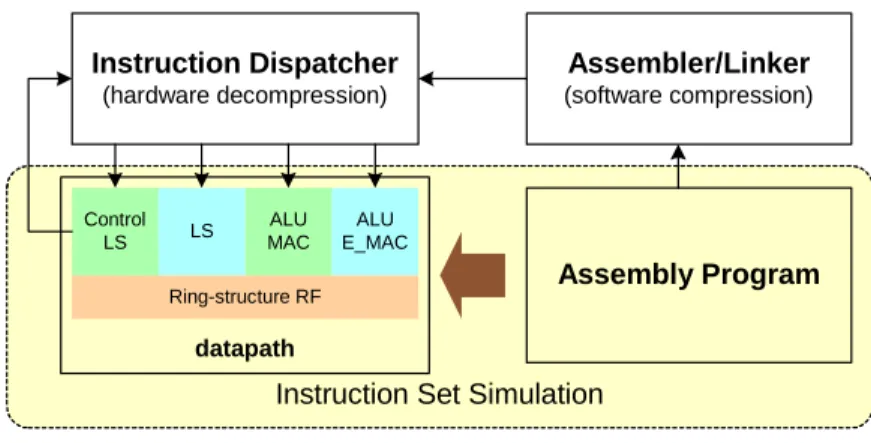
Fig 1 depicts the 2-tier instruction processing with separate control and data
manipulations, which effectively smoothes the instruction flow to the DSP datapath.
The proposed DSP is a four-way VLIW processor with two load/store units and two
ALU/MAC units. The instruction dispatcher handles zero-overhead looping and the
unconditional branches (e.g. jumps and traps) transparently to the datapath, which
receives an instruction packet (including four RISC-like instruction words) per cycle,
regardless of the control flow, except the conditional branches (data-dependent
control), which need the cooperation with the control/LS FU (instruction field 0) of
the datapath. With the proposed ring-structure RF for efficient data exchange among
FU, the proposed DSP processor can easily achieve its peak performance of four
16-bit data operations per cycle, or fifteen RISC-type operations per cycle (including
four effective data manipulations, four data generations, four address updates, and
three branch controls).
Ring-structure RF Instruction Dispatcher (hardware decompression) Control LS ALU MAC LS ALU E_MAC datapath Assembly Program Assembler/Linker (software compression)
Instruction Set Simulation
Fig 1 2-tier instruction processing
In addition to the general assembling and linking, our code generation tool takes
the responsibility for the code compression, while the dispatcher dynamically
recodes the compressed variable-length instruction packets to simplify the target
address calculation in the control flow for a fixed-length header and the remnant
codes, which are stuffed from the beginning and the end respectively into a long
fixed-length instruction bundle. The linker assigns each label in the user’s assembly
program the bundle number with the packet offset, instead of the target address of the
packet directly to simplify control manipulations. Note that the symbolic
instruction-set simulation in the 2-tier instruction processing can be conducted
independently from the instruction encoding and compression schemes in the
3.2 VLIW Datapath with SIMD Capability
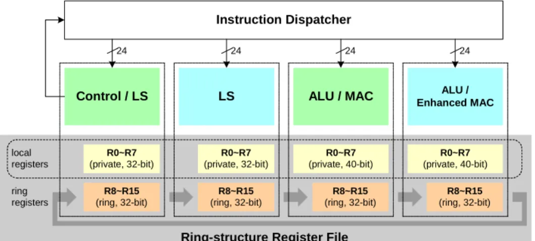
3.2.1 Ring-str uctur e r egister file
A centralized register file (RF) provides storage for and interconnects to each
functional unit (FU) in a general manner and each FU can read from or write to any
register location. For N concurrent FU, the silicon area of the centralized RF grows
as N 3, the delay as N 3/2, and the power dissipation as N 3 [3]. Thus, the RF will soon dominate the area, the delay, and the power dissipation in the multi-issue processors
as the number of FU increases. The communication between FU is usually restricted
by partitioning the RF to reduce the complexity significantly with some performance
penalty. In other words, each FU can only read and write a limited subset of
registers. In this project, we partition the centralized RF into 2N sub-blocks and
separate the interconnection from the RF with an explicit switch network. Each FU
can simultaneously access two sub-blocks, one of which is private (i.e. dedicated to
the FU) and the other is dynamically mapped for inter-FU communications.
Therefore, each sub-block only requires the access ports for a single FU. By the way,
the shared sub-blocks are organized in a ring to reduce the control overheads, where
the dynamic mapping is exposed to the VLIW ISA with log2N offset bits and is directly specified by the programmers for each instruction packet.
The shaded region in Fig 2 shows the ring-structure RF in our proposed 4-way
VLIW DSP processor. Each sub-block has four access ports (2R/2W). Imagine the
four concurrent FU as individual RISC-like processors, and each processor has a
16-element RF. Each RF is partitioned into a private and a shared sub-block, each of
data exchanges among the four FU and are concatenated as a ring with a 2-bit control
to reduce the context for dynamic port mapping. The shared sub-blocks are all
identical and each has eight 32-bit elements (r8~r15). The private sub-blocks (i.e.
local registers) of the control/LS FU have eight 32-bit elements for general-purpose
uses and memory addresses, while those of ALU/MAC have eight 40-bit
accumulators. The port mapping is controlled by the 2-bit ring offset attached to
each instruction packet without any state, which is completely transparent to the FU.
Control / LS LS ALU / MAC Enhanced MACALU /
R0~R7 (private, 32-bit) R0~R7 (private, 32-bit) R0~R7 (private, 40-bit) R0~R7 (private, 40-bit) R8~R15 (ring, 32-bit) R8~R15 (ring, 32-bit) R8~R15 (ring, 32-bit) R8~R15 (ring, 32-bit) local registers Instruction Dispatcher 24 24 24 24 ring registers
Ring-structure Register File
Fig 2 Ring-structure register file
3.2.2 SIMD functional units
The ALU/MAC unit can perform two 16-bit ALU operations simultaneously.
Moreover, it supports two concurrent 16-bit MAC operations with 40-bit
accumulators with the instruction
MAC_V ri, rm, rn,
which executes ri ri+rm.Hi×rn.Hi, and ri+1 ri+1+rm.Lo ×rn.Lo in parallel.
It needs four concurrent accesses to the RF (two reads and two writes respectively).
The index i must be even, with i+1 implicitly specified. Besides, the DSP also
supports powerful double load (store) instructions of the form
which performs two parallel memory accesses (rm Mem[ri], rn Mem[ri+1]) with
concurrent address updates (ri ri+j, and ri+1 ri+1+j). These instructions
require six concurrent RF accesses (including two reads and four writes for loads, or
four reads and two writes for stores). The accesses do not conflict because ri and
ri+1 are local address registers while rm and rn are ring registers that deliver data to
ALU/MAC. They locate in independent register sub-blocks.
Finally, the ALU/enhanced MAC unit supports single-cycle 16-bit complex
MAC/MUL or single-cycle 32-bit MAC/MUL. These instructions exhaust all
multiplication resources (i.e. our DSP totally has four 16-bit multipliers) and prevent
the other ALU/MAC unit from any operation involving multiplication.
3.2.3 Pr ogr amming model
The assembly syntax for our VLIW DSP starts with the ring offset, followed by
the four RISC-like instruction words to form an instruction packet as
ring offset; i0; i1; i2; i3;.
The summary of our instruction set is available in Appendix.
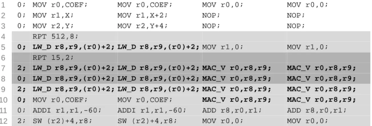
Fig 3 is an illustrating example of a 64-tap finite-impulse response (FIR) filter
that produces 1,024 outputs. The memory subsystem uses half-word addressing and
the input and output data are 16-bit fractional and 32-bit fixed-point numbers
respectively. The RPT instruction (the repeat instruction for zero-overhead looping;
see line 4 and line 6) is carried out in the instruction dispatcher and consumes no
execution cycle of the datapath. Note that only two-level loop nesting is allowed in
our current implementation.
The inner loop (line 7-8) loads four 16-bit inputs and four 16-bit coefficients into
two 32-bit r8 and two 32-bit r9 with the two SIMD LS units respectively, while the
the two ALU/MAC units perform 16-bit SIMD MAC operations of the form
MAC_V r0, r8, r9
for four taps (i.e. r0 r0+r8.Hi×r9.Hi, and r1 r1+r8.Lo× r9.Lo for each
ALU/MAC). After summing up the 32 32-bit products with 40-bit accumulators, r0
are r1 are added together and rounded to the 32-bit r8 in the ring registers. Finally,
two 32-bit outputs are stored in the memory subsystem by the two LS units via r8.
In this FIR example, the outer loop (line 5 and line 7-12) can produce two filter
outputs in 35 cycles. In other words, the proposed DSP can compute 3.66 taps every
cycle.
The conditional branches in our DSP processor evaluate the conditions through
the register ports of control/LS FU, which execute in parallel with the succeeding
instruction packet. Therefore, NOP must be inserted if the access port conflicts.
1 0; MOV r0,COEF; MOV r0,COEF; MOV r0,0; MOV r0,0;
2 0; MOV r1,X; MOV r1,X+2; NOP; NOP;
3 0; MOV r2,Y; MOV r2,Y+4; NOP; NOP;
4 RPT 512,8; 5 0; LW_D r8,r9,(r0)+2; LW_D r8,r9,(r0)+2; MOV r1,0; MOV r1,0; 6 RPT 15,2; 7 2; LW_D r8,r9,(r0)+2; LW_D r8,r9,(r0)+2; MAC_V r0,r8,r9; MAC_V r0,r8,r9; 8 0; LW_D r8,r9,(r0)+2; LW_D r8,r9,(r0)+2; MAC_V r0,r8,r9; MAC_V r0,r8,r9; 9 2; LW_D r8,r9,(r0)+2; LW_D r8,r9,(r0)+2; MAC_V r0,r8,r9; MAC_V r0,r8,r9;
10 0; MOV r0,COEF; MOV r0,COEF; MAC_V r0,r8,r9; MAC_V r0,r8,r9;
11 0; ADDI r1,r1,-60; ADDI r1,r1,-60; ADD r8,r0,r1; ADD r8,r0,r1;
12 2; SW (r2)+4,r8; SW (r2)+4,r8; MOV r0,0; MOV r0,0;
Fig 3 Example: 64-tap FIR Filter
3.2.4 ISA per for mance with exposed r ing-str uctur e RF
This section evaluates the performance degradation due to the access restrictions
of the ring-structure RF, where the port mapping is under the direct control of the
programmers. We have constructed an instruction-set simulator for the proposed
4-way VLIW DSP processor following the assembly syntax described in Section 3.4.
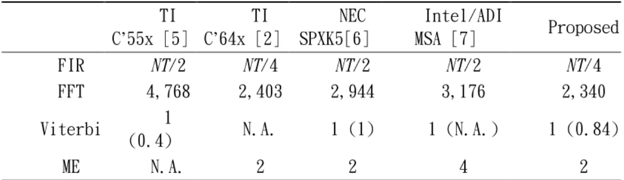
TI C’55x [5] TI C’64x [2] NEC SPXK5[6] Intel/ADI MSA [7] Proposed FIR NT/2 NT/4 NT/2 NT/2 NT/4 FFT 4,768 2,403 2,944 3,176 2,340 Viterbi 1 (0.4) N.A. 1 (1) 1 (N.A.) 1 (0.84) ME N.A. 2 2 4 2
Table 1 summarizes the performance comparisons of the state-of-the-art
high-performance DSP processors and the proposed ISA with the exposed
ring-structure RF. The second row shows the number of cycles required for
N-sample T-tap FIR filtering, which indicates the on-chip MAC resources. The third
row lists the performance of the radix-2 256-point fast Fourier transform (FFT),
which is measured in the number of execution cycles. The maximum ACS
(add-select-compare) operations per cycle are given in the fourth row, which is the
kernel of the Viterbi algorithm. The numbers in parentheses show the results that
consider the load/store overheads when the depth is 16. The performance of TI
C’64s is not included because it has a specific Viterbi coprocessor. Finally, the last
row compares the performance of the motion estimation under the MAE (mean
absolute error) criteria, which is measured in pixels per cycle. The simulation shows
that the performance of our proposed DSP processor is comparable with the
state-of-the-art DSP for various benchmarks if the dataflow can be appropriately
arranged through the ring-structure RF.
3.3 Hier ar chical VLIW Encoding
The poor code density of the VLIW processors comes from the redundancy
inside (1) the fixed-length RISC-like instruction words because most operations do
NOP must be inserted in the corresponding fields of idle functional units (FU). HAT
[8] is an efficient variable-length instruction format to solve the first problem with
simple control flow. We solve the second one with an explicitly specified ‘valid’
bit-field of the instruction packets to remove all NOP codes. Each FU has a
correspondent bit in ‘valid’ to indicate whether it is idle. The variable-word
instruction packets with the variable-length RISC-like instruction words are then
packed into a large fixed-length bundle for easy instruction accesses. The
instruction encoding is described in Section 4.1 with complete instruction formats in
Appendix, of which the layout is for simple decoding illustrated in Section 4.2.
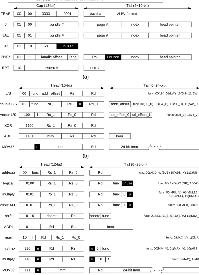
3.3.1 Instr uction for mat
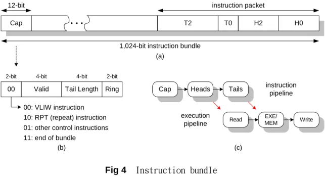
A variable-length RISC-like instruction word is divided into a fixed-length
‘head’ and a variable-length ‘tail’ as HAT [8] to deliver the control information on
demand for the instruction and execution pipelines arranged as Fig 4(c). Fig 7(a)
and (b) in Appendix show the instruction formats for the load/store, and ALU/MAC
units in our DSP. The effective instruction words in an execution cycle (i.e. without
NOP codes) are packed into an instruction packet with a fixed-length control ‘cap’.
The fixed-length caps and the variable-length packets are then placed from the
beginning and the end of the 1024-bit instruction bundle respectively as depicted in
Fig 4 (a). For each instruction packet, the fixed-length heads are placed in order
ahead of the variable-length tails.
In our 4-way VLIW DSP, the cap is a 12-bit control word including the
aforementioned 4-bit ‘valid’ and the 2-bit ring offset. Because an instruction bundle
contains various number of instruction packets, the leading two bits are used to detect
the bundle end. Moreover, they help to recognize the zero-overhead flow controls
to easily locate the next instruction packet for the pipelined instruction dispatcher.
Fig 4(b) shows the packet cap format.
Cap
Cap
Cap T2 T0 H2 H0
instruction packet
1,024-bit instruction bundle
Valid Tail Length Ring 12-bit
2-bit 4-bit 4-bit 2-bit
00: VLIW instruction 10: RPT (repeat) instruction 01: other control instructions 11: end of bundle instruction pipeline Heads Heads Tails Tails Read Read EXE/ MEM EXE/
MEM WriteWrite
execution pipeline 00
(a)
(b) (c)
Fig 4 Instruction bundle
The instruction dispatcher handles the control instructions, which have
fixed-length caps and variable-length tails, but without heads as depicted in Fig 7(a).
Branch instructions re-direct the instruction flow to a new instruction bundle with the
packet index. To easily locate the target instruction packet, the pointer for the first
instruction head is also available in the instruction encoding. Our first DSP
implementation has 128 instruction memory pages, each of which contains 256
bundles (32 Kbytes). In other words, the maximum instruction memory is 4 Mbytes.
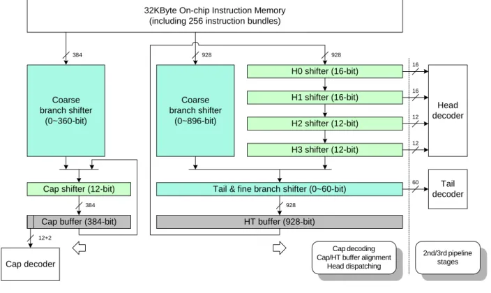
3.3.2 Decoder with incr emental/logar ithmic shifter s
To extract from the instruction bundle the appropriate bit fields for decoding is
complex, especially for the variable-length instruction packets. Instead of large
multiplexers, we utilize incremental and logarithmic shifters shown in Fig 5, where
the decoder operates only on the fixed positions. In the simulations, a bundle
bundle to 32 in our implementation. Thus, the cap decoder only needs to examine
the leading 14 bits of the 386-bit shifter, which shifts out one 12-bit cap constantly
every cycle. The four multiplexers at the right-hand-side Fig 5 shift out the
fixed-length heads depending on the ‘valid’ bits of the cap. The logarithmic tail
shifter follows to shift out all tails of the instruction packet. In brief, the head/tail
shifter is aligned to the next instruction packet at succeeding clock cycle as the 12-bit
cap shifter. Finally, for branch instructions, two coarse logarithmic shifters are used
to align the new instruction bundle with the index and the packet pointer respectively.
Note that the cap and head/tail shifters contain overlapped bits because of the
non-deterministic boundary between caps and packets.
32KByte On-chip Instruction Memory (including 256 instruction bundles)
Cap shifter (12-bit)
Cap buffer (384-bit)
Cap decoder 12+2 384 H0 shifter (16-bit) H1 shifter (16-bit) H2 shifter (12-bit) H3 shifter (12-bit)
Tail & fine branch shifter (0~60-bit)
HT buffer (928-bit) Tail decoder 928 16 16 12 12 Coarse branch shifter (0~896-bit) 928 60 Head decoder 2nd/3rd pipeline stages 2nd/3rd pipeline stages Cap decoding
Cap/HT buffer alignment Head dispatching Cap decoding Cap/HT buffer alignment
Head dispatching 928 384 Coarse branch shifter (0~360-bit)
Fig 5 Instruction dispatcher
3.3.3 Code compr ession
Actually, the HAT format has already been extended for VLIW processors [9].
VLIW-HAT is that we use the explicit ‘valid’ bits in the cap to maintain the
position-coded VLIW that enables distributed decoding, instead of individual dispatch
codes with a complex centralized decoder. For an N-way VLIW processor, our
approach uses N ‘valid’ bits for each packet to dispatch its instruction words. By
contrast, VLIW-HAT requires log2(N+1) bits for each packet to indicate the number of active FU and additional log2N bits of each effective instruction word for FU mapping. Assume the average number of instruction words in a packet is P (0 P N),
and the number of bits for instruction dispatch in VLIW-HAT is log2(N+1)+P log2N. Thus, VLIW-HAT has better compression ratio only for codes with extremely low
parallelism. Moreover, we use the 2-bit control in the cap to indicate the bundle end
instead of specifying the number of packets for each bundle as VLIW-HAT, which
reduces some bits further.
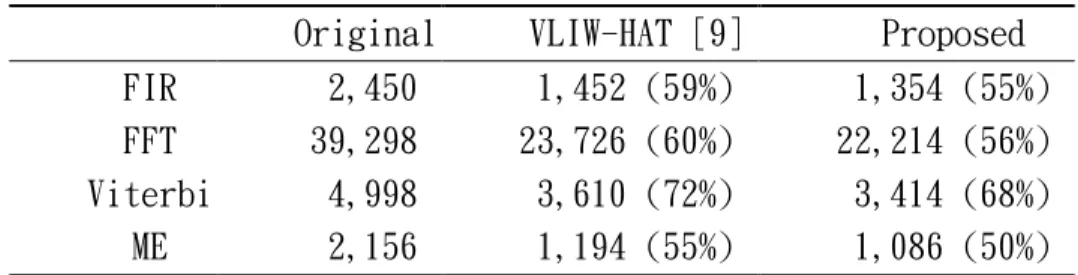
Table 2 summarizes the code sizes for the benchmarks in Table 1 with different
coding schemes. The original codes contain 24-bit fixed-length RISC-like
instruction words, and an instruction packet has 98 bits including the 2-bit ring offset.
VLIW-HAT has a 6-bit packet number in each bundle and a 3-bit instruction number
in each packet, and the instruction formats are very similar to those in Appendix.
Our proposed scheme has better compression ratio for all cases. Moreover, it has
better layout to simplify the decoding than VLIW-HAT.
Table 2 Code size comparison
Original VLIW-HAT [9] Proposed
FIR 2,450 1,452 (59%) 1,354 (55%)
FFT 39,298 23,726 (60%) 22,214 (56%)
Viterbi 4,998 3,610 (72%) 3,414 (68%)
ME 2,156 1,194 (55%) 1,086 (50%)
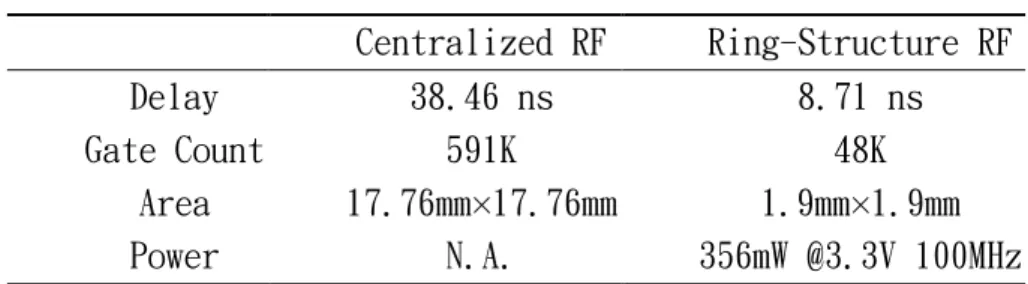
We have implemented in Verilog RTL the ring-structure RF for the proposed
4-way VLIW DSP and the centralized one with the same number of registers. The
designs are synthesized using Synopsys with 0.35ìm cell library and automatically
placed and routed in 1P4M CMOS technology using Apollo. The results are
summarized in Table 3. Our approach reduces the delay and the area by factors of
4.42 and 87.37 respectively. PowerMill is used to estimate the power dissipation of
the ring-structure RF to perform FFT at 100 MHz. We do not have the power
measure for the centralized RF due to the limited tool capability.
Table 3 Comparison of RF structures
Centralized RF Ring-Structure RF
Delay 38.46 ns 8.71 ns
Gate Count 591K 48K
Area 17.76mm×17.76mm 1.9mm×1.9mm
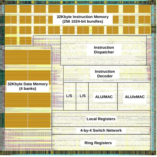
32Kbyte Instruction Memory (256 1024-bit bundles)
32Kbyte Data Memory (4 banks) Instruction Dispatcher Instruction Decoder ALU/eMAC ALU/MAC L/S L/S Local Registers 4-by-4 Switch Netw ork
Ring Registers
Fig 6 Layout of the proposed VLIW DSP
Fig 6 shows the layout of our trial implementation of the proposed 4-way VLIW
DSP processor with 32-Kbyte data and 32-Kbyte instruction memories. The
processor is pipelined into five stages (3-stage instruction pipeline and 3-stage
execution pipeline with one overlapping stage) and operates at 71.43 MHz. The
4. 結論與討論
In this project, we design an efficient VLIW DSP architecture for baseband
processing, where the two major weaknesses of VLIW processors are effectively
improved. We propose a novel ring-structure register file (RF), which saves 91.88%
silicon area of a centralized one, and reduces its access time by 77.35%. The
simulation shows that the ISA with the exposed ring-structure RF has comparable
performance for various DSP kernels with the state-of-the-art DSP processors. The
preliminary results of our trial implementation are very promising. We are currently
working on the custom designs of the register sub-blocks, the 4-by-4 switch network,
and critical components of the datapath. Extensive clock gating will be applied to
reduce the power.
Besides efficient datapath designs, we also improve the poor code density with
the proposed hierarchical VLIW encoding, which reduces redundant bits with
variable-length instruction words and NOP removal. Our simulation shows the
proposed encoding scheme reduces 32%~50% code sizes. Finally, there still exists
redundancy between instruction packets due to loop unrolling and software pipelining
techniques [1], which improve the instruction-level parallelism. The integration of
differential encoding scheme [10] will be studied to remove the repetitive codes for
參考文獻
[1] J. L Hennessy, and D. A. Patterson, Computer Architecture – A Quantitative Approach, 3rd Edition, Morgan Kaufmann, 2002
[2]TMS320C64x DSP Library Programmer's Reference, Texas Instruments Inc., Apr
2002
[3] G. G. Pechanek and S. Vassiliadis, "The ManArray embedded processor architecture," Euromicro Conference, vol.1, pp.348-355, September, 2000
[4] S. Rixner, W. J. Dally, B. Khailany, P. Mattson, U. J. Kapasi, and J. D. Owens, “Register organization for media processing,” International Symposium on High Performance Computer Architecture (HPCA), pp.375-386, 2000
[5]TMS320C55x DSP Programmer ’s Guide, Texas Instruments Inc., July 2000
[6] T. Kumura, M. Ikekawa, M. Yoshida, and I. Kuroda, “VLIW DSP for mobile applications,”IEEE Signal Processing Magazine, pp.10-21, July 2002
[7] R. K. Kolagotla, et al, “A 333-MHz dual-MAC DSP architecture for next-generation wireless applications,” IEEE International Conference on Acoustics, Speech, and Signal Processing (ICASSP 2001), vol. 2, pp.1013-1016,
May 2001
[8] H. Pan and K. Asanovic, “Heads and tails: a variable-length instruction format supporting parallel fetch and decode,”International Conference on Compilers, Architecture, and Synthesis for Embedded Systems (CASES 2001), Nov 2001
[9] H. Pan, High-Performance, Variable-Length Instruction Encodings, Master Thesis,
MIT, 2002
[10] G. Fettweis, M. Bolle, J. Kneip, and M. Weiss, “OnDSP: a new architecture for wireless LAN applications,”Embedded Processor Forum, May 2002
[11] P. Lapsley, J. Bier, A. Shoham, and E. A. Lee, DSP Processor Fundamentals – Architectures and Features, IEEE Press, 1996
[12] Y. H. Hu, Programmable Digital Signal Processors – Architecture, Programming, and Applications, Marcel Dekker Inc., 2002
附錄
Instruction set summary
Mnemonic Action INSTRUCTION DISPATCHER
RPT Repeat the following m packets n times J Jump; unconditional branch
JAL Jump and link JR Jump register
BNEZ Branch on not equal zero TRAP Trap; system call
COMMON TO ALL FIELDS
NOP No operation ADDI Add immediate
XOR Exclusive OR
MOV32 Move 32-bit immediate FIELD 0/1 LH / SH Load/store half word LW / SW Load/store word
LH_D / SH_D Double load/store halfword LW_D / SW_D Double load word
LH_V / SH_V (SIMD) load/store halfword vector FIELD 2/3
MUL 16-bit Hi/Lo multiply
MAC 16-bit Hi/Lo multiply & accumulate ADD Add
SUB Subtract AND AND
OR OR
SLL Shift left logical SRL Shift right logical SRA Shift right arithmetic
BF2 Radix-2 butterfly
MUL_V (SIMD) 16-bit multiply with 32-bit result MUL_16V (SIMD) 16-bit multiply with 16-bit result
MAC_V (SIMD) 16-bit multiply with 40-bit accumulate ADD_V (SIMD) 16-bit add
SUB_V (SIMD) 16-bit subtract ABS_V (SIMD) absolute value SRA_V (SIMD) shift right arithmetic
MIN_V (Subword) select the small element MAX_V (Subword) select the large element PACK Merge low 16-bit of two registers
SPECIFIC TO FIELD 3
CMUL 16-bit complex multiply with 32-bit result CMUL_16V 16-bit complex multiply with 16-bit result
CMAC 16-bit complex multiply with 40-bit accumulate MUL32 32-bit multiply
MAC32 32-bit multiply & accumulate 10 repeat # instr # RPT 00 00 0000 syscall # TRAP 0001 01 00 bundle # page #
J index head pointer
01 01 bundle # page #
JAL index head pointer
01 10 Rs
JR unused
01 11 bundle offset Rs
BNEZ Ring index head pointer
Cap (12-bit) Tail (4~16-bit)
unused
VLIW format
(a)
00 func addr_offset Rs Rd func: 00(LH), 01(LW), 10(SH), 11(SW)
01 func Rd_1 Rs Rd_0 addr_offset func: 00(LH_D), 01(LW_D), 10(SH_D), 11(SW_D)
100 f Rs_1 Rs_0 Rd ad_offset_0 ad_offset_1 func: 0(LH_V), 1(SH_V)
1101 Rs Imm.
ADDI Rd
111 u Imm.
MOV32 24-bit Imm.
1100 Rs_1 XOR Rs_0 Rd Tail (0~24-bit) Head (16-bit) L/S vector L/S double L/S Rd Imm. u (b)
00 func Rs_1 Rs_0 Rd func: 00(ADD),01(SUB),10(ADD_V),11(SUB_V) unuse Tail (0~28-bit) Head (12-bit) add/sub 0100 Rs_1 Rs_0 Rd logical func 0110 shamt func shift Rs 0111 Rd ADDI Rs Imm.
shamt func: 00(SLL),01(SRL),10(SRA),11(SRA_V)
111 Imm.
MOV32 Rd 24-bit Imm.
110 Rd Rs u 10 f func: 0(MAC), 1(MUL)
multiply
110 Rd Rs u 0 func
min/max func: 00(MIN_V), 01(MAX_V), 10(ABS_V)
10 Rd
mac Rs_0 func: 0(MAC_V), 1(CMAC)
func: 00(AND), 01(OR), 10(XOR)
0101 Rs_1 Rs_0 Rd
multiply func func: 00(MUL_V), 01(MUL16_V)
10(CMUL), 11(CMUL16)
Rs_1
Rs_1 Rd
other ALU Rs_0 func func: 00(PACK), 01(BF2)
f 0101 u u 0 1 u u u (c)