國 立 交 通 大 學
電控工程研究所
碩士論文
SOI 基板上利用簡單下壓方式組裝之微光學讀取頭
A MEMS-Based Optical Pickup Unit Assembled by
Simple Push Operation on SOI Wafers
研究生 :林健安
指導教授:邱一 博士
SOI 基板上利用簡單下壓方式組裝之微光學讀取頭
A MEMS-Based Optical Pickup Unit Assembled by
Simple Push Operation on SOI Wafers
研 究 生:林健安 Student: Chen An Lin
指導教授:邱一 Advisor: Yi Chiu
國立交通大學 電機學院
電控工程研究所
碩士論文
A Thesis
Submitted to Department of Electrical Control Engineering
College of Electrical Engineering
National Chiao Tung University
In Partial Fulfillment of the Requirement
For the Degree of
Master
In
Electrical and Control Engineering
July 2010
中文摘要
近年來在半導體產業的發展之下,微機電製程技術有許多重大的發 展。對於光學資料儲存系統而言,微光機電技術(Micro Optical Electro Mechanical System)正是提供製造更小更輕的光學資料儲存系統的一個好 方法。
我們的目標是要製作一微光學資訊平台,此微光學平台是以數個三維 斜面結構以及其他組裝於此平台上的光學元件所組成,因此採用應力幾乎 為零且結構較厚的SOI (Silicon On Insulator)基板製作微鏡面,避免一般利 用多晶矽製作時可能發生的翹曲現象。 本實驗室之前已提出利用下壓動作即可成功組裝 45°微鏡面的設計, 本論文將利用此下壓組裝方法,組裝4 種不同角度的斜面鏡以證實此方法 可用於任意角度的斜面鏡組裝,符合未來在光學平台應用中不同角度三維 微結構的需求。本論文亦對於原始 45°結構的誤差問題加以探討並提出改 善方式,使得角度從45.9 ± 0.2° 改善為 45.4 ± 0.2°。最後,本論文並且提 出且成功製造出135° 三維微結構,平均角度為 135.6 ± 0.2°,可應用在本 論文中提出的光學讀取頭架構。此光學讀取頭的模擬結果以及設計原理在 論文中有詳細的說明,是利用全像光學元件(HOE)來達到像散以及分光的 功用,取代傳統光學讀取頭中利用體積較大的柱面鏡以及分光鏡,進而達 到微型化的目的。此全像光學元件(HOE)以微機電製程的方法製造於光學 平台的斜面結構上,它的表面輪廓以及光學特性在論文中都已經過實驗量 測並驗證。完整的光學平台架構正處於製程的最後階段。
Abstract
Recently, the Micro Electro Mechanical Systems (MEMS) technology has many important developments with the rapid progress in the semiconductor industry. The requirement of miniaturization and lightness pushes the development of smaller and lighter optical data storage systems. Micro optical pickup head fabricated by Micro-Opto-Electro-Mechanical System (MOEMS) technology is one of the methods to realize portable high-capacity optical storage systems.
In this thesis, micro optical pickup head on an micro optical bench is composed of nonvertical micro mirrors and other optical components bonded on the optical bench. Silicon on insulator (SOI) wafers with almost zero stress are used to avoid stress-induced curvature for optical applications.
In our previous study, 45° structures were assembled using a novel simple push operation. Micromirrors with four different angles were pushed up by probes to demonstrate the assembly method for arbitrary angles in this thesis. The angular deviation of the 45° structures was studied with different width of the support arms. The angles of 45° structures were improved from 45.9°±0.2° to 45.4°±0.2°. The design and assembly of 135° mirrors were verified and used in the proposed optical pickup head of this thesis. The devices were fabricated with an average angle of 135.6°± 0.2°. The simulation results and the design principle of the MEMS-based optical pickup head are present. A holographic optical element is used in the optical bench and fabricated on the nonvertical mirror. The surface profile and optical properties of the fabricated holographic were measured. The fabrication of the optical bench is in progress.
致謝
結束了碩士班的研究生活,懷著感激的心謝謝所有幫助過我的人,我要 感謝我的父母,讓我能無憂無慮的完成碩士學業。再來要感謝的是我的指導教授 邱一老師, 在實驗上給予我許多專業的建議及指導,也教導了我發現問題及解 決問題的方法,學習到了許多研究與處事應有的態度,使得我的實驗能夠順利進 行。 非常感謝我的口試委員方維倫老師和施錫富老師,能再繁忙之餘對我的論文 提供指導建議和鼓勵。 還有感謝實驗室學長昌修、弘諳、子麟、昇儒對我的指導,讓我能傳承你們 的經驗前進,以及電控所的學長振鈞、冠州和動機所的學長信瑜,感謝你們總是 在繁忙中還能夠給予我許多實驗上的建議。感謝奈米中心徐小姐、范小姐、國華、 范先生的幫忙,讓我能迅速完成許多的製程實驗。 要感謝的當然還少不了實驗室的夥伴,感謝經富、哲明、俊宏、鴻智、姿穎、 政安、彥傑、彥霆陪我度過在實驗室的日子,你們總是能互相打氣維持實驗室的 良好氣氛讓我把做實驗所帶來的煩悶一掃而空。 最後我要再次感謝我的老爸老媽以及我的家人朋友們,感謝你們的支持和鼓 勵,不論是學術或是待人處世都讓我在碩士班的生涯學到了很多。最後也謝謝這 段時間培育我成長的交通大學,珍重再見。Table of Content
中文摘要...iv
Abstract……..……….………...…...…………..…...ii
誌謝...………..…..………..…...iii
Table of Content ...iv
List of Figures...vi List of Tables...xii Chapter 1 Introduction...1 1-1 Motivation...1 1-1-1 Waveguide type ...3 1-1-2 Planar type...4
1-1-3 Free-space staked type ...4
1-1-4 Optical pickup for small form factor drives ...5
1-2 Review of Micro Assembly ...7
1-2-1 Microfabricated hinges...7
1-2-2 Three dimensional MEMS by active assembly ...8
1-2-3 Three dimensional MEMS by self-assembly...11
1-2-4 Manual or robot-assisted assembly...17
1-3 Objective and organization of the thesis...24
Chapter 2 Principle and Design...26
2-1 Introduction...26
2-2 Mirror with arbitrary angles...26
2-2-1 30o, 45o , and 60o mirrors ...26
2-2-2 135o mirrors ...32
2-3 Optical bench and MEMS-based optical pickup head...34
2-3-1 Simulation of the MEMS-based optical pickup head ...35
2-3-2 Diffractive efficiency of HOE...39
2-3-3 Layout design...45
2-3-4 Summary ...48
Chapter 3 Fabrication Process...49
3-1 Fabrication process ...49
3-2-2 Backside ICP etching ...62
3-3 Summary ...67
Chapter 4 Measurement and Results ...68
4-1 30°, 45°, and 60° structures ...68
4-2 135° structures ...77
4-3 Holographic optical element (HOE) ...81
4-3-1 Surface profile...81
4-3-2 Optical measurement ...83
4-3-3 Discussion...85
4-4 Summary ...87
Chapter 5 Conclusion and Future work ...88
5-1 Conclusion ...88
5-2 Future work...88
5-2-1 Nonvertical devices...88
5-2-2 Optical bench ...89
List of Figures ______
Figure 1-1 Conventional optical pickup head...2 Figure 1-2 On-chip optical pickup head system [1]...2 Figure 1-3 Waveguide type optical pickup head, (a) fabrication process, (b) schematic
[2]...3 Figure 1-4 Planer type optical pickup head, (a) side view, (b) top view [3]...4 Figure 1-5(a) Schematic of stacked optical pickup head, (b) cross section of the
silicon-base suspended optical element [4]...5 Figure 1-6(a) Schematic of integrated optical pickup, (b) picture of silicon bench [5].6 Figure 1-7 Optical path of integrated optical pickup [5] ...6 Figure 1-8(a) Fabrication process of micro hinges, (b) SEM micrograph of a hinged
structure [7]...8 Figure 1-9(a) Crossed sectional view of SDA, (b) working principle of SDA [8].. ...9 Figure 1-10 SEM of a free-rotating hinged micromirror lifted by an array of SDA [9]..
...9 Figure 1-11(a) SEM of the automated assembly system connected to a scanning
mirror, (b) basic assembly process [10] ...10 Figure 1-12(a) Schematic of the lateral thermal actuator, (b) SEM of the vertical
thermal actuator [10]...11 Figure 1-13 SEM of (a) the self-engaging locking mechanism, (b) an assembled
corner cube reflector [10]...11 Figure 1-14 Magnetic force assembly...12 Figure 1-15(a) Side view of a hinged microstructure in an external magnetic field, (b)
hinge with different dimensions and sensitivity factors [12]...13 Figure 1-16 Step-by-step photographs of the four-step sequential assembly [12] ...13
Figure 1-18 Batch assembly by centrifugal force: (a) an array of bridge structures, (b)
an array of micromirrors [13] ...14
Figure 1-19 Schematic of thermokinetic force assembly ...15
Figure 1-20 Assembly by thermokinetic force: (a) an array of micromirrors, (b) corner cube reflectors [14] ...16
Figure 1-21(a) Assembled structures by combining bimorph beams with locking mechanism, (b) locking mechanism [15]...16
Figure 1-22 Surface tension powered assembly by (a) photoresist [16], (b) solder [17]. ...17
Figure 1-23(a) MEMS electrothermal gripper, (b) MEMS end-effector [19] ...18
Figure 1-24(a) Overview of whole chip where assembly is taking place, (b) close up of the de-tether process, (c) a micropart is picked off the substrate, (d) schematic of microconector, (e) the connector being inserted into the socket [19]...19
Figure 1-25(a) SEM image, (b) optical micrograph of assembled device [19] ...20
Figure 1-26 Hingeless device concept [20] ...21
Figure 1-27 Schematic assembly sequence [20]...21
Figure 1-28(a) Optical micrographs of the assembly process (b) SEM image of 90° out-of-plane structures [20]...21
Figure 1-29 Assembly process with one-push operation [21] ...23
Figure 1-30(a) Schematic view of the V-shaped hinge after assembly, (b) top view..23
Figure 1-31 SEM images and optical micrograph of assembled devices, (a) Mirror is flipped by one-push operation, (b) a corner cube reflector. [21] ...23
Figure 1-32 Schematic of the MEMS-based optical pickup head in this thesis ...25
Figure 2-2 Assembly process of the 45o device ...28
Figure 2-3 Layout design of (a) 60o device, (b) 30o device ...28
Figure 2-4 Form and dimensions of cross sections...29
Figure 2-5 Schematic of static equilibrium after assembly ...31
Figure 2-6 Schematic of assembled 45° mirror with bent support ...31
Figure 2-7(a) Layout design of 135o device, (b) 3-D model...32
Figure 2-8 Assembly process of the 135o device ...33
Figure 2-9 Schematic of the MEMS-based optical pickup head ...34
Figure 2-10 Zemax simulation of the MEMS-based optical pickup head ...35
Figure 2-11 Zemax simulated optical spot on the disk ...35
Figure 2-12 Simulated optical spot on the photodetector with various amount of defocus ...37
Figure 2-13 Schematic of the astigmatic method ...39
Figure 2-14 Simulation of the S-curve...39
Figure 2-15 Schematic of diffraction theory...41
Figure 2-16 (a) Schematic and (b) phase distribution of the reflective linear phase grating ...42
Figure 2-17 Schematic of the reflective type linear phase grating on 135o mirror...43
Figure 2-18 Calculation of diffraction efficiency ...44
Figure 2-19 Layout of the holographic optical element...46
Figure 2-20 Schematic of the optical bench after assembly ...46
Figure 2-21 Optical simulation of the system, (a) side-view, (b) top-view ...47
Figure 2-22 Layout of optical bench...48
Figure 3-1 Fabrication process...50
Figure 3-3 Problems in Si3N4 photolithography ...61
Figure 3-4 After the silicon nitride RIE, (a) silicon nitride remained on the release holes, (b) silicon nitride was etched completely...62
Figure 3-5(a) Bending of the mirror plate, (b) break of the mirror plate after the backside ICP etching...63
Figure 3-6 Bending measurement by WYKO before release process. ...63
Figure 3-7 Bending measurement by WYKO after release process ...64
Figure 3-8 Broken silicon oxide at the big through-wafer hole...65
Figure 3-9 Device layer is etched in the backside ICP process ...65
Figure 3-10 Schematic of original and redesigned backside etching under the mirror plate, (a) big hole, (b) meshed structure, (c) entire substrate is unetched....66
Figure 3-11 Fabricated devices, (a) an array of 45° device, (b) an array of 135° device, (c) side view of an assembled 135° mirror, (d) holographic optical element (HOE)...67
Figure 4-1 Assembly process of a 45° mirror without hinges, (a) two probes were aligned with the push pads before assembly, (b) the support was pushed by Probe 1, (c) the mirror was pushed by Probe 2, (d) remove Probe 1 so that the support lie on the mirror, (e) Probe 2 was removed, (f) Probe 1 was removed...69
Figure 4-2 An assembled 30° device, (a) top view, (b) side view, (c) interlock, (d) torsional beam connected to the mirror plate...70
Figure 4-3 An assembled 45° device, (a) top view, (b) side view ...70
Figure 4-4 An assembled 60° device, (a) top view, (b) side view, (c) interlock, (d) torsonal beam of the mirror plate with mechanical stop...71
Figure 4-5 An assembled mirror at 30.6°...72
Figure 4-6 An assembled mirror at 45.4°...73
Figure 4-7 An assembled mirror at 60.7°...73
Figure 4-8 Bent supports, (a) side view, (b) perspective view [22]...75
Figure 4-9 Bending of supports in prior design after assembly, (a) 3-D profile, (b) 2-D analysis...75
Figure 4-10 Bending of improved supports in this work after assembly, (a) 3-D profile, (b) 2-D analysis...76
Figure 4-11 Assembly process of a 135° mirror without hinge, (a) two probes aligned before assembly, (b) mirror plate pushed by Probe 1 and held by Probe 2 from the other side ...77
Figure 4-12 An assembled 135° device, (a) top view, (b) side view, (c) push pad of mirror plate, (d) interlock, (e) torsional beams of mirror plate, (f) torsional beams and mechanical stops ...79
Figure 4-13 An assembled mirror at 135.4°...80
Figure 4-14 Optical micrographs of the fabricated HOE ...82
Figure 4-15 SEM micrographs of the HOE, (a) fabricated HOE, (b) period of HOE, (c) linewidth of the etching area, (d) linewidth of the unetching area ...82
Figure 4-16 AFM measurement results...83
Figure 4-17 Illustration of the optical measurement...84
Figure 4-18(a) Experimental setup, (b) highlight of the HOE...84
Figure 4-19 Diffraction optical spot projected on the screen ...85
Figure 4-20 Comparison of diffraction efficiency between the measurement and theoretical curve...86
Figure 5-2 Fabricated (a) PCB, (b) holder...91 Figure 5-3 (a) Schematic of assembled optical pickup unit, (b) test experiment
showing PCB, holder and objective lens ...91 Figure 5-4 Bonding process of laser diode, (a) a release sample and a mirror plate
before assembly, (b) overlayed image of the laser diode, (c) apply thermal cure adhesive on the laser diode position, (d) bond the laser diode by
List of Tables _____
Table 2-1 Calculation of angular deviation...31
Table 3-1 Comparison of bending mirror plate...64
Table 4-1 Angle measurement of the 30° device (resolution: 0.2°)...72
Table 4-2 Angle measurement of the 45° device (resolution: 0.2°)...723
Table 4-3 Angle measurement of the 60° device (resolution: 0.2°)...74
Table 4-4 Comparison of bending support with different design, (a) x-axis, (b) y-axis. ...76
Table 4-5 Angle measurement of the 135° device (resolution: 0.2°)...80
Table 4-6 Comparison of design values and AFM measurement results of the HOE .83 Table 4-7 Measurement results of diffraction optical intensity and etching depth...85
Chapter 1 Introduction
1-1 Motivation
The progress of information technology has increased the demand for data storage day by day. Portable digital devices such as cellular phones, MP3 players and personal digital assistants (PDA) have also found a rapidly increasing market in recent years. Increasing the data storage density and reducing the device size is important for these mobile storage devices. In addition, it is also very crucial to obtain fast access speed of information. Optical data storage systems can achieve these requests.
Optical pickup heads are the most important part in the optical data storage systems. Conventional optical pickup heads are usually composed of laser diodes, grating plates, beam splitters, collimators, reflective mirrors and objective lenses, as shown in Figure 1-1. A beam of light emitted from the laser diode passes through a diffraction grating and diffracted beams are produced. The zeroth-order beam and first-order beams can be used to read data and track the spot respectively. Then, the light passes through the beam splitter and is converted into a parallel beam by the collimator lens. The beam becomes circularly polarized after passes through the quarter wave plate. The beam is then focused on the surface of the disc by the objective lens. The reflected beam becomes linear polarized in the orthogonal direction with respect to the incident beam and is reflected into the photodetector by the polarizing beam splitter. Finally, the photocurrent can be measured by the current detection circuits.
Figure 1-1 Conventional optical pickup head.
In the past years, miniature optical pickup heads have been fabricated by Micro Electro-Mechanical Systems (MEMS) technology. The free-space micro-optical bench is an example of this technology, as shown in Figure 1-2 [1]. The pickup head is composed of a semiconductor laser, a collimator lens, two focusing lens, a beam splitter and two 45o reflectors. The optical bench is fabricated with two polysilicon structure layers and micromachined hinge technology. Compared with the conventional bulk optical pickup heads, the miniaturized optical bench has the advantaged such as reduced size, weight, cost and enhancement of flexibility.
Figure 1-2 On-chip optical pickup head system [1].
Micro-Fresnel lens
Beam-splitter 45o reflector
In addition to the free-space optical pickup head system, there are other types of miniature optical pickup head such as the waveguide type, planar type and free-space stacked type. These miniature optical systems are reviewed in the following sections.
1-1-1 Waveguide type
The waveguide-type optical pickup head is a two dimensional device where light propagates in the planar waveguides in a substrate. All the components can be defined by photolighthography simultaneously, as shown in Figure 1-3. Figure 1-3 (a) shows the fabrication process of the waveguide device. Figure 1-3 (b) shows the schematic of a waveguide optical pickup head [2]. The waveguide is formed with a silicon nitride guiding layer and a silicon oxide buffer layer on a silicon substrate. The guided wave diverging from the laser diode (LD) is focused by the focusing grating coupler into a point on the disk. Then the twin grating focusing beam splitter divides the reflected wavefront into halves, deflects, and focuses into photodetectors. The current signals from the photodetector can be used for readout, focus and tracking signals.
(a) (b)
Figure 1-3 Waveguide type optical pickup head, (a) fabrication process, (b) schematic [2]. Silicon SiO2 PR Photo- lithography RIE- etching Remove PR Si3N4
1-1-2 Planar type
The construction of the planer optical pickup head is shown in Figure 1-4 [3]. The system is composed of four diffractive optical elements integrated on the glass substrate. The light propagates in the glass substrate and then is focused on the disk. The top and bottom of the glass substrate is coated with metal as the reflective surface. The laser diode and the photodetector are mounted on the bottom surface of the substrate. First, a laser beam emitted from the laser diode is couple into the substrate and follows a zigzag optical path. The zeroth-order beam in the forward optical path is focused on the disk by the tramission off-axis objective lens. On the returning path, the first-order diffracted beam is generated by the reflection-focusing beam splitter and projected onto the photodetector. Then the focusing error signal and tracking error signal can be obtained from the photodetector.
(a) (b)
Figure 1-4 Planer type optical pickup head, (a) side view, (b) top view [3].
1-1-3 Free-space stacked type
The free-space stacked optical pickup head is shown in Figure 1-5 [4]. The system is composed of a semiconductor edge-emitting laser source, a 45o bulk silicon reflector, a grating, an holographic optical element (HOE) and aspherical Fresnel lenses. A laser beam is emitted from the laser diode and reflected by the 45o silicon bulk-micronachining mirror. Then the laser is split into three separate beams after
pass through the grating, the two first-order diffracted beams are used for tracking servo control. After being collimated by a Fresnel lens, the beams are eventually focused on the disk by another set of Fresnel lenses. The three beams reflected back from the disk are deflected by the HOE and projected on the photodetector. The 45o bulk silicon reflector is formed from a <100> silicon wafer by anisotropic etching with KOH/IPA etchant. The other optical components such as gratings, HOEs, and Fresnel lenses are formed in silicon nitride film suspended on a silicon substrate and then stacked by chip bonding, as shown in Figure 1-5 (b).
(a) (b)
Figure 1-5 (a) Schematic of stacked optical pickup head, (b) cross section of the silicon-base suspended optical element [4].
1-1-4 Optical pickup for small form factor drives
Samsung and Yon sei university proposed an optical pickup for small form factor drives [5]. The optical pickup is composed of a blue laser diode, a photodetector, and a silicon optical bench. Figure 1-6 (a) and Figure 1-6 (b) show the schematic and photograph of the optical pickup. Figure 1-7 shows the optical path of this optical pickup. After the light emitted from the laser diode is reflected by a 45o mirror, it
passes through a polarized holographic optical element with a quarter wave plate and is focused onto the disc. The light returned from the disc is sent to the photodetector by the polarized holographic optical element and the 64o mirror. Focus and tracking error signals are obtained by astigmatic and push-pull methods. The dimensions of the complete optical pickup are height = 1.9 mm, width = 2.2 mm, and length = 6.6 mm.
(a) (b)
Figure 1-6 (a) Schematic of integrated optical pickup, (b) picture of silicon bench [5].
1-2 Review of Micro Assembly
Ever since the microfabricated hinge made the out-of-plane structures possible, many researchers have been working on 3-D assembly techniques. In addition to manual assembly, “active-assembly” and “self-assembly” are two main techniques. The active assembly method uses actuators such as scratch drive actuators or thermal actuators for assembly. The self-assembly method uses the forces derived from an energy field such as thermal, centrifugal force, or a magnetic field. Furthermore, residual stress and surface tension are also used for self-assembly. Recently, high precision robotics is used for automatic assembly process by standard or specially designed equipments. Some techniques for microassembly are reviewed in this section.
1-2-1 Microfabricated hinges
Surface micromachining [6] is the most common technique for fabricating MEMS devices. The standard surface micromachining has high planar resolution, but low vertical resolution and limited vertical range (usually less than 5 μm). These disadvantages have limited the development of three-dimensional designs until Pister et al. proposed the micro hinge structures [7]. A two-layer polysilicon process with oxide sacrificial layers was used to fabricate the hinge. This component enables surface micromachined structures to rotate out-of-plane by using the hinge structures. The schematic view of the hinge process and the SEM photo of a hinged structure are shown in Figure 1-8. This microhinge technique is a great breakthrough of surface micromachining for three-dimensional designs.
(a) (b)
Figure 1-8 (a) Fabrication process of micro hinges, (b) SEM micrograph of a hinged structure [7].
1-2-2 Three dimensional MEMS by active assembly
The active assembly methods by using actuators such as scratch drive actuators and thermal actuators are reviewed in this section.
Scratch drive actuator active assembly
The scratch drive actuator (SDA), as shown in Figure 1-9, consists of a plate, a bushing, an insulator layer and a substrate electrode [8]. When a voltage is applied, the plate is pulled down toward the substrate by the electrostatic force. A part of the plate is pulled down to contact with the surface of insulator. The warp of plate causes the bushing to tilt and shifts a small distance. When the voltage is removed, the plate and the bushing return to their original positions, but translate forwards by a small distance. By driving the device with a periodic voltage, the SDA can go forward to a position decided by the frequency and amplitude of the driving signal. Figure 1-9 illustrates the structure and the working principle of the SDA [8]. Figure 1-10 shows a micromirror assembled by using an array of SDA [9].
Plate Poly-2 Hinge pin Poly-1 Silicon PSG PSG
(a) (b)
Figure 1-9 (a) Crossed sectional view of SDA, (b) working principle of SDA [8].
Figure 1-10 SEM of a free-rotating hinged micromirror lifted by an array of SDA [9].
Thermal actuator active assembly
Thermal actuators are also used in active assembly [10]. Figure 1-11 (a) shows the micro assembly system connected to a scanning mirror. The system consists of three parts: a linear assembly motor parts (a-c in Figure 1-11 (a)), a vertical actuator parts (d in Figure 1-11 (a)), and a self-locking mechanism part (e in Figure 1-11 (a)). The basic operation of the system is shown in Figure 1-11 (b). Initially, all components are on the surface of the substrate. The vertical thermal actuator is then used to lift the free end of the flip-up plate to form a triangle. The lateral thermal actuator then drives the base of the lift arm toward to the base of the flip-up plate, thus rotating the flip-up
Plate
Bushing Insulator Substrate
plate around its hinge. Finally, the microstructure is positioned by self-engaging locking mechanism. Figure 1-12 (a) and (b) show the schematic of lateral thermal actuator and the SEM photograph of vertical thermal actuator, respectively. The lateral thermal actuators function by ohmic heating. The resulting displacement is shown in Figure 1-12 (a). The vertical thermal actuator consists of two parallel polysilicon beams separated by an air gap. At one end, the beams are connected together with a via, whereas at the other end, each arm is separately anchored to the substrate. Again, the hot arm has both higher electrical and thermal resistance than the cold arm due to the smaller width. As the hot arm expands, it drives the tip of the actuator downward towards the substrate. This results in the bowing in Figure 1-12 (b). When the current is removed from the system, the tip of the actuator deflects back away from the substrate and passes its original position. The back bending of the thermal actuator can apply an out-of-plan force to lift the structures. Figure 1-13 shows the SEM photos of the self-engaging locking mechanism and the assembled corner cube reflector.
(a) (b)
Figure 1-11 (a) SEM of the automated assembly system connected to a scanning mirror, (b) basic assembly process [10].
Lift Arm Flip-up plate
Lateral force
(a) (b)
Figure 1-12 (a) Schematic of the lateral thermal actuator, (b) SEM of the vertical thermal actuator [10].
(a) (b)
Figure 1-13 SEM of (a) the self-engaging locking mechanism, (b) an assembled corner cube reflector [10].
1-2-3 Three dimensional MEMS by self-assembly
In addition to the active assembly by actuators, self-assembly uses the force derived from an external energy field or the intrinsic force of the fabricated structures to flip the microstructures out of plane. Self-assembly by the magnetic force, centrifugal force, thermokinetic force, residual stress, and surface tension are reviewed in this section.
Magnetic force assembly
Figure 1-14 shows the principle of employing the magnetic force to lift hinged structures out of plane. Magnetic material such as Permalloy is electroplated on the
Flip-up plate Keyhole Tether Hot arm Cold arm
hinged flap. When an external magnetic field is applied, the hinged flap rotates around the pin axis. The rotation angle is determined by the volume of the magnetic material and strength of the applied magnetic field. Sequential assembly can be achieved by changing the magnetic field strength with different volumes of the magnetic material on the flaps [11]. Recently, Iwase et al. proposed another method of multi-step sequential assembly by changing the geometry of the elastic hinges, as shown in Figure 1-15 [12]. Permalloy was electroplated on the plate which was connected by elastic hinges on one side to the substrate, as Figure 1-15 (a) shows. It was found that a dimensionless factor that depended on its shape determined the sensitivity of rotation of the hinged structures to the magnetic field. The volume of the magnetic material and the dimension of the elastic hinges defined the sensitivity factor, as Figure 1-15 (b) shows. When the hinged structure is placed in a magnetic field, the rotation angle of the plate is proportional to the sensitivity factor. Therefore, sequential assembly can be achieved by designing elastic hinges with different sensitivity factors. An example is shown in Figure 1-16. As the applied magnetic field Hext is increased gradually, the plate with the largest sensitivity factor will rise to 90o first. With increased Hext, the other plates with smaller sensitivity reach 90o and each plate is interlocked by the friction force.
Figure 1-14 Magnetic force assembly.
Hinge Pin
Hext θ
(a) (b) Figure 1-15 (a) Side view of a hinged microstructure in an external magnetic field, (b)
hinge with different dimensions and sensitivity factors [12].
Figure 1-16 Step-by-step photographs of the four-step sequential assembly [12].
Centrifugal force assembly
For microscale components, inertial forces such as gravity are usually neglected when compared with surface forces or friction forces. As an inertial force, the centrifugal force can overcome surface forces and friction forces since it is proportional to the square of the rotating speed. Therefore, the centrifugal force can
LH
be used to raise the hinged surface micromachined structures [13]. The concept of this method is illustrated in Figure 1-17. The chip is attached on the surface of rotational disk and is perpendicular to the rotational axis. The hinged structure will be raised out of plane when the rotation starts, as shown in Figure 1-17. Then the microstructure is locked by the latch mechanism. Figure 1-18 shows the batch assembly by using the centrifugal force.
Figure 1-17 Schematic of the concept for centrifugal force assembly.
(a) (b)
Figure 1-18 Batch assembly by centrifugal force: (a) an array of bridge structures, (b) an array of micromirrors [13].
Rotational axis
ω
Rotational
Thermokinetic force assembly
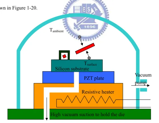
Thermokinetic force can be used to assemble 3-D structures by heating the surface of devices [14]. Figure 1-19 shows the principle and experimental apparatus for raising structures by thermokinetic force. The assembly mount was placed in a vacuum chamber with low pressure in molecular flow regime. The chip was held on the PZT plate by high vacuum suction. The PZT plate was soldered to a hot plate with temperature control to adjust the substrate temperature. The PZT plate was used to overcome the hinge friction by apply a small vibration with high frequency. Since the average velocity of gas molecules bombarding the die surface and flaps are proportional to the temperature, a differential pressure causes the out-of-plane force. Since the temperature of the die surface is larger than that of the vacuum ambiance, the flaps can be lifted out of the substrate and assembled in the upright position, as shown in Figure 1-20.
Figure 1-19 Schematic of thermokinetic force assembly. Silicon substrate
Resistive heater
Vacuum pump
High vacuum suction to hold the die PZT plate
Tsurface Tambient
(a) (b)
Figure 1-20 Assembly by thermokinetic force: (a) an array of micromirrors, (b) corner cube reflectors [14].
Stress-induced assembly
Residual stress can lead to curvature of relearned surface-micromachined structural layers. The bending of released microstructures can be used as motive force to assemble 3-D micro structures. In Figure 1-21, a typical assembly mechanism is composed of stress-induced bimorph beams and locking components [15].
(a) (b)
Figure 1-21 (a) Assembled structures by combining bimorph beams with locking mechanism, (b) locking mechanism [15].
Surface tension powered assembly
Surface tension can be used for self-assembly [16]. Meltable materials such as photoresist or solder are first patterned on the rotational joint. When the photoresist or solder is heated and reflown, it changes into a spherical shape to minimize surface energies, and thus the plate is flipped up. The final rotational angle is determined by the geometry of the meltable material. Some complex 3D microstructures can be constructed with appropriate locking latches. Figure 1-22 shows the assembled micromirror by reflow of photoresist and solder [16, 17].
(a) (b)
Figure 1-22 Surface tension powered assembly by (a) photoresist [16], (b) solder [17].
1-2-4 Manual or robot-assisted assembly
Manual assembly by using microprobes is the first method for raising 3-D mcrostructures; but it is time consuming and has low yield. In recent years, automatic robotic systems are used to pick and place microstructures for automatic assembly. These assembly techniques are reviewed in this section.
Robot-assisted assembly
High precision robots can be used to assemble 3-D microstructures by integrating microgrippers [18] or non-actuated end-effectors [19] on the robotic arms, as shown in Figure 1-23. The gripper consists of two arms that either open or close upon actuation. The microparts are picked by actuating the microgrippers or inserting the non-actuated end-effectors into the appropriate locking mechanism. Figure 1-24 shows the assembly flow by using non-actuated end-effectors. After the end-effector is attached to the robotic arm by melting solder on the solder pad, the de-tether process of microparts is accomplished by breaking the tether (Figures 1-24 (a) and (b)). Next, the end-effector is aligned to the microparts and inserted into it. A micropart can be picked up off the substrate by inserting the end-effector into an appropriate compliant handle, which applies a clamping force on the end-effector (Figure 1-24 (c)). The picked microparts can be assembled on the substrate by designing appropriate locking mechanism between microparts and connectors on the substrate (Figure 1-24 (d)). After inserting the microparts into the connector on the substrate, the end-effector can be released by overcoming the friction of the compliant handle (Figure 1-24 (e)). Figure 1-25 shows the SEM image and optical micrograph of assembled device.
(a) (b)
(c) (d)
(e)
Figure 1-24 (a) Overview of whole chip where assembly is taking place, (b) close up of the de-tether process, (c) a micropart is picked off the substrate, (d) schematic of microconector, (e) the connector being inserted into the socket [19].
Compliant handle
Compliant flexure Locking notch
Receptacle opening Anchor pad End-effector
(a) (b)
Figure 1-25 (a) SEM image, (b) optical micrograph of assembled device [19].
Hingeless 90° out-of-plane microstructures
Another technique for microassembly by using automated probing systems and hingeless microstructures was developed in [20]. Microstructures can be assembled to 90o using a single lateral push provided by a wirebonder tip or a microprober tip. The concept is based on compliant hinges which can have out-of-plane motion by redirecting lateral displacement in rotation. As shown in Figure 1-26, the serpentine springs are designed to be relatively stiff in the in-plane direction and compliant in the out-of-plane direction. When a lateral force is applied to the actuation point, the resulting moment twists the spring and cause out-of-plane motion. The assembly sequence is illustrated in Figure 1-27. The lateral actuation force (Fa) and the restoring force of the springs (Fs) produces an out-of-plane torque after the bottom of device contacts the substrate (Figure 1-27 (b)). As the probe slides in the lateral direction, the rotational torque increases when the spring is stretched (Figures 1-27 (c) and (d)). When the plate reaches a particular angle, the spring begins to pull on the center plate (Figure 1-27 (e)) until the structure finally reaches the upright position (Figure 1-27 (f)). Figure 1-28 shows the optical micrographs of manual assembly procedures and
Figure 1-26 Hingeless device concept [20].
Figure 1-27 Schematic assembly sequence [20].
(a) (b)
Figure 1-28 (a) Optical micrographs of the assembly process (b) SEM image of 90° out-of-plane structures [20].
Effective axis of rotation
Rotational compliance (out of plane) Point of actuation
(a) (b)
Assembly of 3D microstructures using one-push operation
One of the major difficulties in manual or automated assembly of 3D MEMS structures is the control and positioning of probe or pickup tips. Since the gap spacing between the released components and the substrates is very small, inserting probes into the gap involves precise motion control in multiple degrees of freedom. A novel automated assembly with simple one-push operations in the vertical direction and large probe positioning tolerance in both vertical and lateral directions are proposed in our previous work [21]. Figure 1-29 shows the assembly process of a 90° micromirror with the one-push operation. A through-wafer hole is etched under the push pad. When a micro probe pushes the pad down, the mirror is flipped up (Figure 1-29 (a)). Once the mirror moves out of the plane, the wing of the mirror plate contacts the bottom of the side latch. This upward force simultaneously drives the flexible side latches to rotate out of the plane (Figure 1-29 (b)). When the mirror plate rotates to the upright position, it slides into the V-shaped slot of the flexible side latches (Figure 1-29 (c)). The V-shaped slot and the downward restoring force of the spring will firmly lock the mirror plate in place even after the probe moves away (Figure 1-29 (d)). The flip-up mirrors are fixed to the substrate by the novel V-shaped hinge instead of a staple hinge, as shown in Figure 1-30. The downward force of the bent beams can eliminate the vertical play space of hinge and fix the hinge pin on the substrate. Furthermore, the hinge pin is locked between the two sides of the V-shaped structure when the mirror is in the upright position. Hence the transverse play can also be eliminated. The other advantage of the one-push method is that multiple 3D microstructures can be assembled in batch by using a probe array. It can reduce the assembly time and cost. Figure 1-31 shows the SEM images and optical micrograph of assembled devices.
Figure 1-29 Assembly process with one-push operation [21].
(a) (b)
Figure 1-30 (a) Schematic view of the V-shaped hinge after assembly, (b) top view.
(a) (b)
Figure 1-31 SEM images and optical micrograph of assembled devices, (a) Mirror is flipped by one-push operation, (b) a corner cube reflector. [21].
(c) (d)
V-shaped hinge Standing mirror
(a) (b)
Probe
Push pad
Bent V-shaped hinge
(c) (d)
Figure 1-31 SEM images and optical micrograph of assembled devices (continued), (c) close up view of the V-shaped hinge, (d) an array of micromirrors [21].
1-3 Objective and organization of the thesis
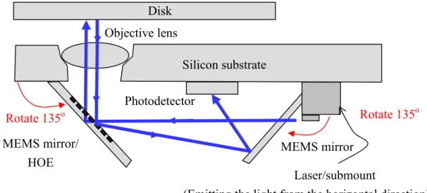
The objective of this research is to fabricate a MEMS-based optical pickup head for blue wavelength. The proposed optical pickup head is composed of a laser diode, a 135o MEMS mirror, a 135o MEMS mirror with holographic optical element (HOE), an objective lens, and a photodetector, as shown in Figure 1-32. Detailed design and principle of the optical system is discussed in Chapter 2. The main components of the optical bench are the two 135o MEMS mirrors. The one-push method in our previous work [22] is used to assemble the 90o and 45o out-of-plane microstructures.
Therefore, the objectives of this thesis include: 1. improving angular accuracy of 45o devices;
2. developing assembling technique for 135o mirrors;
3. assembly of laser diode, photodetector, and objective lens on the fabricated optical bench;
Figure 1-32 Schematic of the MEMS-based optical pickup head in this thesis.
The basic principles and simulation of the proposed optical pickup head and assembly method are presented in Chapter 2. The fabrication processes and process issues are discussed in Chapter 3. The experiment and measurement results are presented in Chapter 4. Conclusion and future work are discussed in Chapter 5.
MEMS mirror/ HOE Photodetector Objective lens Silicon substrate MEMS mirror Rotate 135o Rotate 135o Laser/submount
(Emitting the light from the horizontal direction) Disk
Chapter 2 Principle and Design
2-1 Introduction
A novel MOEMS platform employing SOI wafers and simple push operation as the assembly method is proposed to fabricate the optical bench. The simple push operation was demonstrated in our previous study [22]. It has large probe positioning tolerance in both vertical and lateral directions. In this platform, torsional beams are used to replace micro hinges in assembled structures. Nonvertical micromirrors are developed since the optical system has two 135o mirrors. The optical bench is an optical pickup head for blue-wavelength. The principles of the assembly method and the optical system are discussed in this chapter. Micromirrors with arbitrary angles assembled by using the simple push operation are used to verify the proposed assembly technique.
2-2 Mirror with arbitrary angles
In this section, micromirrors with four different angles are used to verify the methods of assembling of mirrors with arbitrary angles. The 30o, 45o, and 60o micromirrors are assembled by two push operations. 135o mirrors are assembled with a different assembly process. In our previous demonstration [22], the average angle of the assembled 45o micromirrors was 45.89°±0.2°. The cause and solution of this problem are investigated in this thesis.
2-2-1 30o, 45o , and 60o mirrors
The assembly method and design principle of these three mirrors are the same. Therefore, 45o devices are used to illustrate the design principle and assembly process.
The mirror and support are built by using only the device layer of the SOI wafer, whereas the substrate provides the space for pushing. The sizes of the mirror plate and the push pad are (760 μm)2 and (250 μm)2, respectively.
(a) (b)
Figure 2-1 (a) Layout design of the 45o device, (b) 3-D model.
The assembly process of the 45o device is shown in Figure 2-2. Two push operations are needed in the assembly process. First, Probe 1 pushes the support to over 60o and hold in this position (Figure 2-2 (a)). Then Probe 2 pushes the mirror plate to 40o to 50o (Figure 2-2 (b)). Subsequently Probe 1 is removed and the torque from the torsional beams drives the support to lie on the mirror plate (Figure 2-2 (c)). After Probe 2 is removed, the torque of the torsional beams connected to the mirror plate also drives the mirror plate to lie on the support. Finally, the support and the mirror plate are interlocked (Figure 2-2 (d)).
Mirror plate Torsional beams
Mechanical stop Support
Angular positioning interlock
Substrate
Mirror 657 um
657 um 930 um
Figure 2-2 Assembly process of the 45o device.
The layout views of the 30o and 60o mirrors are shown in Figure 2-3. The design principle and assembly process is the same as the 45o mirrors. The sizes of mirror plates are (760 μm)2 and (250 μm)2, respectively.
(a) (b) Figure 2-3 Layout design of (a) 60o device, (b) 30o device.
460 um 805μm 460μm 1065μm 805μm (a) (b) (c) (d) Probe 1 Probe 2 Interlock Mirror Support Torsional beams 1065μm
Torsional beams
For a 45° mirror, the twist angle of the torsional beams is 45°. However, during the assembly process the support is pushed by more than 80°. Thus a twist angle of 80° is assembled in this design. Torsional beams are provide the restoring force and the design is based on the torsional formula of a beam with a rectangular cross section [23], TL KG θ = , (2-1) 4 3 4 16 [ 3.36 (1 )], for > 3 12 b b K ab a b a a = − − , (2-2) 2 3 4 max 2 3 [1 0.6095 0.8865( ) 1.8023( ) 0.9100( ) ], for 8 T b b b b a b ab a a a a τ = + + − + ≥ , (2-3)
where θ is the angle of twist, T is the applied torque, L is the beam length, K is a constant depending on the geometry of beam, G is the shear modulus, τmax is the maximum shear stress at the midpoint of the longer side between a and b, a and b are the half of the longer and shorter sides of the cross section of the beam, respectively (Figure 2-4).
Figure 2-4 Form and dimensions of cross sections.
The device layer of the SOI wafer is 5 μm thick and therefore b is 2.5 μm. The width of the beam is 20 μm and therefore a is 10 μm. The shear modulus of single-crystal silicon is 79.9 GPa [24] and the yield stress of single-crystal silicon is 7 GPa [25]. The maximum shear stress in these structures at θ =80o must be smaller than the yield strength, therefore τmax = 2 GPa is used in this design for a safety factor of 3.5. By substituting these values into Equations 2-1, 2-2, and 2-3, K and T are
2b 2a
24
702.13 10× − m4 and 281.73 10× −9 N⋅m, respectively. From Equation 2-1, L can be found to be 398 μm.
Support rigidity
Support arms are used to lock the mirror plate and apply an opposite torque to lock the mirror plate. The structural strength of the support arms is related to the bending of support arms after the assembly process. When the device is in static equilibrium after assembly, the restoring moment M0 from the torsional beam is applied on the support arm, as shown in Figure 2-5. Therefore, the bending of the support arms is related to the moment from the torsional beams and the rigidity of the support arms. The curvature of the bending support arm can be calculated from
0 EI M ρ = − (2-4) 3 1 12 I = WH (2-5) where E is the Young’s modulus, I is the moment of inertia depending on the geometry of the support arms, Mo is the moment acting on the support after the mirror is assembled. Young’s modulus of silicon is 169 GPa. M0 is equal to T in Equation 2-1. The geometry of torsional beams is 700 μm (L) × 20 μm (W) × 5 μm (H) in our design. By substituting these values into Equation 2-1 and 2-2, M0 is 62.94 10× −9 N⋅m. The angle deviation from the bent support can be calculated, as shown in Figure 2-6. The radius of curvature can be calculated from Equations 2-4 and 2-5. Three different width of support arm with same length l is 657 μm are designed in this thesis. The angular deviation can be calculated from Figure 2-6. Table 2-1 show the calculation results of radius of curvature and the angle deviation with the same geometry of torsional beams (700 μm (L) × 20 μm (W) × 5 μm (H))in the reality design.
Table 2-1 Calculation of angular deviation.
Support arm width 120 μm 250 μm 350 μm
Radius of curvature of bent support 6.71 mm 13.99 mm 19.58 mm
Angular deviation 0.23° 0.11° 0.08°
Figure 2-5 Schematic of static equilibrium after assembly.
Figure 2-6 Schematic of assembled 45° mirror with bent support.
2 l θ ρ Δ = θ Δ ρ l Bent support θ Δ M0 M0
2-2-2 135o mirror
The 135o mirror is composed of a mirror plate and support arms with torsional beams, as shown in Figure 2-7. The geometry of the torsional beam is 1200 μm (L) × 20 μm (W) × 5 μm (H) in our design. The design principle of the torsional beam is the same as that of the 45o mirror. The maximum shear stress in the 135o structures at angle of twist θ =150o must be smaller than 2 GPa. According to the calculation, the length must be lager than 846 μm when the width and height are 20 μm and 5 μm, respectively. The reflective surface is the front side of the device layer, so it can be used to fabricate other reflective optical devices by patterning the device layer of SOI wafer. The fabrication process of the 135o structure is the same as the 30o, 45o, and 60o devices but the assembly process is different.
(a) (b) Figure 2-7 (a) Layout design of 135o device, (b) 3-D model.
The assembly process of the 135o device is shown in Figure 2-8. Two probes are needed in the assembly process. First Probe 1 pushes the mirror plate to about 70o to 90o (Figure 2-8 (a)). Then Probe 2 holds the mirror plate from the back. After the mirror plate is held by Probe 2, Probe 1 is moved from the mirror plate to the push
Substrate
Mirror
Support Torsional beams
Mirror plate
Push pads Angular positioning interlock
657 μm 657 μm
(Figure 2-8 (c)) and Probe 2 pushes the mirror plate forward to 140o to 150o (Figure 2-8 (d)). Subsequently Probe 1 is removed and the torque from the torsional beams drives the support to lie on the mirror plate (Figure 2-8 (e)). Finally, Probe 2 is removed and the mirror is interlocked by the restoring torque from the mirror plate (Figure 2-8 (f)).
Figure 2-8 Assembly process of the 135o device.
(a) (b) (c) (d) (e) (f) Probe 1 Probe 1 Probe 2 Probe 2 Probe 1 Probe 2 Probe 1 Probe 2
2-3 Optical bench and MEMS-based optical pickup head
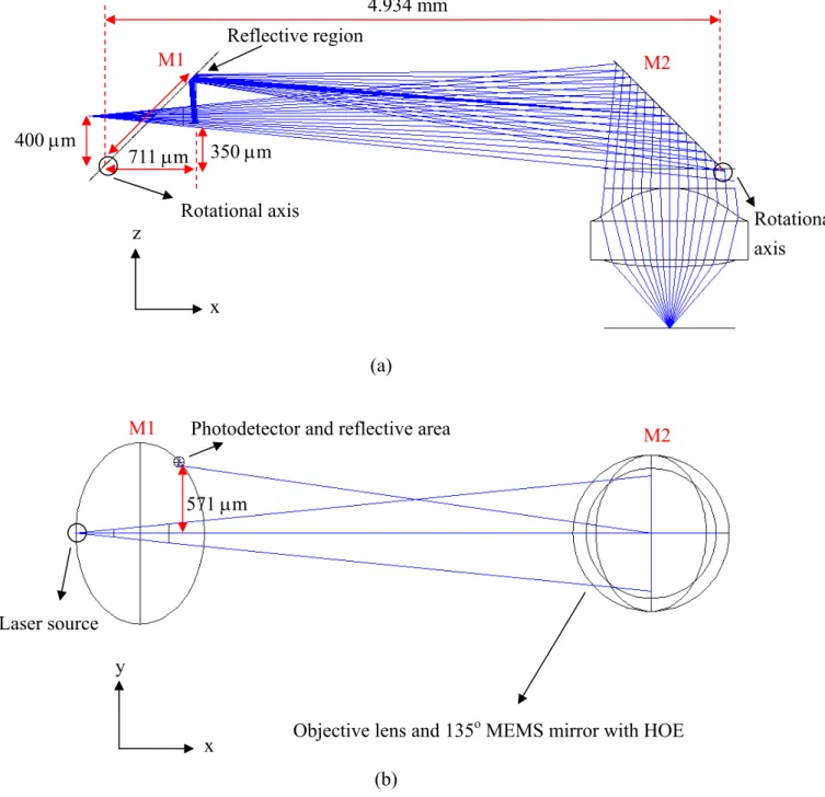
The 135o mirror discussed in the previous section is used in an optical bench for a MEMS-based optical pickup head, as shown in Figure 2-9. The optical pickup head is composed of a laser diode, a 135o MEMS mirror, a 135o MEMS mirror with a holographic optical element (HOE) on the reflective surface, an objective lens, and a photodetector. The light emitted from the laser diode is reflected from the parallel to the vertical direction with respect to the disk surface by the 135o MEMS mirror with holographic optical element (HOE) on the surface. The zeroth-order light reflected by the 135o MEMS mirror with HOE is focused on the disk. On the returning path, the first-order light diffracted by the HOE is reflected by another 135o MEMS mirror, and finally projected onto the photodetector. The focusing error signal (FES) can be generated from the HOE diffraction. The simulation of the optical system is discussed below.
Figure 2-9 Schematic of the MEMS-based optical pickup head. MEMS mirror/ HOE Photodetector MEMS mirror Rotate 135o Rotate 135o Silicon substrate Holder Objective lens Laser/submount Disk
2-3-1 Simulation of the MEMS-based optical pickup head
Figure 2-10 shows the simulation of the optical pickup head system by Zemax. The wavelength of laser source is 405 nm. The numerical aperture (NA) of the objective lens is 0.65, the focal length is 0.67 mm, and the working distance of is 0.47 mm. The optical spot in forward optical path on the disk can be optimized by ZEMAX so that its size is smaller than the diffraction limit, as shown in Figure 2-11.
Figure 2-10 Zemax simulation of the MEMS-based optical pickup head.
Figure 2-11 Zemax simulated optical spot on the disk.
Laser diode 135o mirror Objective Lens Photo detector Disk 135o mirror/ HOE
Holographic optical element [26]
On the returning optical path, the first-order light is diffracted by the astigmatic focusing holographic optical element (HOE) and the light is reflected onto the photodetector by another 135o MEMS mirror. The HOE pattern can be designed as a phase-type binary optical element with the phase polynomial represented by
0 0 ( , ) M N m n mn m n x y C x y φ = = =
∑∑
(2-6) The design of the HOE phase polynomial is similar to [26]. In the current optical pickup head system,2 2 3 2 2 3 ( , ) 2197 705 96.64989 524.26125 27.601696 64.301924 24.624489 45.460183 0.324068 x y x y x xy y x x y xy y φ = − + + + − + − − + (2-7)
where the x term and y term represent the diffraction angle in the x-direction and y-direction, respectively. The x2 term, xy term, and y2 term are related to the focus and astigmatism of the beam; the x2 term and y2 term represent the focusing capability in the x-direction and y-direction, respectively. The other higher order terms are used for correcting the spherical aberration, coma, and high-order aberrations. By designing these terms of the phase polynomial properly, the optical spot projected on the photodetector will change sharp depending on whether the optical path is in focus or out of focus. Figure 2-12 shows the optical spot on the photodetector when the optical path has a defocus from -10 um to +10 um. Astigmatic aberration can be observed in the diffracted out-of-focus spots.
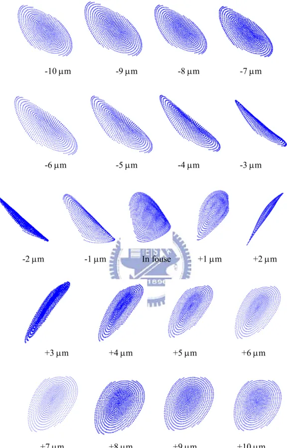
-10 μm -9 μm -8 μm -7 μm -6 μm -5 μm -4 μm -3 μm -2 μm -1 μm In fouse +1 μm +2 μm +3 μm +4 μm +5 μm +6 μm +7 μm +8 μm +9 μm +10 μm
Figure 2-12 Simulated optical spot on the photodetector with various amount of defocus.
S-curve
In order to read the information on the disk, the optical spot must be focused on the disk accurately. Therefore, focusing servo control is necessary in optical pickup head system. The focusing error signals can be generated from photodetector and used as feedback signals to the actuator. The actuator can keep the system in focus by changing the position of the objective lens. Figure 2-13 shows the schematic of the astigmatic method for generating the focus error signal. Figure 2-12 (a) shows optical spot projected onto the quad photodetector when the system is in focus. The size of a photodetector element is (47.5 μm)2. Figures 2-13 (b) and (c) show the optical spot projected onto the quad photodetector when the system is defocused in opposite directions. The focusing error signal can be calculated from the light intensity on the photodetectors by using Equation 2-8.
FES= (A+C)-(B+D). (2-8) When the optical spot is in focus on the disk, the light intensity on each photodetector is equal (A=B=C=D) and the FES is zero (Figure 2-13 (a)). But when the optical spot is not in focus, the light intensity on the photodetector is not equal and the FES is either positive or negative (Figure 2-13 (b), (c)). The relation between the FES and the defocus distance is the S-curve of this optical pickup head system. Figure 2-14 shows the simulation result of the S-curve in this system. The linear region of the FES is about 5 μm.
(a) (b) (c) Figure 2-13 Schematic of the astigmatic method.
Figure 2-14 Simulation of the S-curve.
2-3-2 Diffractive efficiency of HOE
On the forward path, the zeroth-order light reflected from the HOE is focused on the disk. On the returning path, the first-order light diffracted by the HOE is reflected by another 135o MEMS mirror and finally projected on the photodetector. The light intensity is reduced due to the reflection and diffraction. Since the power loss due to reflection is much smaller than that due to diffraction, only the diffraction efficiency of the HOE is discussed in this section.
Linear region A B C D A B C D A B C D FES= (A+C)-(B+D) 50 μm 5 μm
Figure 2-15 shows the schematic of the light wave passing through a diffractive optical element. In the scalar diffraction theory, the incident distribution of optical field on the diffractive optical element can be expressed as
( , )
0( , ) ( , )
i u v
g u v = A u v eφ (2-9) where u and v represent the position on the diffractive optical element, A and φ represent the amplitude and phase functions, respectively. After the light wave passes through the diffractive optical element, the distribution of the optical field is modified as
( , )
( , ) ( , ) i u v ( , )
g u v =A u v eφ t u v (2-10) where t represents the transmission function and can be expressed as
'( , )
( , ) '( , ) i u v
t u v =A u v eφ (2-11) The distribution of the optical field on the image plane can be express as Equation 2-12 from the Huygens-Fresnel principle [27]
2 ( , ) z ( , )eikr U U u v dudv i r ζ η λ ∑ =
∫∫
(2-12) where z is the distance between the diffractive optical element and the image plane. Equation 2-12 can be reduced to Equation 2-13 by the Fraunhofer approximation when z is larger than the area of diffractive optical element. It is also called the far-field diffraction. 2 2 ( ) ( 2 ) 2 ( ) ( , ) ( , ) u v ik z z i u v z e U U u v e dudv i z π ζ η λ ζ η λ + + ∞ − + −∞ =∫ ∫
(2-13)From Equation 2-13, the distribution of the optical field on the ( , )ζ η plane is the
Figure 2-15 Schematic of diffraction theory.
Figure 2-16 shows the schematic and phase distribution of the reflective linear phase grating. The depth and the period of the grating are d and T, respectively. The light wave is perpendicularly incident on the grating and then reflected to the image plane. The optical path difference of this grating is equal to 2d (Figure 2-16 (a)). Therefore, the transmission function of the grating can be expressed as Equation 2-14 (Figure 2-16 (b)), where φ represent the phase difference and can be expressed as a function of the optical path difference, as shown in Equation 2-15.
1 2 2 ( ) 2 2 1 2 2 i T S x S S f x e x S T x φ ⎧ − < < ⎪ ⎪ ⎪ =⎨ − < < ⎪ ⎪ < < ⎪⎩ (2-14) 2π φ λ
= ⋅(optical path difference) (2-15)
Image plane Diffractive optical element u g(u,v) g0(u,v) G( , )ζ η η v Z z ζ
Figure 2-16 (a) Schematic and (b) phase distribution of the reflective linear phase grating.
As in the scalar diffraction theory discussed above, the diffraction efficiency of the linear grating can be calculated by Fourier transform. In our design, the efficiency of the HOE can be calculated as a reflective phase grating. Since the HOE is patterned on the 135o mirror, the optical path difference is 2 2d in our design, as shown in Figure 2-17. When the optical path difference 2 2d is substituted in Equation 2-15, the diffraction efficiency of this system can be calculated by the Fourier transform of
( )
f x in Equation 2-14. Because of the periodicity, the transmission function can be expanded as a Fourier series. The Fourier coefficients am and bm give the values of the
amplitudes in each diffraction orders. First-order and zeroth-order beams are used in our design, so only a0, a1, b1 are calculated below.
d (a) (b) 1 i eφ T d S λ=405 nm
Figure 2-17 Schematic of the reflective type linear phase grating on 135o mirror. 0 1 1 2 2 ( ) cos( ) cos( ) 2 m m m m a mx mx f x a b T T π π ∞ ∞ = = = +
∑
+∑
/2 /2 /2 /2 0 /2 /2 /2 /2 1 1 ( ) [ 1 1 ] 1 T S S j T T T S S j a f x dx dx e dx dx T T S S e T T φ φ − − − − = = + + = − + ⋅∫
∫
∫
∫
/2 /2 /2 /2 /2 /2 /2 /2 1 2 1 2 2 2( ) cos [ cos cos cos ]
[2sin 2sin 2 sin ]
2 T S S j T m T T S S j m x m x m x m x a f x dx dx e dx dx T T T T T T T m S m S m e m T T φ φ π π π π π π π π − − − − = = + + = − + ⋅
∫
∫
∫
∫
/2 /2 /2 /2 /2 /2 /2 /2 1 2 1 2 2 2( )sin [ sin sin sin ]
0 T S S j T m T T S S m x m x m x m x b f x dx dx e dx dx T T T T T T φ π − π π π − − − = = + + =
∫
∫
∫
∫
Because the duty cycle of the HOE is 0.5 in our design, S/T=0.5 and
0 1 0 1 0.5( 1) 1 ( 1) 0.5( 1) 0 j j j a e a e a e b φ φ φ π ⎧ = + ⎪ ⎪ = − = + ⎨ ⎪ = ⎪⎩ (2-16) d 45o λ=405 nm
The coefficients a0, a1, b1 represent the amplitude of the zeroth-order and first-order beams, respectively. The intensity of light is equal to the square of the amplitude, so the diffraction efficiency of the zeroth-order and first-order light can be calculated as
2 4 2 2 0 0 1 (1 ) 2 j d a e π λ η = = + 2 2 4 2 2 1 1 1 1 ( 1) ( 1) j d j a e e π φ λ η π π = = − = − (2-17)
Figure 2-18 shows the calculated diffraction efficiency. Because the optical pickup head uses zeroth-order diffraction on the forward path and first-order diffraction on the return path, the total efficiency is equal to the product of the two efficiencies, as shown in Figure 2-18. Therefore, to get the maximum power on the photodetector, the optimum etching depth of the HOE is odd multiples of 36.2 nm.
0 50 100 150 200 250 300 350 400 450 500 0 0.1 0.2 0.3 0.4 0.5 0.6 0.7 0.8 0.9 1 Etch depth (nm) D iff ra ct ion ef fic ienc y
HOE efficiency for 405nm
zero order (405nm) first order (405nm) zero * first (405nm)
2-3-3 Layout design
In the layout of the optical bench, the positions of the components, including the photodetector, the objective lens, the laser source, the distance between two 135o MEMS mirror, and the reflective area on the 135o MEMS mirror without HOE, must match the optical system in the simulation. The HOE pattern is generated by the phase polynomial. The layout design of the optical bench is discussed in this section.
HOE pattern
The pattern of the HOE is shown in Figure 2-19. The pattern is generated by the phase polynomial in Equation 2-6. The duty cycle and width of the HOE are 0.5 and 1.3 μm (1.36 μm × cos 17.8 o), respectively. The pattern of the HOE has an angle of 72.2o, as can be calculated from the phase polynomial shown in Equation 2-7. The x term and y term represent the diffraction direction in the x-direction and y-direction, respectively. So the diffraction direction of the HOE is
1 coefficient of the tern 1 705
tan ( ) tan ( )
coefficient of the tern 2197
y x
θ = − = − = 17.8o (2-18)
where the 705 and 2197 are the coefficients of the x term and y term from Equation 2-7. In order to realize the astigmatic method for focusing error signals, the diffracted optical spot must be projected to the center of the quad photodetector elements. The diffraction direction of 17.8o is designed to match this condition. Therefore, the HOE is patterned at the complement angle of the diffraction direction of 72.2o.
Figure 2-19 Layout of the holographic optical element.
Optical path
Figure 2-20 shows the schematic of the optical bench after assembly. Figure 2-21 shows the side-view and top-view of the optical path. The distance between the rotation axes of the two 135o MEMS mirror is 4934 μm. The center of the quad photodetector has a distance of 711 μm from the rotational axis of M1 in the x-direction and a distance of 571 μm from the optical axis of the forward path in the y-direction. The reflective region of M1 in Figure 2-21 (a) has a distance of 991 μm from the rotational axis in the x-direction before the 135o mirror is assembled. Finally, the completed layout of optical bench is shown in Figure 2-22. The tolerance of the 135o devices are simulated as 1o [28].
Figure 2-20 Schematic of the optical bench after assembly. 1.36 μm
1.3 μm
M1 M2
Laser diode photodetector
Optical path
(a)
(b)
Figure 2-21 Optical simulation of the system, (a) side-view, (b) top-view. Rotational axis x z M1 M2 350 μm 711 μm Reflective region 571 μm
Photodetector and reflective area
x y
Objective lens and 135o MEMS mirror with HOE
M1 M2 Rotational axis 400 μm Laser source 4.934 mm
Figure 2-22 Layout of optical bench.
2-4 Summary
Mirrors with four different angles are designed to demonstrate the assembly method for arbitary angles. Different dimensions of torsional beams and locking mechanism are used to test the angular positioning accuracy. The optical bench is designed to realize the optical pickup head. In Chapter 3, the fabrication is discussed.
Laser source 4.934 mm
Rotational axis Rotational axis
Photo detector (1mm x 1mm)
Si3N4 layer and pad
Si3N4 layer and pad
Reflective area (300um x 300um) Objective lens (ψ= 1200 um) 911 um 571 um 1241 um 1241 um 1756 um 1571 um 1571 um 2221 um PT-HOE (1600 um x 1600 um)
![Figure 1-3 Waveguide type optical pickup head, (a) fabrication process, (b) schematic [2]](https://thumb-ap.123doks.com/thumbv2/9libinfo/7903462.156082/17.892.139.745.773.1060/figure-waveguide-type-optical-pickup-fabrication-process-schematic.webp)
![Figure 1-10 SEM of a free-rotating hinged micromirror lifted by an array of SDA [9].](https://thumb-ap.123doks.com/thumbv2/9libinfo/7903462.156082/23.892.245.683.397.721/figure-sem-free-rotating-hinged-micromirror-lifted-array.webp)
![Figure 1-16 Step-by-step photographs of the four-step sequential assembly [12].](https://thumb-ap.123doks.com/thumbv2/9libinfo/7903462.156082/27.892.160.757.109.372/figure-step-step-photographs-step-sequential-assembly.webp)
![Figure 1-18 Batch assembly by centrifugal force: (a) an array of bridge structures, (b) an array of micromirrors [13]](https://thumb-ap.123doks.com/thumbv2/9libinfo/7903462.156082/28.892.147.735.752.1024/figure-batch-assembly-centrifugal-force-bridge-structures-micromirrors.webp)
![Figure 2-17 Schematic of the reflective type linear phase grating on 135 o mirror. 0 1 12 2( )cos()cos( )2mmmmamxmxf xabTTππ∞∞===+∑+∑ /2 /2 /2 /2 0 /2 /2 /2 /211( )[1 1 ] 1 T S S j TTTSSjaf x dxdxe dx dxTTSSe T T φφ−−−−==+ += − + ⋅∫∫∫ ∫ /2 /2 /2 /2 /](https://thumb-ap.123doks.com/thumbv2/9libinfo/7903462.156082/57.892.268.566.108.463/figure-schematic-reflective-grating-mmmmamxmxf-xabttππ-tttssjaf-dxttsse.webp)