IEEE ELECTRON DEVICE LETTERS, VOL. 26, NO. 11, NOVEMBER 2005 811
A Source-Follower Type Analog Buffer Using
Poly-Si TFTs With Large Design Windows
Ya-Hsiang Tai, Cheng-Chiu Pai, Bo-Ting Chen, and Huang-Chung Cheng
Abstract—New simple source follower circuits using low-temper-ature polycrystalline silicon thin-film transistors (LTPS-TFTs) as analog buffers for the integrated data driver circuit of active-ma-trix liquid crystal displays and active-maactive-ma-trix light emitting diodes are discussed. In addition to the threshold voltage difference of driving TFTs, the unsaturated of output voltage arisen from the significant subthreshold current will also result in the difficulty of the buffer circuit design. The proposed circuit is capable of min-imizing the variation from both the signal timing and the device characteristics.
Index Terms—Active-matrix light emitting diodes (AMOLEDs), active-matrix liquid crystal displays (AMLCDs), low-temperature polycrystalline silicon thin-film transistors (LTPS-TFTs) , source follower.
I. INTRODUCTION
L
OW-temperature poly-Si thin-film transistors (LTPS-TFTs) have attracted much attention in the application on the integrated peripheral circuits of active-matrix liquid crystal displays (AMLCDs) and active-matrix light emitting diodes (AMOLEDs) [1]–[3]. In a poly-Si TFT-LCD, poly-Si TFT is used to implement pixel circuit and driving circuit on a single glass substrate to reduce system cost and possess compact module.Among the many driving circuits employing LTPS TFTs, the output buffer is indispensable to drive the large load capacitance of the data bus. There are several requirements for the output buffer for a flat-panel display column driver [4]. For example, as resolution gets higher, more analog buffers are needed. There-fore, its layout area must be reduced. In addition, power dissipa-tion must be minimized while displays are used toward portable applications. However, compared to the MOSFETs, LTPS TFTs suffer from poor electrical characteristics and huge variations. It will cause the real output voltage to not achieve the target value and lead to the wrong gray scale. Thus, the output devia-tion must be decreased as possible.
Manuscript received July 21, 2005; revised August 15, 2005. This work has been sponsored National Science Council, Taiwan, R.O.C., under Grant 93-2215-E-009-075 and the Ministry of Education of Taiwan, R.O.C., the Program for Promoting Academic Excellent of Universities under Grant 1-E-FA04-2-4-B. The review of this letter was arranged by Editor J. Sin.
Y.-H. Tai is with the Department of Photonics and Display Institute, National Chiao-Tung University, Hsinchu 300, Taiwan, R.O.C. (e-mail: [email protected]).
C.-C. Pai is with the Department of Photonics and Institute of Electro-Optical Engineering, National Chiao-Tung University, Hsinchu 300, Taiwan, R.O.C.
B.-T. Chen and H.-C. Cheng are with the Department of Electronics Engi-neering and Institute of Electronics, National Chiao-Tung University, Hsinchu 300, Taiwan, R.O.C.
Digital Object Identifier 10.1109/LED.2005.857689
Fig. 1. Conventional source follower and output waveform simulation results.
Among these output buffer circuit for displays, source fol-lower is considered an excellent candidate for the system on panel (SoP) application [5]–[10].
II. UNSATURATEDPHENOMENON OF THEOUTPUTVOLTAGE
The typical model of the LTPS TFTs used in this paper is represented by the Rensselaer Polytechnic Institue parameters. In this letter, the charging time is about 50 s and the data line loading capacitance is assumed 20 pF corresponding to a 2-in quarter video graphics array LCD. A conventional source fol-lower and its output waveform are shown in Fig. 1. It is observed that the final output voltage is not kept constant, but exceeds the value of expected in principle. It is ascribed to the sub-threshold current. As model used in this work, the subsub-threshold swing of LTPS TFTs is about 0.3 V/dec that is much larger than MOSFETs’ (0.06 V/dec). Consequently, it will be sensitive to the charging time for various product specifications. An active load is added to eliminate this phenomenon and simulation re-sult is also shown in Fig. 2. It is distinct that unsaturated phe-nomenon of the output voltage is suppressed. Fig. 3 plots the offset voltage ( ) versus input voltage ( ) of con-ventional source follower and source follower with active load in different charging time. It is observed that the offset voltage of conventional source follower and source follower with ac-tive load varies with different input voltage. The offset voltage difference of conventional source follower is larger than source follower with active load with different charging time. Although offset voltage of source follower with active load larger than conventional source follower, it can be eliminated by gamma correction [8], [11]. Therefore, the charging time variation-tol-erant characteristic of source follower with active load is supe-rior to the conventional source follower.
812 IEEE ELECTRON DEVICE LETTERS, VOL. 26, NO. 11, NOVEMBER 2005
Fig. 2. Conventional source follower with an active load and output waveform simulation results.
Fig. 3. Comparison of conventional source follower and source follower with an active load in various charging time.
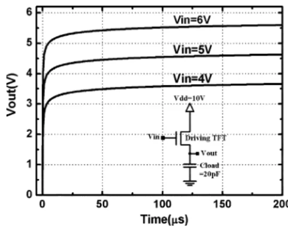
Fig. 4. Simulation results of the conventional source follower with an active load when input voltage 4 to 6 V.
III. DISTRIBUTEDPHENOMENON OF THEOUTPUTVOLTAGE
To study the effect of the device variation on circuit perfor-mance, Monte Carlo simulation with an assumption of normal distribution is executed where the mean value and the deviation of the threshold voltage and mobility are 1 and 0.5 V, and 77.1 and 15 cm , respectively. Each of the TFTs in the circuit varies independently.
Fig. 4 shows the simulation results of the conventional source follower with active load when input voltage are 4 and 6 V. It
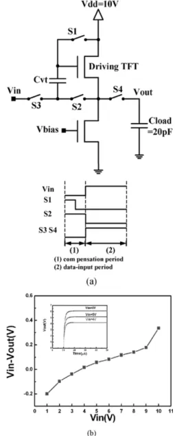
Fig. 5. (a) Proposed analog buffer and its timing diagram. (b) Simulation results of the proposed analog buffer when input voltage ranges from 1 to 10 V and the inset shows the Monte Carlo simulation results when input voltage 4 to 6 V.
is clear that the circuit suffers from huge variations and output voltage is not due to the LTPS TFTs variation. There-fore, a new analog buffer is proposed in this paper for the com-pensation of the device variation.
Fig. 5(a) shows a schematic of the proposed analog buffer consisting of two transistors, a capacitor, and four switches. The gate voltage of the TFT as the active load is biased at . The driving schemes are as follows. During the first operating period, S1 and S2 are turned on sequentially, and S3 and S4 are turned off. Thus, a voltage corresponding to the threshold voltage of driving TFT, the threshold voltage of the active load and the bias voltage is stored in . After sampling period, S3 and S4 are turned on and S1 and S2 are turned off, then the voltage at the gate of the driving TFT is hold. Thus, the output voltage is compensated by the voltage stored in . These re-sults can be expressed as follows: (We assumed that the driving TFT as TFT1 and the active load as TFT2)
TAI et al.: SOURCE-FOLLOWER TYPE ANALOG BUFFER USING POLY-Si TFTs 813
(1) Compensation period
(2) Data-input period
The formula indicates that the variation of driving TFT and the active load can be stored for the compensation during the com-pensation period.
Fig. 5(b) shows the offset voltage ( ) versus input voltage ( ) of proposed source follower and the inset shows the Monte Carlo simulation results when input voltage 4 to 6 V. The output voltage variation also decreases drastically com-pared with Fig. 4.
IV. CONCLUSION
A novel source follower has been proposed, where the driving circuit is formed by only two n-type thin film transistors, a ca-pacitor, and four switches. Much improved output voltage sta-bility and simple configuration are achieved by adding the bias
circuit and the compensation operation. The proposed source follower is capable of minimizing the variations from signal timing and the device characteristics.
ACKNOWLEDGMENT
The authors would like to thank the Toppoly Optoelectronics Corporation for their technical support.
REFERENCES
[1] H. G. Yang, S. Fluxman, C. Reita, and P. Migliorato, “Design, measure-ment and analysis of CMOS polysilicon TFT operational amplifiers,”
IEEE J. Solid-State Circuits, vol. 29, no. 6, pp. 727–732, Jun. 1994.
[2] T. Matsuo and T. Muramatsu, “CG silicon technology and development of system on panel,” in SID Tech. Dig., 2004, pp. 856–859.
[3] Y. Matsueda, R. Kakkad, Y. S. Park, H. H. Yoon, W. P. Lee, J. B. Koo, and H. K. Chung, “2.5-in AMOLED with integrated 6-bit gamma com-pensated digital data driver,” in SID Tech. Dig., 2004, pp. 1116–1119. [4] P. C. Yu and J. C. Wu, “A class-B output buffer for flat-panel-display
column driver,” IEEE J. Solid-State Circuits, vol. 34, no. 1, pp. 116–119, Jan. 1999.
[5] S. H. Jung, C. W. Han, I. H. Song, and M. K. Han, “A new poly-Si analog buffer using source follower for active matrix displays,” in Proc.
International Display Workshop, 2003, pp. 1683–1684.
[6] H. J. Chung, S. W. Lee, and C. H. Han, “Poly-Si TFT push-pull analogue buffer for integrated data drivers of poly-Si TFT-LCDs,” Electron. Lett., vol. 37, no. 17, 2001.
[7] Y.-S. Yoo, J.-Y. Choi, H.-S. Shim, and O.-K. Kwon, “A high accurate analog buffer circuit using low temperature poly-Si TFT,” in SID Tech.
Dig., 2004, pp. 1460–1463.
[8] S.-H. Jung, J.-H. Park, C.-W. Han, and M.-K. Han, “New source follower type analog buffers using poly-Si TFTs for active matrix displays,” in
SID Tech. Dig., 2004, pp. 1452–1455.
[9] M. Lee and I. Lee, “Reducing the poly-Si TFT nonuniformity by tran-sistor slicing,” J. Inf. Display, vol. 2, no. 2, Jun. 2001.
[10] Y. Kida, Y. Nakajima, M. Takatoku, M. Minegishi, S. Nakamura, Y. Maki, and T. Maekawa, “A 3.8 inch half-VGA transflective color TFT-LCD with completely integrated 6-bit RGB parallel interface drivers,” in Proc. Eurodisplay, 2002, p. 358.
[11] H. Kageyama, H. Akimoto, Y. Shimizu, T. Ouchi, N. Kasai, H. Awakura, N. Tokuda, K. Kajiyama, and T. Sato, “A 2.5-inch OLED display with a three-TFT pixel circuit for clamped inverter driving,” in SID Tech. Dig., 2004, pp. 1394–1397.