國
立
交
通
大
學
電信工程學系碩士班
碩
士
論
文
以電流再利用之 CMOS 射頻前端關鍵元件設計
The key components of CMOS RF front-end with
current-reused approach
研 究 生:黃智偉
指導教授:鍾世忠 教授
吳霖堃 教授
以電流再利用之 CMOS 射頻前端關鍵元件設計 The key components of CMOS RF front-end
with
current-reused approach
研 究 生:黃智偉 Student:Chih-Wei Huang 指導教授:鍾世忠 教授 Advisor:Dr. Shyh-Jong Chung 吳霖堃 教授 Dr. Lin-Kun Wu
國 立 交 通 大 學 電 信 工 程 系
碩 士 論 文
A Thesis
Submitted to Department of Computer and Information Science College of Electrical Engineering and Computer Science
National Chiao Tung University in partial Fulfillment of the Requirements
for the Degree of Master
in
Communication Engineering June 2008
Acknowledgements 在這兩年的研究所生涯中,非常地感謝指導教授鐘世忠老師和吳 霖堃老師,能夠讓我有這個機會進入到實驗室來學習,不只在研究上 能夠受到非常專業及一流的指導,讓自己對於射頻電路設計有著非常 多的體悟和認識,在生活上,身邊的人也都會彼此幫忙和一起玩樂, 處處充滿了溫馨的氣息,對我來說這是一段非常美好和珍貴的回憶。 我還要非常地感謝實驗室的博班學長佩宗、標哥、竣義、阿信非 常地盡心盡力給予相當豐富的經驗和教導,也要感謝畢業的學長姐敦 智、煥能、碰碰、源哥能夠回來提供很好的建議,另外,也很感謝 Useful、威聰能夠常常一起討論和解決問題,還有非常地感謝在 912 辛苦耕耘的學長姊和同學以及學弟妹們,對於自己不熟悉的領域,總 是熱心地給予我很大的幫助和建議,真的非常感謝你們。 最後,我想感謝我的家人,一直不斷地給予我許多的鼓勵和建 議,在你們的陪伴下,讓我能夠順利地完成學業,你們對我的幫助真 的一言難盡。還要感謝我的女友小孟,常常在我最需要的時候幫助 我,不管是在生活上或是心靈上,都對我有莫大的幫助,讓我這兩年 能夠開心地過著生活。最後最後,要謝謝大家在這兩年的教導與陪 伴,不論是一起努力或是一起玩樂,對我來說都是一段非常難忘和快 樂的時光。
以電流再利用之 CMOS 射頻前端關鍵元件設計 學生:黃智偉 指導教授:鍾世忠 博士 吳霖堃 博士 國立交通大學 電信工程研究所碩士班 摘要 本論文分為具帶拒濾波之低雜訊放大器和具內建震盪器之低功 率混頻器兩個部分。利用標準 TSMC 0.18 um RF CMOS 製程完成本論 文中所設計的電路。 第一部分描述設計一個低功率之帶拒濾波低雜訊放大器。其量測 結果之 power gain 在 3~10GHz 內大於 9.5dB,NFmin 為 2.6dB, S11<-5.4dB,不包含緩衝級之功率消耗為 6.8mW,接著使用主動式電 感實現之微小化的帶拒濾波器,使得整體電路之 core area 只有 0.0016 mm2 。其量測之 power gain 為 8~12dB、S11<-11dB、在 2.5GHz 和 5.2GHz 頻段附近抑制干擾訊號的效果分別為 19dB 及 38dB,功率 消耗為 10.3mW,模擬之 NFmin為 2dB、P1dB 為-14.2dB。 第二部分描述震盪器與混頻器之結合與設計。使用電流再利用的 方式達到低功率的效果,並進一歩將平衡非平衡轉換器整合在電路 中,它包含了一個混頻器和震盪器及一個 balun。此整體電路可達功
The key components of CMOS RF front-end with
current-reused approach
student : Chih-Wei Huang Advisors: Dr. Shyh-Jong Chung Dr. Lin-Kun Wu
Institute of communication engineering National Chiao Tung University
ABSTRACT
The thesis consists of three parts: low noise amplifier, LNA with notch filters and low-power oscillator mixer. These propose circuits are fabricated using a standard TSMC 0.18 um RF CMOS process technology.
The first part of the thesis is the low power design of low noise amplifier with notch filters. The measurement result of LNA shows the power gain is more than 9.5dB in 3~10GHz, return loss is under -5.4dB, NFmin is 2.6dB, and power consumption exclude buffer is 6.8 mW. Then,
we use the design of the miniaturized notch filters realized by active inductor, applied in the integration of LNA. The core area of LNA and notch filters is only 0.0016 mm2. The measurement result of LNA with notch filter shows the power gain is 8~12dB, return loss is under -7.5dB. The suppressed performance of notch filters in 2.5GHz and 5.2 GHz are 19dB and 38dB. The power consumption is 10.3 mW. The simulation results of minimum noise figure and P1dB are 2dB and -14.2dB.
The last part describes the combination of VCO and mixer. The circuit uses current-reuse to reach low power consumption, and furthermore a balun is integrated in this design. The total schematic contains mixer, VCO, and on-chip balun. The chip area is 1mmx1.5mm. The simulation results show the conversion gain are 15dB, return loss is under -12dB, P1dB is -16dB. The phase noise is -105 dBc/MHz. The total power consumption is 6mW.
Contents
Chapter 1 Introduction ... 1
1.1 Motivation ... 1
1.2 Thesis Organization ... 2
Chapter 2 General Backgrounds ... 3
2.1 Current-reused Structure ... 3
2.2 The Direct Conversion Receiver ... 6
2.3 The Basic Low Noise Amplifier ... 9
2.3.1 The analysis of transistor noise model [9] ... 9
2.3.2 The basic of low noise amplifier ... 10
2.4 Mixer Fundamentals ... 11 2.4.1 Principles of Mixer ... 11 2.4.2 Performance Parameters ... 12 2.4.2.1 Conversion Gain ... 12 2.4.2.2 Linearity ... 13 2.4.2.3 Isolation ... 15 2.4.3 Mixer Architecture ... 16
2.5 The Review of VCO ... 18
2.5.1 Principles of VCO ... 18
2.5.1.1 LC Tank Voltage-Controlled Oscillator ... 20
2.5.1.2 Ring Oscillator ... 22
2.5.2 Performance Parameters ... 22
2.5.2.1 Phase Noise ... 23
2.5.2.2 Frequency Tuning Range ... 24
2.5.3 Noise Model of VCO ... 25
2.5.3.1 Time Invariant Model ... 25
2.5.3.2 Time Variant Model ... 27
Chapter 3 The Design of LNA with Notch Filters for UWB ... 33
3.1 Circuit Design of the UWB LNA with low power ... 33
3.1.1 Input-matching stage ... 33
3.1.2 Output-matching stage ... 35
3.1.3 Noise analysis ... 36
3.2 The Integration of LNA with Notch Filters ... 38
3.2.1 The design of notch filters with active inductors ... 38
3.2.2 The total design with small area and low power ... 44
3.3 Simulation and Measured Results ... 44
3.3.2 Simulation and Measured Results of LNA with notch
filters ... 47
3.4 Comparison and Summary ... 49
Chapter 4 The Integration of Mixer and VCO with Balun ... 52
4.1 Circuit Design of the Mixer and VCO with Balun ... 52
4.1.1 Analysis of the mixer with current-bleeding method ... 52
4.1.2 The replacement of current source with VCO ... 53
4.1.3 The addition of the balun ... 54
4.1.4 Total design circuit ... 56
4.2 Simulation Results ... 57
4.3 Comparison and Summary ... 62
Chapter 5 Conclusion ... 63
Figures
Fig. 2.1 current-reused quadrature VCO(QVCO) ... 3
Fig. 2.2 Folded-switching mixer with current-reuse ... 4
Fig. 2.3 Circuit schematic of the down-conversion double-balanced ... 5
Fig. 2.4. Block diagram of direct conversion receiver architecture. ... 6
Fig. 2.5. LO signal leakage. ... 8
Fig. 2.6. A strong interferer signal leakage. ... 8
Fig. 2.7. Even order distortion. ... 8
Fig. 2.8. A noise model of MOSFET ... 10
Fig. 2.9 common-source input stage with inductive source degeneration ... 11
Fig. 2.10 P1dB. ... 15
Fig. 2.11 IIP3. ... 15
Fig. 2.12 Passive mixer. ... 16
Fig. 2.13 Active mixer. ... 17
Fig. 2.14 The prototype of the CMOS Gilbert mixer ... 17
Fig. 2.15. Phase noise in receiver. ... 19
Fig. 2.16 Negative resistance and LC tank resistance. ... 20
Fig. 2.17 Series to parallel. ... 20
Fig. 2.18 Equivalent resonant model. ... 20
Fig. 2.19 Input impedance of NMOS cross-coupled pair. ... 21
Fig. 2.20 Complementary cross-coupled pair. ... 22
Fig. 2.21 Ring oscillator. ... 22
Fig. 2.22 Output spectrum of ideal and actual oscillators. ... 23
Fig. 2.23 Lesson’s phase noise model. ... 24
Fig. 2.24 Impulse current injects into LC tank. ... 27
Fig. 2.25 Waveforms for impulse excitation. ... 28
Fig. 2.26 Conversion of noise to phase noise sidebands. ... 31
Fig. 3.1 Schematic of the cascade structure ... 33
Fig. 3.2(a) Schematic with Rf (b) S(1,1) with Rf and without Rf ... 34
Fig. 3.3(a) Schematic with Ls (b) S(1,1) with Ls and without Ls ... 34
Fig. 3.4 Time-domain step current responses in (a) simple RC and (b) shunt peaking inter-stage networks. ... 35
Fig. 3.5 Time-domain step current responses in HS peaking
inter-stage networks. ... 35
Fig. 3.6 the schematic of input-matching and output matching ... 36
Fig. 3.7 (a) Schematic with Rb (b) Improvement of the noise figure ... 37
Fig. 3.8(a)Noise figure with different Rf (b)S(2,1) with different Rf ... 37
Fig. 3.9 S(1,1) with different Rf ... 37
Fig.3.9 The analysis of the Q factor ... 38
Fig.3.10 The filtering ability with increase inductance value .. 39
Fig.3.11 The design of negative resistance ... 39
Fig.3.12 The design of suppressing circuit ... 40
Fig.3.13 The concept of active inductor ... 41
Fig.3.14 The schematic of the active inductor ... 41
Fig.3.15 Active inductor with additional Rf ... 42
Fig.3.16 Using M3 to improve the Q factor ... 42
Fig.3.17 The final improved active inductor ... 42
Fig.3.18 The basic concept of suppressing WiFi signals ... 43
Fig.3.19 The concept diagram of suppressing circuit and simulation result ... 43
Fig.3.21 The magnitude of S11 and S21 ... 45
Fig.3.22 The magnitude of P1dB ... 46
Fig. 3.23 The Noise Figure ... 46
Fig.3.24 The magnitude of S11 and S21 for LNA with notch filters ... 48
Fig. 3.25 The Noise Figure of LNA with notch filters ... 48
Fig. 4.1 Gilbert-type mixer with current bleeding circuits ... 53
Fig. 4.2 Replace current bleeding circuits with VCO ... 54
Fig. 4.3 The schematic of the proposed balun ... 55
Fig. 4.4 The simulation s-parameters of proposed balun ... 55
Fig. 4.5 The simulation phase difference of proposed balun ... 56
Fig. 4.6 The layout of proposed balun ... 56
Fig. 4.7 Final proposed schematic of the integration ... 57
Fig. 4.8 the magnitude of S11 and S21 ... 58
Fig. 4.9 Tuning range and phase noise of VCO ... 58
Fig. 4.10 conversion gain and P1dB in 5.2GHz ... 59
Tables
Table 3.1 Measurement results of LNA ... 47
Table 3.2 Comparison of LNA ... 49
Table 3.3 Simulation and measurement results of LNA with filters ... 50
Table 3.4 Comparison of LNA with filters ... 51
Table 4.1 Simulation results of mixer and VCO ... 61
Chapter 1 Introduction 1.1 Motivation
Research and development in radio-frequency integration circuits (RFICs) have become popular recently and this is being due mainly to the high demand for wireless communication devices from the market. Among the various integrated circuits fabrication technologies in use, CMOS technology has become a very attractive option because of its low-cost, low power and high integration. For these reasons, many designs of CMOS RF circuits have been found in recent years. Due to the concern of portable and battery durability is more and more important. CMOS RFIC will become a new trend for the wireless communication system.
The ambition of the thesis is to research of low power consumption and high integration of the radio frequency circuits in CMOS process technology. We will focus on low noise amplifier, LNA with notch filters and low-power oscillator mixer. A low noise amplifier has very low noise figure and low power consumption by some skills we will introduce. And then, we will use the design of the miniaturized notch filters, applied in the integration of low noise amplifier. It only needs more small size than other designs published before. After the integration of low noise amplifier and notch filters, we will describe how to mix a VCO, a mixer and a passive balun to achieve low-cost and low lower consumption.
1.2 Thesis Organization
The thesis consists of five chapters. This chapter describes the development and trend of wireless communication. In Chapter 2, we will introduce some current-reused structures and fundamental knowledge of LNA, active inductive, mixer and VCO. In Chapter 3, The design of LNA with notch filters for UWB will be treated. The analysis of the integration of mixer, VCO, and Balun will be studied in Chapter 4. Eventually, we will draw some conclusions in Chapter 5.
Chapter 2 General Backgrounds 2.1 Current-reused Structure
A low power RF system becomes a tendency as applied in portable wireless communication systems. Therefore, many designs for low power are presented in recent years. The most popular method to save power consumption is using current-reused structure. For example, current reused LC VCO topologies have been presented [1]. By stacking the switching transistors in series like a cascade, the proposed VCOs reuse the dc current and the current consumptions can be cut in half compared to those of conventional VCO topologies which is shown in Fig. 2.1
Another applied example of current-reused structure is for the design of the mixer [2]. In the presented mixer topology the stage that represents the voltage to current (V-I) converter and the switching stage are connected in a way such that the switching transistors are folded with respect to the transistors in the V-I converter which is shown in Fig. 2.2. This connection method yields low-voltage operation.
. Fig. 2.2 Folded-switching mixer with current-reuse
The major part of the DC current in the mixer flows through the transistors in the V-I converter and only a small amount of the DC current flows through the switching transistors, yielding low voltage drop across the load resistors. In this way the problems that appear in the case of the Gilbert cell mixer are avoided and folded-switching can be designed to operate at low supply voltages. This is an efficient way to have a high voltage gain and a low noise figure with low power dissipation.
Except for the one component of RF front-end, circuit combining oscillator and mixer with current-reused application is also presented [3]. The stacked structure shown in Fig. 2.3 allows entire mixer current to be reused by the VCO cross-coupled pair to reduce the total current consumption of the individual VCO and mixer.
Fig. 2.3 Circuit schematic of the down-conversion double-balanced
2.2 The Direct Conversion Receiver
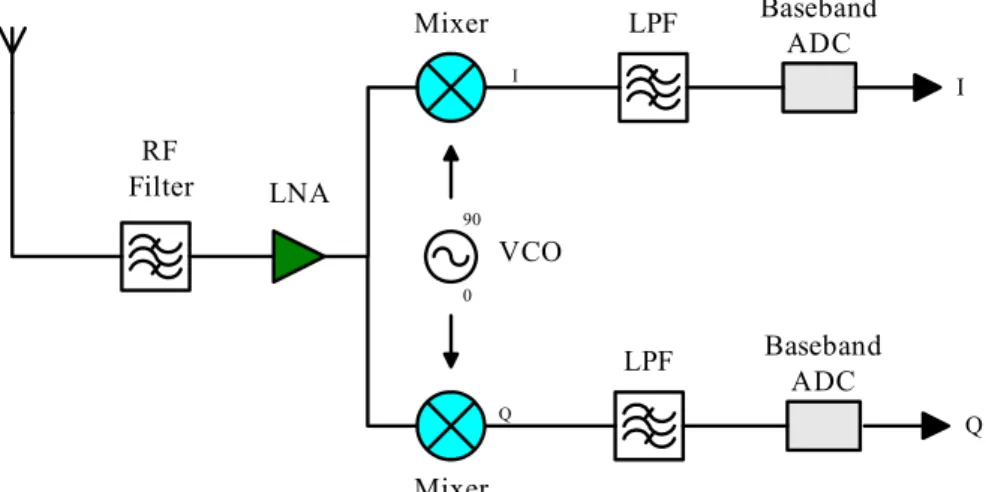
Because of the rapid growth in demand for broadband wireless communications, wireless local area networks (WLAN) are becoming more attractive not only to exchange large amount of data locally but also as access points for the cellular infrastructure. The superheterodyne has been the architecture of choice for wireless transceivers for many years. On the other hand, due to the increase of the integration level of RF front-ends, alternative architectures, targeting reduced power consumption and minimization of the number of off-chip components, have been considered, in the recent past. Among them, the direct conversion receiver (DCR) or zero-IF receiver has increasingly gained widespread attention due to its potentially of low power consumption, lower complexity, low manufacturing costs, and easy integrating with the baseband circuits [4]-[8]. Fig. 2.4 shows the block diagram of the direct conversion RF front-end, where the LO frequency is equal (or approximate) to input carrier frequency and the LO will translate the center of the desired signal to zero IF or low IF.
RF Filter LNA LPF LPF VCO 90 0 Mixer Mixer I Q Baseband ADC Baseband ADC I Q
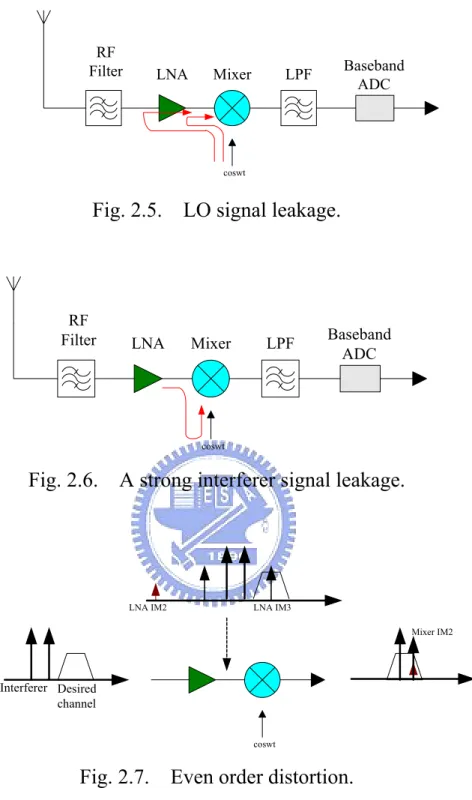
The most important advantage of the direct conversion receiver is that the intermediate frequency (IF) passband filter can be neglected and replaced by a low pass filter. Low pass filter is much easier to integrate in standard semiconductor technology. However, some issues which do not exist or are not serious in the heterodyne architecture become critical in the direct conversion receiver. These drawback include DC offset, flicker noise, even order distortion, I/Q mismatch, and so on. Among these the DC offset generated by self-mixing is the most critical. The DC offset is caused by carrier leakage from the local oscillator to the mixer input and to the antenna as shown in Fig. 2.5. Interferer leakage will also cause a DC offset at the mixer output as shown in Fig. 2.6. To overcome the drawback of DC offset, the improving isolation between LO and RF ports is important. The second-order intermodulation distortion (IMD2) is a fundamental problem, because the second-order intermodulation term interferes the reception of the wanted signal as shown in Fig. 2.7. In a perfectly balanced Gilbert cell mixer, the IMD2 is a common-mode signal and therefore does not a serious problem. However, due to the mismatch of device, the balance between the negative and positive branch of the mixer is degraded and the IMD2 becomes a problem. About I/Q mismatch, if the modulation is complex modulation, the I/Q mismatch can equal to image interferer. This mismatches between the amplitudes of the I and Q signal corrupt the constellation of the down converted signal. Therefore influences the bit error rate. Finally, flicker noise or l/f-noise may be a problem in the mixer and subsequent filter because the signal is converted directly to baseband.
RF
Filter LNA LPF
coswt
Mixer Baseband ADC
Fig. 2.5. LO signal leakage.
RF
Filter LNA LPF
coswt
Mixer Baseband
ADC
Fig. 2.6. A strong interferer signal leakage.
Desired channel
coswt
Interferer
LNA IM2 LNA IM3
Mixer IM2
2.3 The Basic Low Noise Amplifier
2.3.1 The analysis of transistor noise model [9]
The dominant noise source in CMOS devices is channel noise, which basically is thermal noise originated from the voltage-controlled resistor mechanism of a MOSFET. This source of noise can be modeled as a shunt current source in the output circuit of the device. The channel noise of MOSFET is given by
( d2) 4 0 d i kT g f = γ Δ (2.1)
where γ is bias-dependent factor, and gd0 is the zero-bias drain
conductance of the device. Another source of drain noise is flicker noise and is given by equation 2.2.
2 2 2 2 m n T ox g K K i f A f f WLC f ω = ⋅ ⋅ Δ ≈ ⋅ ⋅ ⋅ Δ (2.2)
Hence, the total drain noise source is given by 2 2 0 2 4 m nd d ox g K i kT g f f f WLC γ = Δ + ⋅ ⋅ Δ (2.3) At RF frequencies, the thermal agitation of channel charge leads to a noisy gate current because the fluctuations in the channel charge induce a physical current in the gate terminal due to capacitive coupling. This source of noise can be modeled as a shunt current source between gate and source terminal with a shunt conductance gg, and may be
expressed as
2 4
n g g
i = kT gς Δf (2.4)
where the parameter gg is shown as
2 2 0 5 gs g d C g g ω = (2.5) and δ is the gate noise coefficient. This gate noise is partially correlated with the channel thermal noise because both noise currents stem from thermal fluctuations in the channel, and the magnitude of the correlation
can be expressed as * 2 2 0.395 g d g d i i c j i i ⋅ ≡ ≈ ⋅ (2.6)
where the value of 0.395j is exact for long channel devices. Hence, the gate noise can be re-expressed as
2 2 2
(
2)
( ) 4 4 1
ng ngc ngu g g
i = i +i = kT gς Δf c + kT gς Δf − c (2.7)
where the first term is correlated and the second term is uncorrelated to channel noise. From previous introduction of MOSFET noise source, a standard MOSFET noise model can be presented in Fig. 2.8, where 2
n d
i
is the drain noise source, 2
n g
i is the gate noise source, and Vrg2 is
thermal noise source of gate parasitic resistor rg .
Fig. 2.8. A noise model of MOSFET 2.3.2 The basic of low noise amplifier
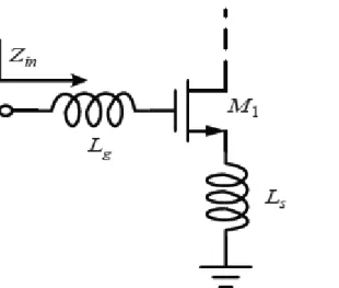
Low noise amplifier is the first gain stage in the receive path so its noise figure directly adds to that of the system. Therefore, there are several common goals in the design of LNA. These include minimizing noise figure of the amplifier, providing enough gain with sufficient linearity and providing a 50 ohm input impedance to terminate an unknown length of transmission line which delivers signal from antenna to the amplifier [10]. Among LNA architectures, inductive source degeneration is the most popular method since it can achieve noise and power matching simultaneously, as shown in Fig. 2.9.
Fig. 2.9 common-source input stage with inductive source degeneration
2.4 Mixer Fundamentals 2.4.1 Principles of Mixer
The mixer is an essential building block in the receivers, which is responsible for frequency up-conversion and down-conversion. It is also an important component associated with the linearity of the front-end receivers. The first stage of mixer must have high linearity to handle the large input signals from LNA without significant intermodulation. Nonlinearity causes many problems, such as cross modulation, desensitization, harmonic generation, and gain compression, but even-order nonlinearity can be easily reduced by differential architecture. However, odd-order nonlinearity is difficult to be reduced, especially the third-order intermodulation distortion (IMD3). IMD3 is the dominant part of the odd-order nonlinearity.
Mixer is a three ports circuit, which are the RF port, the LO port and the IF port. It is a multiplication of two signals which are the RF signal amplified from the low noise amplifier and the signal from the local oscillator (LO) to achieve the function of frequency transformation. This
is depicted by equation (2.8). Then the RF signal is down-converted to the intermediate frequency (IF).
(
cos 1)(
cos 2)
2 cos(
1 2)
cos(
1 2)
AB
A ωt B ωt = ⎡⎣ ω ω+ t+ ω ω− t⎤⎦ (2.8)
From the equation (2.8), the multiplication of two signals at the frequencies of ω1 and ω2 together produce signals at the sum (ω1+ω2) and difference (ω1-ω2) frequencies. The amplitudes are proportional to the RF and LO amplitudes. The multiplications in the time domain would result in convolutions in the frequency domain. Thus, the mixer can responsible for frequency translation. In equation (2.8), signals at the frequency of (ω1+ω2) can be easily filtered out because they are far away from desired frequency in the frequency domain. The signals at the frequency of (ω1-ω2) are our desired outputs. In circuit implementations, the multiplication can be achieved by passing the input signal Acosω t
from RF through a switch driven by another signal Bcosω t from LO. If
the LO amplitude is constant, any amplitude modulation in the RF signal is transferred to the IF signal.
The most important parameters for determining the performance of a mixer are power conversion gain, and linearity. We will describe these parameters in the subsequent contents.
2.4.2 Performance Parameters 2.4.2.1 Conversion Gain
One of important parameters of mixer’s characteristics is conversion gain, which is defined as the ratio of the desired IF output to the value of the RF input as shown in equation (2.9). In general, the conversion gain
of the mixer has two types: one is voltage conversion gain and the other is power conversion gain.
The desired output IF power Conversion Gain
The input RF power
= (2.9)
Assuming input a sinusoidal signal and the output would include signals at integer multiples of the frequencies of the input signal as equation (2.10). In equation (2.10), the terms with the input frequency are called the fundamental signal, and the higher order terms are called the harmonics. The harmonics would cause performance degradations.
( ) ( ) ( ) ( ) ( ) ( ) 2 3 1 2 3 3 2 3 2 1
( ) cos cos cos ...
cos 1 cos 2 3cos cos3 ...
2 4 OUT V t A t A t A t A A A t t t t α ω α ω α ω α α α ω ω ω ω = + + + = + + + + + (2.10)
The output function of mixers is a compressive function of input levels. When the input level grows sufficiently high, the output eventually saturates and the conversion gain begins decreasing. If α3 holds a negative value, this phenomenon will happen. At small values of input level A, the second term is negligible and the gain remains constant. The gain starts decreasing when the input level gets large as shown in equation (2.11). 2 3 1 4 A Gain=α +α (2.11) 2.4.2.2 Linearity
The mixers are assumed to be linear and time-invariant. The linearity is a significant parameter in the mixer design. Here we will introduce two parameters of linearity: P1dB and IIP3.
ideally. However, as the input signal becomes large, the output signal fails to exhibit this characteristic. We use the value departing the ideal linear curve 1 dB as the referenced point, 1 dB compression point, shown in Fig. 2.10. The dashed line in Fig. 2.10 shows our desired output characteristics. The solid line shows the real characteristic. The 1dB compression point characterizes the input level where the output level is 1dB less than our desired output level. A higher 1dB compression point stands for a better linearity performance.
The linearity of a mixer can also be evaluated by intermodulations. The two-tone third-order intercept is often used to characterize mixer linearity. Ideally, each of two different RF input signals will be translated without interacting with each other, and we can only gain the desired IF signal from the output port. However, practical mixers will always exhibit some intermodulation effects. This is because that two or more different frequencies of input signals will degrade the linear region of the system. The third intercept point (IP3) is measured with two tone test. Two tones are closely placed and injected as input simultaneously. If we consider the region where the input level is small, the output characteristic is approximately linear. The third-order intercept is the intersection of these two curves as illustrated in Fig. 2.11 which is the extrapolation of the signal line and the third-order harmonic line. The higher intercept, the more linear.
1dB A 1dB RF input power IF output power Fig. 2.10 P1dB. 3rd intercept point RF input power IF output power 3rd intermodulation product IF power Fig. 2.11 IIP3. 2.4.2.3 Isolation
Another important parameter of mixer is isolation, which shows the interaction among RF, IF and LO ports. The isolation between each two ports of the mixer is important. The LO to RF feedthrough is means the LO leakage to the LNA and (or) leakage to the antenna. The RF to LO feedthrough allows strong interferers in the RF path to interact with the LO driving the mixer. The LO to IF feedthrough is also important. If substantial LO signal exists at the IF output, the following stage may be desensitized. The feedthrough can be reduced largely by use double balanced mixers. The RF to IF isolation means the signal in the RF path
directly appears in the IF. In the homodyne receivers, this is a critical issue with respect to the IMD2 problem.
2.4.3 Mixer Architecture
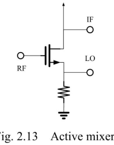
The implementation of CMOS down-conversion mixer can be passive or active. The simple passive mixer is shown in Fig. 2.12. It is usually using MOS transistor as a switch to modulate the RF signal by LO signal and down convert to IF band. Because passive mixer operates in the linear region, it has high linearity and excellent IIP3. But it provides poor conversion gain and noise figure. The simple active mixer is presented in Fig. 2.13. The active mixer provides better conversion gain than passive mixer. Its conversion gain is decided by the product of the input conductance gm and load impedance to suppress the noise
contributed by the subsequent stages. But the linearity of an active mixer is worse than that of a passive mixer.
RF
LO
IF
IF
RF
LO
Fig. 2.13 Active mixer.
The Gilbert cell topology is a typical type used in active mixers. The advantages of this topology are the high conversion gain, low LO power, and low offset voltage. The Gilbert cell mixer consists of three stages: transconductor stage, switching stage, and load stage. The linearity of Gilbert mixer is dominated by the transconductor stage as shown in Fig. 2.14. RF + RF -LO + LO + LO -Load stage Switching stage Transconductor stage
Fig. 2.14 The prototype of the CMOS Gilbert mixer
The function of three stages is described as follow. RF input stage is a differential pair that converts the RF voltage to current. The transconductance of this stage directly affects the linearity and the gain of
the mixer. LO switch stage usually applies two differential pairs as modulated switch to construct double balanced structure. To achieve the goal that this two differential pairs completely switch the input power of the LO port must be larger. The value of the LO port also affects the conversion and the noise figure of the system. The output stage is load stage.
If the switching stage is ideal switches, the linearity of Gilbert mixer is dominated by the transconductor stage. Third-order input intercept point (IIP3), second-order input intercept point (IIP2), and input 1-dB compression point (P1dB) are the important parameters of linearity. IIP3 and IIP2 are the effects of intermodulation terms in the nonlinear circuits. P1dB is the ceiling of the input power. To improve linearity in Gilbert mixer, many methods have being used such as adding source degeneration resistors below the gain stage [11], bisymmetric Class-AB input stage [12], multiple gated transistor [13], and common-source and common-emitter RF transconductors [14].
2.5 The Review of VCO 2.5.1 Principles of VCO
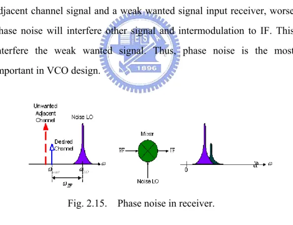
Voltage controlled oscillator is essential building block in communication systems. The VCO is used as local oscillator to up-conversion or down-conversion signals. The phase noise is the main
the most important.
Oscillator can transfer DC power to AC power. Oscillator is an energy transfer device. For steady oscillation, the self-oscillating system must be satisfied Barkhausen’s criteria: ( )H jω0 =1 and ( )
0 0 0
H jω
∠ = (or
1800 of dc feedback is negative). There are two types of analysis methods: positive feedback and negative resistance. In the design of oscillator, the important performance parameters are phase noise, output power, tuning range, and thermal stability. Among these parameters, the most important is the phase noise. Phase noise will influence the signal quality in receiver as shown in Fig. 2.15. When a strong unwanted adjacent channel signal and a weak wanted signal input receiver, worse phase noise will interfere other signal and intermodulation to IF. This interfere the weak wanted signal. Thus, phase noise is the most important in VCO design.
Fig. 2.15. Phase noise in receiver.
LC tank voltage-controlled oscillator and ring oscillator are the two most popular circuits in VCO design. LC tank voltage-controlled oscillator has better phase noise, but tuning range is narrow. Ring oscillator has wider tuning range, but phase noise is worse. We will
introduce these two types as following section.
2.5.1.1 LC Tank Voltage-Controlled Oscillator
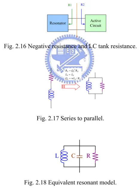
The concept of LC tank VCO is using negative resistance of active circuit to cancel the resistance of LC tank as shown in Fig. 2.16. Fig. 2.17 shows series transfer to parallel. Fig. 2.18 shows its equivalent resonant model. LC tank oscillator is called negative-Gm oscillator.
Resonator CircuitActive R1 R2
Fig. 2.16 Negative resistance and LC tank resistance.
Fig. 2.17 Series to parallel.
L C R
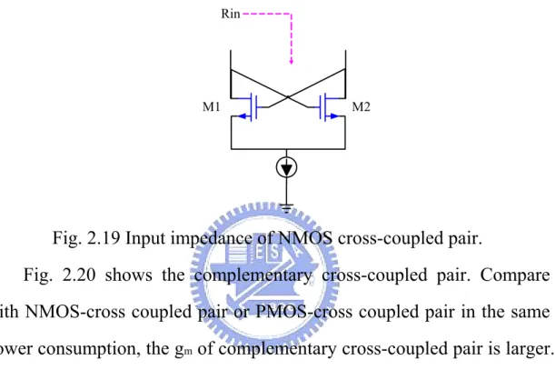
is positive feedback. In Fig. 2.19, we can calculate the impedance seen at the drain of M1 and M2. The impedance is
m
in g
R =−2 . Generally speaking,
the phase noise of PMOS-cross coupled pair is better than NMOS-cross coupled pair.
M1 M2
Rin
Fig. 2.19 Input impedance of NMOS cross-coupled pair.
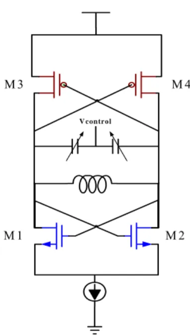
Fig. 2.20 shows the complementary cross-coupled pair. Compare with NMOS-cross coupled pair or PMOS-cross coupled pair in the same power consumption, the gm of complementary cross-coupled pair is larger.
Larger gm means faster switching. The rise-time and fall-time of output waveform are more symmetric and the phase noise is better.
M 1 M 2 V con trol
M 3 M 4
Fig. 2.20 Complementary cross-coupled pair.
2.5.1.2 Ring Oscillator
Fig. 2.21 shows the ring oscillator. It is cascade of N stages with an odd number of inverters is placed in a feedback loop. The period of ring oscillator is equal to 2NTd and the oscillation frequency is
d NT f 2 1 0 = .
There are three advantages of the ring oscillator: high integrated with PLL, smaller die size than LC-tank VCO, and full output voltage swing.
Fig. 2.21 Ring oscillator.
2.5.2.1 Phase Noise
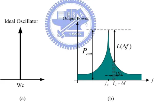
An ideal output spectrum of oscillator has only one impulse at the fundamental frequency as shown in Fig. 2.22(a). In an actual oscillator, the frequency spectrum consists of an impulse exhibits skirts around the carrier frequency as show in Fig. 2.22(b). These skirts are called phase noise due to the influence of several kinds of noises. The noise sources such as shot noise, flicker noise and thermal noise. These noises are caused by the resistors, capacitors, inductors, and transistors. Noise injected into an oscillator by noise sources may influence the frequency and the amplitude of the output signal. These phenomenon are called AM, PM and FM noises. Ideal Oscillator Wc f Output Power f fC+Δ C f Hz 1 ) ( f L Δ out
P
(a) (b)Fig. 2.22 Output spectrum of ideal and actual oscillators.
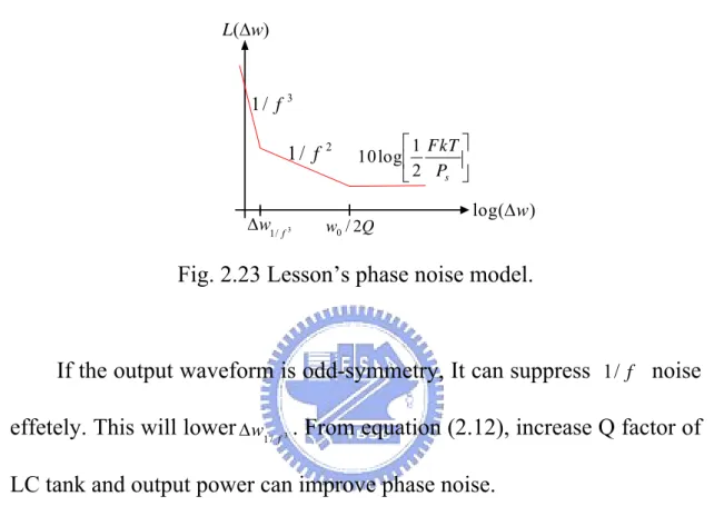
Fig. 2.23 shows the Lesson’s phase noise model. We can express by
3 2 1/ 1 ( ) 10log 1 1 2 2 f o s FkT L P Q ω ω ω ω ω ⎡ ⎧⎪ ⎡ ⎤ ⎫⎪⎤⎡ Δ ⎤ ⎢ ⎥ Δ = ⎨ +⎢ ⎥ ⎬ ⎢ + ⎥ Δ Δ ⎢ ⎪⎩ ⎣ ⎦ ⎪ ⎣⎭⎥ ⎢ ⎥⎦ ⎣ ⎦ (2.12)
This equation is from the curve fitting after measured results of VCO. Therefore, Δω1/ f3 is from measured results.
) log( wΔ ) ( w L Δ 3 / 1 f 2 / 1 f ⎥ ⎦ ⎤ ⎢ ⎣ ⎡ s P FkT 2 1 log 10 3 / 1 f w Δ w0/2Q
Fig. 2.23 Lesson’s phase noise model.
If the output waveform is odd-symmetry, It can suppress 1/ f noise
effetely. This will lowerΔw1 f/ 3. From equation (2.12), increase Q factor of
LC tank and output power can improve phase noise.
2.5.2.2 Frequency Tuning Range
Frequency variation is an important parameter when designing VCO. Because a CMOS oscillator must be designed with a large tuning ranges to overcome process variations. The simplest way to do so is with a varator such as diode varator and MOS varator. The NMOS cross-coupled pair VCO has higher tuning range than double cross-coupled VCO topology for equal effective tank transconductance.
When control voltage change, the bias voltage of transistor will also change. S parameter and Γ will change according to dc current
variation. This will cause output frequency shift. This is called pushing effect. To avoid pushing effect, we can use high quality resonator to reduce the pushing effect. We can also using regulator to overcome pushing effect such as band gap circuits.
Loading effect is another problem. When loading change, its impedance is also change. This will cause output frequency shift. This is called load pulling effect. To avoid this problem, we can use buffer circuit to overcome load pulling effect.
2.5.3 Noise Model of VCO
Phase noise is the most important parameter in the VCO design. There are two models: Leeson’s model and Hajimiri model. Lesson has developed a time invariant model to describe the noise of oscillators. Hajimiri proposed a linear time varying phase noise model. The below sections will introduce these two phase noise model.
2.5.3.1 Time Invariant Model
In this section, phase noise analysis is described by using time invariant model. Time invariant means whenever noise sources injection, the phase noise in VCO is the same. In other words, phase shift of VCO caused by noise is the same in any time. Therefore, it’s no need to consider when the noise is coming. Suppose oscillator is consists of amplifier and resonator. The transfer function of a bandpass resonator is written as 2 (1/ ) ( ) (1/ ) (1/ ) j RC H j LC j RC ω ω ω ω = + − (2.13)
2 2 ( / ) ( ) ( / ) o o o j Q H j j Q ω ω ω ω ω ω ω = + −
(2.14)
Compare equation (2.13) with (2.14). Thus,
1/ Q=
o LC oRC
ω = and ω
(2.15)
The frequency ω ω= o + Δω which is near oscillator output
frequency. Ifωo Δω , we can use Taylor expansion for only first and
second terms. Hence
2 ( ) 1 ( o/ ) H j j Q ω ω ω ≈ + ⋅ Δ
(2.16)
The close-loop response of oscillator is expressed by
( / ) 1 ( ) 1 ( ) 2 o j Q G j H j ω ω ω ω − = ≈ − ⋅ Δ
(2.17)
When input noise density is Si( )ω , the output noise density is
2 2 ( ) ( ) ( ) ( ) 2 o o i S S G FkT Q ω ω ω ω ω = = Δ
(2.18)
The above equation is double sideband noise. The phase noise faraway center frequency Δω can be expressed by
2 2 ( ) 10 log 2 o s FKT L P Q ω ω ω ⎡ ⎛ ⎞ ⎤ Δ = ⎢ ⋅⎜ ⎟ ⎥ Δ ⎢ ⎝ ⎠ ⎥ ⎣ ⎦
(2.19)
where Ps is the output power. From equation (2.19), increasing
power and higher Q factor can get better phase noise. Increasing power means increasing the power of amplifier. This will decrease noise figure (F) and improve phase noise.
From equation (2.19), we can briefly understand phase noise. But the equation and actual measured result are different. The VCO spectrum is shown as Fig. 2.23. The phase noise equation can be modified as
3 2 1/ 2 ( ) 10log 1 1 2 f o s FKT L P Q ω ω ω ω ω ⎡ ⎧⎪ ⎛ ⎞ ⎫⎛⎪ ⎞⎤ ⎢ ⎥ Δ = ⎢ ⋅ +⎨ ⎜ Δ ⎟ ⎜⎬⎜ + Δ ⎟⎟⎥ ⎝ ⎠ ⎪ ⎪⎝ ⎠ ⎩ ⎭ ⎣ ⎦
(2.20)
The above equation is called Leeson’s model.
2.5.3.2 Time Variant Model
In this section, we use the Hajimiri model to explain the phase noise. At first, we assume that an impulse current injects into a lossless LC tank as illustrated in Fig. 2.24. If the impulse happens to coincide with a voltage maximum as shown in top of Fig. 2.25. The amplitude increase ΔV=ΔQ/C, but the timing of the zero crossings does not change. An impulse injected at any other time displaces the zero crossings as shown in bottom of Fig. 2.25. Hence, an impulsive input produces a step in phase, so that integration is an inherent property of the impulse to phase transfer function. Because the phase displacement depends on when the impulse is applied, the system is time-varying.
L C i(t) ) ( τ δt− i(t) t
t V o u t V Δ τ t V o u t V Δ τ ( a ) ( b )
Fig. 2.25 Waveforms for impulse excitation.
Hajimiri proposed a linear time-varying phase noise model which is different from the Lesson’s model. The impulse response can be written as max ( ) ( , ) o ( ) h t u t q ω τ φ τ =Γ −τ
(2.21)
where qmax is the maximum charge displacement across the
capacitor and u(t) is the unit step. The function Γ( )x is called the
impulse sensitivity function (ISF), and is a frequency and amplitude independent function that is periodic in 2π. Once the ISF has been determined, we may compute the excess phase through use of the superposition integral. Hence
max 1 ( ) ( , ) ( ) ( ) ( ) t o t h t i d i d q φ φ ∞ τ τ τ ω τ τ τ −∞ −∞ =
∫
=∫
Γ(2.22)
This equation can be expanded as a Fourier series: 0 1 ( ) cos( ) 2 o n o n n c c n ω τ ∞ ω τ θ = Γ = +
∑
+(2.23)
harmonic of the ISF. We assume that noise components are uncorrelated, so that their relative phase is irrelevant, we will still ignoreθn. Equation
(2.23) can be rewritten as 0 1 max 1 ( ) ( ) ( )cos( ) 2 t t n o n c t i d c i n d q φ τ τ ∞ τ ω τ τ = −∞ −∞ ⎡ ⎤ = ⎢ + ⎥ ⎣
∫
∑
∫
⎦(2.24)
Equation (2.24) allows us to compute the excess phase caused by an arbitrary noise current injected into the system, once the Fourier coefficients of the ISF have been determined. Now we consider the injection of a sinusoidal current whose frequency is near an integer multiple m of the oscillation frequency, so that
[
]
( ) mcos ( o )
i t =I mω + Δω t
(2.25)
Substituting (2.25) into (2.24) where Δ ω ωo and n=m. We can
simplify Equation (2.24) as max sin( ) ( ) 2 m m I c t t q ω φ ω Δ ≈ Δ
(2.26)
[
]
( ) cos ( ) out o V t = ωt+φ t(2.27)
Substituting (2.19) into (2.20). Suppose max 1 2 m m I c q Δω < . Therefore, the
sideband power relative to the carrier is given by
2 max ( ) 10 log 4 m m SBC I c P q ω ω ⎛ ⎞ Δ ≈ ⎜ ⎟ Δ ⎝ ⎠
(2.28)
In general, a noise signal can be separated into two type noise source: white noise and flicker noise. First, input an noise current only with the white noise and its noise power spectral density is
2
n
i f
Δ . The total single sideband phase noise spectral density in dB below the carrier per unit
bandwidth is given by 2 2 0 2 2 max ( ) 10 log 4 n m m SSB i c f C q ω ω ∞ = ⎛ ⎞ ⎜ ⎟ Δ ⎜ ⎟ Δ ≈ ⎜ ⎟ Δ ⎜ ⎟ ⎜ ⎟ ⎝ ⎠
∑
(2.29)
According to Parseval’s theorem. Thus, 2 2 2 2 0 0 1 ( ) 2 m rms m c x dx π π ∞ = = Γ = Γ
∑
∫
(2.30)
Therefore we can use quantitative analysis to analyze the phase noise sideband power due to the white noise source as following equation
2 2 2 2 max ( ) 10 log 2 n rms i f L q ω ω ⎛ ⎞ Γ ⎜ ⎟ Δ ⎜ ⎟ Δ ≈ ⎜ ⎟ Δ ⎜ ⎟ ⎜ ⎟ ⎝ ⎠
(2.31)
where qmax=CVmax , Vmax is the largest amplitude of VCO, and
2 4
n
i kT
f = R
Δ . Substituting these relations into (2.31). We have
2 2 4 ( ) 10log o rms s kT L P Q ω ω ω ⎛ ⎛ ⎞ ⎞ ⎜ ⎟ Δ ≈ Γ ⎜ ⎟ ⎜ ⎝ Δ ⎠ ⎟ ⎝ ⎠
(2.32)
If input noise of VCO is 1/f noise, the power spectral density is written as 1/ 2 2 ,1/ f n f n i i ω ω = Δ
(2.33)
whereω1/ f is the 1/f corner frequency of 1/f noise. This equation represents the phase noise spectrum of an arbitrary oscillator in 1/f2 region of the phase noise spectrum. Quantitative analysis for the relationship between the device corner 1/f and the 1/f 3 corner of the
2 2 0 1/ 2 2 max ( ) 10log 8 n f i c f L q ω ω ω ω ⎛ ⎞ ⎜ ⎟ Δ ⎜ ⎟ Δ ≈ ⎜ ⋅ ⎟ Δ Δ ⎜ ⎟ ⎜ ⎟ ⎝ ⎠
(2.34)
Fig. 2.26 Conversion of noise to phase noise sidebands.
Here we consider the case of a random noise current in(t) whose power
spectral density has both a flat region and a 1/f region as shown in Fig. 2.26. Noise components located near integer multiples of the oscillation frequency are transformed to low frequency noise sidebands for SΦ(ω)
and it’s become phase noise in the spectrum of SV(ω) as illustrated in Fig.
2.26. It can be seen that the total SΦ(ω) is given by the sum of phase noise
contributions from device noise of the integer multiples of ωo and
weighted by the coefficients cn. The theory predicts the existence of 1/f 2,
noise sources are weighted by the coefficient c0 and show a dependence
on the offset frequency. The white noise terms are weighted by other cn
coefficients and give rise to the 1/f 2 region of phase noise spectrum. From Fig. 2.26, it is obviously that if the original noise current i(t) contains 1/fn low frequency noise terms, they can appear in the phase noise spectrum as 1/fn+2 regions.
Mp
Mn
RF_in RF_out
Chapter 3 The Design of LNA with Notch Filters for UWB
Wideband systems are quite sensitive to out-of-band blockers. In particular, UWB systems require mitigation of the interference caused by WiFi systems operating in the 2.5GHz and 5.2GHz bands because the power of WiFi systems can exceed received UWB signal power a lot. As such, filtering of the interferers is beneficial to relax the linearity requirements of the downconversion mixer, and to avoid receiver gain desensitization.
3.1 Circuit Design of the UWB LNA with low power 3.1.1 Input-matching stage
In input stage, we first use the current-reused structure by cascading PMOS and NMOS which is shown in Fig. 3.1 to achieve the twice power gain without extra current consumption [15].
Fig. 3.1 Schematic of the cascade structure
Mp Mn RF_in RF_out Rf Mp Mn RF_in RF_out Rf Ls Ls
shunt feedback resistance Rf in the input stage shown in Fig. 3.2(a).
Since, the S11 in Fig. 3.2(b) move to the center of smith chart.
Fig. 3.2(a) Schematic with Rf (b) S(1,1) with Rf and without Rf
For reaching input-matching further, as shown in Fig. 3.3(a), the inductance Ls is added to the source of input stage and the improvement
of S11 is shown in Fig. 3.3(b). After adding Rf and Ls, we can accomplish
the whole wideband input-matching network.
Mn Mn Cd Cg Cd Cg R R LH Mn Cg Cd R LS LH 3.1.2 Output-matching stage
Fig. 3.4 Time-domain step current responses in (a) simple RC and (b) shunt peaking inter-stage networks.
When the beginning of the small signal current flowing out from M1 shown in Fig .3.4(a). It will see the impedance of the load resistance
RL and the parasitic capacitances of M1 and M2 and charge them.
Oblivious, we can reduce the current at the start flowing through the load resistance by adding the series inductance LH which is shown in Fig.
3.4(b) . Since, the current will charge the parasitic capacitance quickly to shorten the rising time. As a result, the bandwidth can be extended successfully [16].
networks.
Furthermore, when putting another inductor Ls between the two
parasitic capacitances shown in Fig. 3.5, the current at the start will only charge the Cd so that the bandwidth will be extended more. The
schematic is shown in Fig. 3.6.
Fig. 3.6 the schematic of input-matching and output matching
3.1.3 Noise analysis
Because the noise from substrate of transistor always attributes the noise figure of LNA, we add a large resistance Rb between source and
body of each transistor to improve the noise figure which is shown in Fig. 3.7(a). We can find that it’s very useful for reducing the noise figure in Fig. 3.7(b).
2 4 6 8 10 0 12 -30 -25 -20 -15 -10 -5 -35 0 freq, GHz d B (S (1 ,1 )) with R increasing 2 4 6 8 10 0 12 10 15 20 5 25 freq, GHz dB (S (2 ,1 )) with R increasing 2 4 6 8 10 0 12 5 10 15 0 20 freq, GHz Noi se_ F igu re with R increasing
Fig. 3.7 (a) Schematic with Rb (b) Improvement of the noise figure
It is also important to note that the feedback resistance Rf have
outstanding effect for the noise figure of the LNA. In Fig. 3.8, we can find that the larger value of Rf, the lower noise figure and better power
gain can be reached. But it makes the S(1,1) worse at the same time which is shown in Fig. 3.9. The trade off between the noise figure and the S(1,1) is the main consideration to determine the feedback resistance Rf..
Fig. 3.8(a)Noise figure with different Rf (b)S(2,1) with different Rf
3.2 The Integration of LNA with Notch Filters
3.2.1 The design of notch filters with active inductors
Because WiFi system is a narrow band application, we can only use narrow band filters to suppress WiFi signals to avoid effecting UWB system.
In Fig.3.9, we can find that the Q factor of series resonant is proportional to inductance value and has an inverse ratio with parasitic resistance [17]. In general, the larger inductance value can increase Q factor of series resonant. However, instead of improving Q factor, the performance of filter becomes worse because of the increase of parasitic resistance which is shown in Fig.3.10
0 0
0
sec
L
average energy stored
Q
energy loss per
ond
R
ω
ω
ω
ω
≡
=
=
Δ
0 1 2 3 4 5 -16 -12 -8 -4 0 S 21 (d B ) Frequency (GHz) L=4nH L=2nH L=1nH
Fig.3.10 The filtering ability with increase inductance value
In Fig.3.10, we can find the filtering ability is manly determined by the Q factor so that we add the negative resistance
m
g
2
− to eliminate the
positive resistance of the inductance which is shown in Fig.3.11. Because the negative resistance
m
g
2
− may far bigger than positive
resistance, we use parallel structure shown in Fig.3.11(c) to avoid the system becoming unstable. The design of suppressing circuit is shown in Fig.3.12.
C
1L
1C
1L
1 m g 2 − R −C
1L
1 m g 2 −(a)
(b)
(c)
L
1 2 2 1 2 4 1 2 m m g C w g + −≈
1 2 2 1 4 Cw g C+ mM5 M4 VG1 VDD L1 C1 m g 2 −
Zin
Zin
L1 C1Fig.3.12 The design of suppressing circuit
Using negative resistance can improve the Q factor, but it need more current consumption. To save chip area and power consumption, we realize the inductance by active circuit which is shown in Fig.3.13. It’s consists of two transconductor amplifiers and a capacitor. We can use Kirchhoff equation to derive equivalent inductance value described in equation (1), (2) and (3). A general active inductor is shown in Fig.3.14.
2 1
1
...(1)
X m m XI
G
G V
sC
⎛
⎞
−
= −
⎜
×
⎟
⎝
⎠
1 2/(
) ...(3)
eq P m mL
=
C
G
⋅
G
1 2...(2)
X X m mV
sC
sL
I
=
G G
=
Fig.3.13 The concept of active inductor
2 1 1 2 1 2 1 1 2 ; ds m gs gs m m ds s m m G g g C C C L g g g R g g ≈ + = = =
Fig.3.14 The schematic of the active inductor
In Fig.3.15, we use resistance Rf to improve the Q factor by
reducing the loss of the inductor and increasing the inductance value. Additionally, using a plus transistor M3 to raise feedforward character can
make the Q factor better shown in Fig.16. The final improved schematic is shown in Fig.17.
1 2 1 1 2 1 1 2 1 1 2 1 (1 ) m ds ds f gs gs ds f m m ds s m m g G g g R C C C g R L g g g R g g ≈ + + = + ≈ ≈
Fig.3.15 Active inductor with additional Rf
The basic theory to suppress WiFi signal is use series LC tank shorting only when the frequency is
LC
π
2
1 . It is nearly regarded as
open circuit when the frequency is far away from
LC
π
2
1 . We can use
this character to filter the frequencies of 2.5GHz and 5.2GHz in different paths shown in Fig.3.18. We can find the simulation results by using ideal inductances and capacitors in Fig.3.19.
Fig.3.18 The basic concept of suppressing WiFi signals
3.2.2 The total design with small area and low power
When mixing the LNA and filters, the total noise figure would become very high if the filters are added in front of the LNA. So we finally determined adding the filters after the LNA which is shown in Fig.3.20. In additional, we avoid using any passive inductances and only using the feedback resistance RFB to achieve input-matching to save chip
area. The core area of this design is only 0.0016mm2.
3.3.1 Simulation and Measured Results of LNA
Fig.3.21 shows the magnitude of S11 and S21. Fig.3.22 shows the
magnitude of P1dB. The characteristic of the proposed LNA was verified from Fig.3.21 and Fig.3.22. Fig.3.23 shows the noise figure of the design. Table 3.1 summarizes the performance of measured results.
Fig.3.21 The magnitude of S11 and S21
Fig.3.22 The magnitude of P1dB
x
Table 3.1 Measurement results of LNA
specification This work
Technology 0.18-um CMOS
Frequency(GHz) 3.1-10.6
Input return loss S11(dB) <-6.4
Supply voltage(V) 1.4 Power gain(dB) 9.5-14.5 Reverse isolation S12(dB) <-40 NFmin(dB) 2.6 Bandwidth(GHz) 1.6-10 P1dB@7GHz -14 Pdiss(mW) *6.8 Chip Area 0.66mm2 *exclude buffer
3.3.2 Simulation and Measured Results of LNA with notch filters Fig.3.24 shows the magnitude of S11 and S21. Fig.3.25 shows the
noise figure of the design. The characteristic of the proposed LNA with notch filters was verified from Fig.3.24 and Fig.3.25. Table 3.2 summarizes the performance of simulation and measured results.
Fig.3.24 The magnitude of S11 and S21 for LNA with notch filters
Table 3.2 Comparison of LNA
specification This work
Technology 0.18-um CMOS
Frequency(GHz) 3-5
Input return loss S11(dB) <-7.5
Supply voltage(V) 1.8 Power gain(dB) 10.1-13.9 Notch performance @2.5GHz、5.2GHz 19dB/ 38dB Reverse isolation S12(dB) <-40 NFmin(dB) 2 Bandwidth(GHz) 3-5 P1dB -14.2 Pdiss(mW) 10.3
Chip Core Area 0.0016mm2
3.4 Comparison and Summary
The comparison of the proposed low noise amplifier and LNA with notch filters against recently reported on LNA are shown in Table 3.3 and Table 3.4.
Table 3.3 Simulation and measurement results of LNA with filters
specification This work 2007[18]
EL 2007[19] MWCL 2007[20] EuMA Technology 0.18-um CMOS 0.18-um CMOS 0.18-um CMOS 0.18-um CMOS Frequency(GHz) 3.1-10.6 3.1-10.6 3.1-10.6 3.1-10.6 S11(dB) <-5.4 <-9.7 <-8 <-10 Supply voltage(V) 1.4 1.9 1.8 1.4 Power gain(dB) 9.5-14.5 11~11.8 13.5~16 10.5~12.5 Reverse isolation S12(dB) <-40 <-40 <-40 -- NFmin(dB) 2.6 4.12 3.1 4.45 Bandwidth(GHz) 1.6-10 1.3-12.1 3.4-11.4 2-9 P1dB@7GHz -14 -7.86 -- -- Pdiss(mW) *6.8 22.7 11.9 28 Chip Area 0.66mm2 **0.447 mm2 1.2mm2 0.63mm2 *exclude buffer **exclude test pad
Table 3.4 Comparison of LNA with filters
specification This work 2007[21]
ISSCC 2007[22] RFIC 2007[23] EL Technology 0.18-um CMOS 0.13-um CMOS 0.18-um CMOS 0.18-um CMOS Frequency(GHz) 3-5 3-5 3-10 3-10
Input return loss S11(dB) <-7.5 <-10 <-10 <-10 Supply voltage(V) 1.8 1.5 1.8 1.8 Power gain(dB) 10.1-13.9 <19.4 <21.5 <20.3 Notch performance @2.5GHz、5.2GHz 19dB 38dB 6dB 44dB -- <10dB 12.8dB 19.6dB Reverse isolation S12(dB) <-40 -- -- -- NFmin(dB) 2 3.5 3.5 4 Bandwidth(GHz) 3-5 3-5 3-10 2.9-12.3 P1dB -14.2 -9.4 -- -- Pdiss(mW) 10.3 31.5 21.8 24
Chip Core Area *0.0016mm2 1.6mm2 1.2mm2 1.43mm2
Chapter 4 The Integration of Mixer and VCO with Balun
The demand for high speed wireless systems is driven by the growing popularity of consumer products. Low-voltage, low-power, and highly integrated circuits are always the trends for IC design, especially crucial in mobile wireless communication systems due to the limitation of battery capacity. The contents of this chapter below will introduce the integration of mixer, VCO, and Balun using 0.18 um CMOS process in detail and discuss the principles and aonsiderations of each section.
4.1 Circuit Design of the Mixer and VCO with Balun
4.1.1 Analysis of the mixer with current-bleeding method
In general, an active mixer has three stages that involve transconductance stage, switch stage and load stage which is shown in Fig.4.1. We know that increasing the bias current of the transconductance stage makes higher gain and better linearity possible. However, a larger switching current causes voltage headroom issue and larger noise. Therefore, the current bleeding technique is implemented by using two PMOSFETs to reduce the bias current of the switch stage which is shown in Fig.4.1.
Fig. 4.1 Gilbert-type mixer with current bleeding circuits
From (1), if the bias current of switch stage is decreased, the output flicker-noise current generated by the direct mechanism can be minimized. Fig.4.1 shows a double-balanced Gilbert-type mixer with current bleeding circuits. The mixer comprises a transconductance stage, switch stage, load stage and pMOS current bleeding circuit.
, ( ) ( 4 ) ( ) o n d i r I V n i S T × = × (1)
4.1.2 The replacement of current source with VCO
Although the current bleeding technique can minimize the output flicker-noise current and maintain the transconductance gain at the same time, the bleeding current is used up without other profits. The core
idea of this design is to make the bleeding current for VCO use. In other words, we will replace current bleeding circuits with VCO to make current reused which is shown in Fig.4.2. In additional, we change the RF port and LO port for optimal design.
Fig. 4.2 Replace current bleeding circuits with VCO 4.1.3 The addition of the balun
Most balun structures utilize either distributed or lumped elements. Distributed baluns are composed of sections of
λ
/ 2 transmission line or/ 4
λ
coupled line. Theses structure occupy large size especially in the integrated circuit implementation. As lumped element balun is formed with low pass filter, 900 ahead, and high pass filter, 900 behind, it always exhibit poor balun balance across frequency [24].Recently, balun structures consisted of both distributed and lumped elements have been proposed [25]. The balun as shown in Fig. 4.3 has
coupled lines length can been reduced and two poles induce because of the coupled resonators. C1 is the input matching. Fig. 4.4 shows the S-parameter. The phase difference is as shown in Fig. 4.5. Fig. 4.6 shows the die size of proposed balun is about 0.26*0.26mm2.
C1
C2
C3
Fig. 4.3 The schematic of the proposed balun
m3 freq= m3=-8.0385.790GHz 3 4 5 6 7 8 9 2 10 -40 -30 -20 -10 -50 0 freq, GHz d B (S (1 ,1 )) d B (S (2 ,1 )) m3 d B (S (3 ,1) )
m2 freq= m2=-179.3295.870GHz 3 4 5 6 7 8 9 2 10 -100 0 100 200 -200 300 freq, GHz ph a m2
Fig. 4.5 The simulation phase difference of proposed balun
Fig. 4.6 The layout of proposed balun
4.1.4 Total design circuit
Finally, the integration of mixer, VCO, and balun is achieved for optimal current-reused. As shown in Fig. 4.7, we can see the whole
Fig. 4.7 Final proposed schematic of the integration 4.2 Simulation Results
Fig. 4.8 shows the magnitude of S11 and S21. Fig. 4.9 shows the tuning range and phase noise of VCO . The conversion gain and P1dB of the proposed design in 5.2GHz and 5.8GHz are presented from Fig. 4.10 and Fig. 4.11. Table 4.1 summarizes the performance of simulation results.
Fig. 4.8 the magnitude of S11 and S21
(a) Tuning range of VCO
(b) Phase noise of VCO
Conversion gain of 5.2GHz is 15.6dB
(a) conversion gain in 5.2GHz
P1dB of 5.2GHz is -17dB
(b) conversion gain in 5.2GHz Fig. 4.10 conversion gain and P1dB in 5.2GHz
Conversion gain of 5.8GHz is 14.6dB
(a) conversion gain in 5.8GHz
P1dB of 5.8GHz is -16dB
(b) conversion gain in 5.8GHz Fig. 4.11conversion gain and P1dB in 5.8GHz
Table 4.1 Simulation results of mixer and VCO Performance of mixer and VCO with balun
5.2 GHz 5.8 GHz
VDD 1.4 V
Power consumption 6.12 mW
Input return loss 12 dB 16 dB
Output return loss 12 dB 12 dB
Conversion Gain 15.6 dB 16.6 dB
P1dB -17 dB -16 dB
Phase noise -105 dBc/1MHz -105 dBc/1MHz
LO power -8 dBm -6 dBm
4.3 Comparison and Summary
The comparison of the proposed design that contains mixer and VCO with balun against recently reported is shown in Table 4.2.
Table 4.2 Comparison of Mixer and VCO
specification This work 2005[27]
ISCAS 2006[28] MTT 2006[29] EuMA Technology 0.18-um CMOS 0.18-um CMOS 0.18-um CMOS 0.18-um CMOS Frequency(GHz) 5.2/ 5.8GHz 5GHz 4.2GHz 1.7 S11(dB) <-12 <-10 <-10 <-31 Supply voltage(V) 1.4 2 1 -- conversion gain(dB) 15.6/16.6 @5.2/5.8GHz 6 10.9 8.9 Phase noise(dBc/MHz) -105 -110 -107.1 -133 Bandwidth(GHz) 5~6 5 4.2 1.7 Pdiss(mW) 6.12 9 3.14 -- Chip Area 1.15mm2 -- 0.96mm2 2.76mm2
Need extra VCO No No No No
Chapter 5 Conclusion
In this thesis, we present low noise amplifier with notch filters and the integration that consists of mixer and VCO with balun. These proposed circuits are fabricated using a standard TSMC 0.18um CMOS process.
In chapter 3, a low noise amplifier with notch filters for UWB application is presented. First, a low noise amplifier which is added bulk resistance with low power for 3~10GHz is presented. The measurement result of LNA shows the power gain is more than 9.5dB in 3~10GHz, return loss is under -5.4dB, minimum noise figure is 2.6dB, and power consumption exclude buffer is 6.8 mW. Second, the LNA which is added notch filters realized by active inductors for 3~5GHz is presented. The core area of this design is only 0.0016mm2. The measurement result of LNA with notch filter shows the power gain is 8~12dB, return loss is under -7.5dB. The suppressed performance of notch filters in 2.5GHz and 5.2 GHz are 19dB and 38dB. The power consumption is 10.3 mW. The simulation results of minimum noise figure and P1dB are 2dB and -14.2dB.
In chapter 4, the integration of mixer, VCO, and balun which is achieved for optimal current-reused is presented. The bandwidth is 5~6GHz for WiMAX which concludes. The chip area is 1mmx1.5mm. The simulation results in 5.2GHz and 5.8GHz show the mixer conversion gain are 15.6dB and 16.6dB, return loss is under -12dB, P1dB are -17dB and -16dB. The phase noise of VCO in 5.2GHz and 5.8GHz are -105 dBc/MHz. The total power consumption is 6.12mW.