國 立 交 通 大 學
電子工程學系 電子研究所碩士班
碩 士 論 文
一個應用於無線近身網路發射器之
低功率類比基頻電路
A Low Power Analog Baseband Circuit
of Transmitter for Wireless Body Area Network
研 究 生:賴炯為
指導教授:陳巍仁 教授
i
一個應用於無限近身網路發射器之低功率類比基頻電路
A Low Power Analog Baseband Circuit of Transmitter for
Wireless Body Area Network
研 究 生:賴炯為 Student:Chiung-Wei Lai
指導教授:陳巍仁 Advisor:Wei-Zen Chen
國 立 交 通 大 學
電子工程學系電子研究所
碩 士 論 文
A ThesisSubmitted to Department of Electronics Engineering and Institute of Electronics College of Electrical and Computer Engineering
National Chiao Tung University in partial Fulfillment of the Requirements
for the Degree of Master of Science
in
Electronics Engineering November 2011
Hsin-Chu, Taiwan, Republic of China
ii
一個應用於無線近身網路發射器之
低功率類比基頻電路
國立交通大學電子工程學系電子研究所
研 究 生: 賴炯為
指導教授:陳巍仁
摘要
本篇論文提出一個應用在無線網路發射器之低功率類比基頻電路,可以將輸入端的 數位訊號轉換為類比訊號,做為射頻電路傳輸用。 為了達到低功率的要求,在此採用了切換電容架構去實現數位類比轉換器,在一般 的設計上,由於運算放大器的有限頻寬使得此種架構的速度無法太快,在此利用額外的 時脈控制開關的切換形成回歸到零架構來解決此問題。電容陣列的排序減低拉線所造成 的寄生電容效應,進而避免造成電容比例誤差,其後經過重建濾波器使得降低量化雜 訊。本電路可以操作的取樣頻率為每秒 20 百萬次的速度,整體解析度為 10 個位元。整 體晶片消耗功率約 1.97 毫瓦。在 5.01MHz 頻率下,無雜散動態範圍(SFDR)為 72dB。iii
A 10-bit Low Power Analog Baseband Circuit
of Transmitter for Wireless Body Area Network
Department of Electronics Engineering & Institute of Electronics
National Chiao Tung University
Student: Chiung-Wei Lai
Advisor: Wei-Zen Chen
Abstract
The thesis presents a solution of the low power analog baseband circuit of transmitter for wireless body area network which could convert the input digital signal into analog output so as to provide transmission of RF circuit.
In order to achieve low power consumption, switched-capacitor architecture is applied to perform digital-to-analog converter. In general case, the limited bandwidth of operational amplifier restricts the operating speed of this architecture. Using additional switches connected to the buffer controlled by additional clock phase to form return-to-zero architecture are proposed to resolve this problem. And the sort of the capacitor network reduces the routing parasitic capacitance so as to avoid a considerable influence on the ratio of capacitances. After subsequent reconstruction filter, the quantization noise and image frequency are decreased. The sampling frequency can operate to 20MHz/s with 10-bits resolution. The SFDR is 72dB at 5.01MHz. The total power consumption is 1.97mW.
iv
致謝
大學畢業之後有幸考上交大,加入307大家族,轉眼間即將畢業,結束學生生涯, 這些日子以來,首先要對指導老師陳巍仁致上最高的謝意,感謝碩班期間的照顧和指 導,以及研究理念上的薰陶,也從老師身上學習到做研究的態度和處理問題的方法,這 些影響對之後的我相信受益良多。 感謝身邊的許許多多同學、學長及學弟妹的陪伴,在不同的時期接受到各種的幫 助,一起嘴炮、看棒球吶喊、熬夜畫LAYOUT等等,過程中不只學習許多的專業領域知識, 還培養出革命情感,最後要感謝父母及親友們,在經濟和精神上的支持,扛著龐大的經 濟負擔仍然讓我完成學業, 因為有這些鼓勵和支持,才能讓我完成這研究,在此衷心 的感謝所有人。最後要感謝撥冗參與口試的柯明道教授和郭建男教授,並給予我許多專 業上的指導與建議,使本論文更加完整。 賴炯為 2011,10,10v
Contents
摘要... ii Abstract ... iii CHAPTER 1 ... 1 INTRODUCTION ... 1 1.1 Motivation ... 1 1.2 Thesis Organization ... 3 CHAPTER 2 ... 4OVERVIEW OF WIBOC BASEBAND ... 4
2.1 Introduction ... 4
2.1.1 Introduction of WBAN... 4
2.1.2 Introduction of WiBoC ... 5
2.2 Review of DAC Architecture ... 8
2.2.1 R-2R Resistor Ladder DAC ... 8
2.2.2 Capacitive Divider DAC ... 10
2.2.3 Capacitive MDAC ... 10
2.2.4 Flip Around DAC ... 11
2.3 Design Issue of Flip-Around DAC ... 13
2.3.1 Return-to-zero DAC ... 13
2.3.2 Accuracy and Speed Requirement ... 16
2.3.3 Estimation of Thermal Noise in Switched-Capacitor Circuit ... 20
2.3.4 Double Sampling ... 25
CHAPTER 3 ... 26
FLIP AROUND RETURN-TO-ZERO DAC ... 26
3.1 Flip Around DAC Design ... 26
3.1.1 System Architecture ... 26
3.2 Each Block of Flip Around DAC ... 29
3.2.1 Capacitor Network ... 29
3.2.2 Operational amplifier and Common Mode Feedback Circuit ... 34
3.2.3 Source Follower ... 38
3.2.4 Double Sampling ... 39
3.2.5 Clock Generator... 40
3.3 Reconstruction Filter ... 42
3.3.1 Filter Architecture ... 42
3.3.2 Single-amplifier biquad (SAB) filter ... 43
3.3.3 The Effect of A(s) on SAB Filter ... 44
vi
EXPERENTIAL SETUP AND... 49
SIMULATION RESULT... 49
4.1 Floor-Planning and Layout ... 49
4.2 System Simulation Result ... 50
4.2.1 Dynamic Simulation ... 50
4.2.2 INL and DNL... 53
4.2.3 Specification Table... 54
CHAPTER 5 ... 56
vii
List of Tables
Table 2.1 WiBoC wireless transmission chip specification summary ... 8
Table 2.2 Architecture comparison ... 13
Table 3.1 Operational amplifier post-simulation results ... 38
Table 3.2 Filter parameter sizing ... 44
Table 3.3 Two-stage operational amplifier post-simulation result ... 47
Table 4.1 DAC specification of post-simulation ... 55
viii
List of Figures
Figure 1.1 The application of wireless communication with physiological signal ... 1
Figure 2.1 Topology of WBAN ... 5
Figure 2.2 The block of WSN system ... 7
Figure 2.3 The block of CPN system ... 7
Figure 2.4 (a) Voltage mode R-2R resistor ladder DAC (b) Current mode R-2R resistor ladder DAC ... 9
Figure 2.5 N-bit Capacitive divider DAC ... 10
Figure 2.6 N-bit Capacitive MDAC ... 11
Figure 2.7 Flip around DAC ... 12
Figure 2.8 the conversion of flip around DAC (a) sample mode (b) hold mode ... 14
Figure 2.9 (a) SAH architecture (b) problem of SAH circuit ... 15
Figure 2.10 Time and frequency domain comparison ... 16
Figure 2.11 Flip-around DAC equivalent circuit ... 17
Figure 2.12 Output slewing and settling ... 18
Figure 2.13 DAC operation (a) sample mode (b) hold mode ... 19
Figure 2.14 Noise analyzing in the sample phase ... 21
Figure 2.15 The noise model of operational amplifier ... 23
Figure 3.1 Architecture of proposed analog baseband circuit ... 27
Figure 3.2 Waveform of DAC output ... 28
Figure 3.3 Shielding capacitor (a) top view (b) cross sectional view ... 29
Figure 3.4 Parallel plate capacitor ... 30
Figure 3.5 SFDR (a) PDF (b) CDF ... 31
Figure 3.6 SNDR (a) PDF (b) CDF ... 32
Figure 3.7 Parasitic capacitance caused by the layout routing ... 33
Figure 3.8 Floor plan of capacitor network ... 33
Figure 3.9 Operational amplifier with CMFB used in DAC ... 34
Figure 3.10 output swing versus gain ... 36
Figure 3.11 Operational amplifier (a) Input-output characteristic (b) inverse function ... 36
Figure 3.12 Block diagram of sinusoid signal feds into the equivalent function ... 37
Figure 3.13 SFDR versus output swing with 5.01MHz sinusoid input ... 37
Figure 3.14 Source follower with bias circuit ... 39
Figure 3.15 Double sampling ... 40
Figure 3.16 (a) clock generator schematic (b) waveform diagram (c) simulation resolutoin... 41
ix
Figure 3.18 Low-pass single-amplifier biquad filter ... 43
Figure 3.19 Definitions of parameters related to pole positions ... 45
Figure 3.20 The unity-gain bandwidth causes (a) n error (b) Q factor error ... 46
Figure 3.21 Operational amplifier used in reconstruction filter ... 47
Figure 3.22 Filter output spectrum with two tones ... 48
Figure 4.1 The floor-planning of chip ... 49
Figure 4.2 The diagram of chip layout ... 50
Figure 4.3 Post-simulation FFT plot of DAC output ... 51
Figure 4.4 Post-simulation FFT plot of filter output ... 51
Figure 4.5 Output spectrum with two tones ... 52
Figure 4.6 Post-simulation SFDR and SNDR of DAC output frequency in corner .... 52
Figure 4.7 Post-simulation SFDR and SNDR of filter output frequency in corner ... 53
Figure 4.8 Post-simulation of DNL ... 54
Figure 4.9 Post-simulation of INL ... 54
1
CHAPTER 1
INTRODUCTION
1.1 Motivation
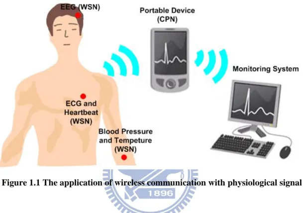
Figure 1.1 The application of wireless communication with physiological signal
With the economy growth, eating habit and life style of Taiwanese people are changed. Cardiovascular disease has increasingly youth-oriented tendencies. The wide range of types of cardiovascular disease includes Hypertension, heart failure, stroke and so on. And obesity, high cholesterol, and sedentary lifestyle are leading to an important risk factor for cardiovascular disease. Thus long-term electrocardiography (ECG) follow-up and medical analysis for patients suffering from cardiovascular disease is very urgent.
In the past, the way to measure ECG is that patient lies down on the bed to do a resting ECG. But arrhythmia doesn’t occur at any time. Thus Holter monitor system is necessary. It can detect the status of patient anytime.
2
communication, the application of wireless communication with the text and voice information moves toward a wider verity of applications. Used in the medical engineering, it can always transmit the patient’s physiological signals to the monitoring system to do 24 hours continuous record. Physiological signal is diverse including ECG, electroencephalogram (EEG), electromyography (EMG), body temperature monitoring, blood pressure and so on. Comparing with traditional wire transmission, it’s more convenient, high efficiency, portable, and low cost. All the physiological signals are connected to the monitoring system and recorded continuously via the wireless transmission. Allowing the doctor to get the more detail as the best basis for diagnosis.
In this application, low power is one of the key-point. Today many of the communication systems transforms the digital signal to baseband analog signal, a digital-to-analog interface is required. This interface allows the digital signal to analog signal transmitted through RF circuit and antenna out. Among many types of CMOS DAC architecture, the switched-capacitor circuit is the feasible low-power architecture. The main power consumption is operational amplifier. And the power consumption won’t have growth exponentially with the resolution. Low-power small-area DACs with 10bit resolution and several tens of MS/s sampling rate are considered to be one of the significant components in battery-operated commercial applications.
In this research, it is expected to suppress the power consumption so as to use 1.0 V power supply in analog circuit. A 10-bit 20MS/s filp around DAC with reconstruction filter has been designed and implemented with standard UMC 90nm CMOS 1P9M process.
3
1.2 Thesis Organization
This thesis is organized into five chapters. In Chapter 1, this thesis is briefly introduced. Chapter 2 begins with the concepts of wireless body network and wireless body on chip. Then, the architecture of low power DAC is reviewed. The architecture of flip around DAC is described in detail. The architecture of flip around DAC with accuracy and speed requirement are pointed out.
Chapter 3 describes the architecture of proposed analog baseband circuit and the problem of track and hold circuit. And then each block of flip around DAC including the operational amplifier with common mode feedback circuit, the buffer, the capacitor network, and the clock generator are shown. Then, transistor level simulated results of each circuit are shown.
Chapter 4 shows the simulation results, including the chip layout, system simulation result, and measurement consideration. Following the simulation results for reconfigurable analog baseband circuit described in Chapter 3 and fabricated in a standard UMC 90nm CMOS technology are summarized.
The conclusions of this work are summarized in Chapter 5. Following additional areas of researches are suggested and recommendations for the future work.
4
CHAPTER 2
OVERVIEW OF WIBOC BASEBAND
2.1 Introduction
In this chapter, the first describes the application of wireless body area network (WBAN) and the introduction of wireless body on chip (WiBoC). The second reviews some feasible low power digital-to-analog converter (DAC) architectures, including R-2R resistor ladder DAC, capacitive divider DAC, capacitive MDAC and flip around DAC. The fundamental issues in this design will be reviewed. The third focuses on key building blocks in flip around digital-to-analog converters. The specification of constraints and several techniques including of double sampling are discussed.
2.1.1 Introduction of WBAN
With economy growth, the average life expectancy in Taiwan has been growing. Taiwanese are living longer than ever with the average life expectancy reaching 79 years in 2010. But eating habit and life style of Taiwanese people are changed such as eating more, working over pressures, and living intensely and so on. Cardiovascular disease has increasingly youth-oriented tendencies. The potential factors of cardiovascular disease include stroke, high blood pressure, dyslipidemia, overweight, and diabetes mellitus, etc. These kinds of patents also have increasingly tendencies. The long-term electrocardiography follow-up and medical analysis for patients suffering from cardiovascular disease is very urgent. In the future, it will have a huge commercial opportunity.
5
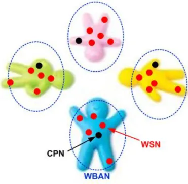
Wireless body area network (WBAN) is suitable for this kind of application. By disposing the sensors on human body and detecting the variation of physiological signal for a long time, it is an easy way to control the chronic diseases and unexpected accident. Such a lot of wireless sensor nodes (WSNs) and a central processing node (CPN) will form the body area network (BAN) around the human body. In the future, we can use this kind of technique to some applications. Through the wireless transmission of health information can not only improve the healthcare quality but also reduce the waste of medical resources. Figure 2.1 shows the basic topology of WBAN. Governments have been focusing on investing research-and-design in the building of electronic medical with wireless transmission.
Figure 2.1 Topology of WBAN
2.1.2 Introduction of WiBoC
Some research teams have adopted technologies such as, Bluetooth, ZigBee, GPRS to realize the medical systems of the remote ECG. However, since these
6
statements and standards were not purposely designed for applications of body area network, they cannot reduce power consumption efficiently. In addition, all elements around human body need to be taken into consideration so as to expand the application range of electronic health care system with wireless transmission. In 2006, IEEE 802.15 working group sets up relative specifications of WBAN. At that time, the system architecture meet the specification of WBAN were plotted synchronously, developed the low power transmission technique which can support 10 to 1Mbps, and named this wireless system as WiBoC (wireless body on chip). The establishments of platform and the chip of WiBoC can combine all sorts of sensors with portable mobile device (PMD) and provide long-term biomedical sensing, and then push forward services of chip, communication, and health screening service, thus create much more commercial opportunities. WiBoC includes system specification and hardware design as shown below.
1.) Wireless body on chip – system protocol (WIBOCS) 2.) Wireless body on chip – hardware architecture (WIBOCH)
Building the transmission of wireless sensor node (WSN) to central processing node (CPN) is the key point. WSN will be a miniature sensor used in wireless transmission system. It can be attached to various part of the body. Thus low power consumption is necessary. CPN is the personal portable data center. It can coordinate a number of WSN protocol on the body and collect data from WSN.
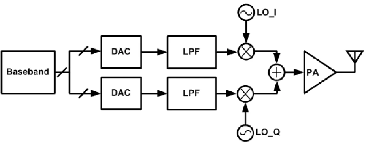
The wireless transmission system of WSN is shown in Figure2.2. The digital signal sent out from the baseband circuit is converted to baseband analog signal by the digital-to-analog circuit (DAC) and the low pass filter (LPF) and then this baseband analog signal is converted to radio frequency signal by mixer and local oscillator (LO). Finally, it sends out through the power amplifier (PA) and antenna.
7
Figure 2.2 The block of WSN system
The block of CPN is shown in Figure2.3. We need a low noise amplifier (LNA) to enhance the weak RF signal from antenna. LO with orthogonal phase output and two mixers turns this RF signal into two path baseband signals. VGA and LPF will amplify the baseband signal and remove the in-band noise. Finally, ADC turns baseband signal into digital signal and then baseband circuit processes these digital signal. The power consumption of CPN isn’t as harsh as WSN.
LNA VGA + LPF VGA + LPF ADC ADC Baseband Clock Gen LO_I LO_Q
Figure 2.3 The block of CPN system
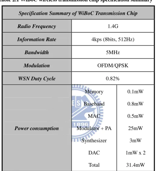
To save the battery life time, low power consumption is the key-point. WiBoC wireless transmission chip specification is shown in Table 2.1. The sampling
8
frequency of DAC is 20MHz, and the maximum DAC output frequency is 5MHz. Next, we show the possible low-power architecture used in WSN system.
Table 2.1 WiBoC wireless transmission chip specification summary Specification Summary of WiBoC Transmission Chip Radio Frequency 1.4G
Information Rate 4kps (8bits, 512Hz)
Bandwidth 5MHz Modulation OFDM/QPSK WSN Duty Cycle 0.82% Power consumption Memory Baseband MAC Modulator + PA Synthesizer DAC Total 0.1mW 0.8mW 0.5mW 25mW 3mW 1mW x 2 31.4mW
2.2 Review of DAC Architecture
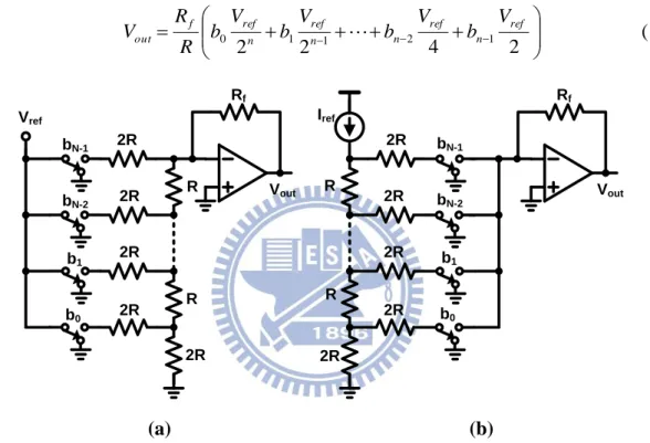
2.2.1 R-2R Resistor Ladder DAC
A simple way to implement low power DAC is R-2R resistor ladder. There are two kind of the architecture of the R-2R resistor ladder DAC. One is the voltage mode, another is the current mode. The voltage mode is using the principle of voltage
9
division to generate the relative voltage value at output node. And the current mode is using the principle of current division to produce the relative voltage across the resistor. There is a little difference between two architectures. Figure 2.4 shows the architecture of voltage and current mode R-2R resistor ladder respectively. For n-bits, according to the superposition the output of voltage mode R-2R resistor ladder DAC is 2 4 2 2 1 1 2 1 0 ref n ref n n ref n ref f out V b V b V b V b R R V (1) Iref 2R 2R 2R 2R 2R R R Rf Vout Vref 2R 2R 2R 2R 2R R R Rf Vout bN-1 bN-2 b1 b0 bN-1 bN-2 b1 b0 (a) (b)
Figure 2.4 (a) Voltage mode R-2R resistor ladder DAC (b) Current mode R-2R resistor ladder DAC
We must consider the magnitude of the resistor in case it affects the gain of the operational amplifier. Either voltage or current mode architecture, the disadvantage of the R-2R resistor ladder is that input-output characteristic isn’t intrinsically monotonic. As the switch is turned on, the effective resistance value will exist. This turn on resistance will cause negative effect on overall efficiency of DAC. The worst case will occur at the mid-point.
10
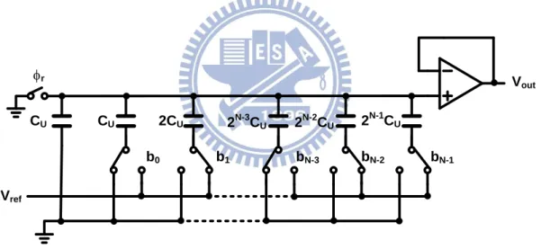
2.2.2 Capacitive Divider DAC
An example of a capacitive divider DAC with output buffer is shown in Figure 2.5. It’s the binary weighted architecture. In the reset phase, all of the capacitors are discharged with digital at 0. In the conversion phase, the reset switch is opened and the capacitors are connected to reference voltage or ground depending on the digital control code. Any resistance loading at the output node will absorb the charge stored on the capacitors. Thus the capacitor based DAC needs to avoid discharging at the output node. An output buffer with infinite input resistance is necessary. The voltage swing of the DAC is limited by the buffer input or output stage.
CU CU 2CU 2 N-1 CU 2N-3CU 2N-2CU Vref Vout bN-1 bN-2 bN-3 b1 b0 fr
Figure 2.5 N-bit Capacitive divider DAC
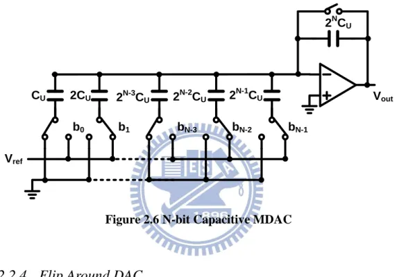
2.2.3 Capacitive MDAC
The output buffer used in n-bit capacitive divider DAC has to ensure that the input dynamic range equals to reference interval with high linearity. It’s not easy for many kinds of operational amplifiers. The capacitive MDAC shown in Figure 2.6 is a solution which can overcome these issues. The value of the feedback capacitor
11
depends on the required gain of the conversion. In this example, a gain of 1 is obtained. In the reset phase, the input and feedback capacitors are discharged. In the complementary phase of the reset phase, the capacitors are connected to reference voltage or ground depending on the digital input code. The charge current flows through the feedback capacitor and forms the output voltage across the feedback capacitor. CU 2CU 2N-2CU 2N-1CU Vref Vout 2NCU 2N-3CU bN-1 bN-2 bN-3 b1 b0
Figure 2.6 N-bit Capacitive MDAC
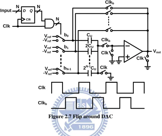
2.2.4 Flip Around DAC
The capacitive MDAC uses 2(2N-1) unity capacitors. The number of the unity capacitor will increase exponentially with the number of bits. These large number of capacitors will occupy quite area. Comparing with flip around DAC, it just needs a half the number of capacitors of the capacitive MDAC. Figure 2.7 shows the architecture of flip around DAC with differential operation. When Clk=1, it is in the sampling mode. All the sampling capacitors are connected to corresponding reference voltage depending on the digital control code and operational amplifier resets its input and output to common mode voltage. When Clkb=1, it is in the hold mode. All of the
12
sampling capacitors are tied together and connected to the output of operational amplifier. By charge sharing and parallel connection, the corresponding output is shown. 2CU CU -Vref -Vref Vref Vref Clk Clkb Clkb -Vref Vref Vout Clk b0 b1 bN-1 D Input Clk N N Q Clk N Clk Clkb Clk 2N-1CU
Figure 2.7 Flip around DAC
The flip around DAC consumes less power consumption than capacitive MDAC because of two features. Firstly, during the hold mode the operational amplifier doesn’t charge the capacitor. Because of the sampled charge is only shared between all of the sampling capacitors during the hold mode. Thus amplifier of flip around DAC consumes less power consumption than the amplifier of the capacitive MDAC. Secondly, the feedback factor from output node to input node is 1. In contrast with capacitive MDAC assumed with a gain of 1 is the middle node of the two serial capacitors. Thus the feedback factor is 0.5. The feedback factor will affect operational speed during the hold mode. The bigger feedback fact has the shorter settling time. Table 2.2 summarizes the comparison with different DAC architecture.
13
Table 2.2 Architecture comparison
Specification R-2R ladder Capacitive
divider MDAC Flip around
Resolution (bits) ~10 ~10 ~ 10 ~ 10
Sampling Rate Low Low Low Low
Power
Consumption Medium Small Small Small Active Area Medium Medium Large Medium
Disadvantage Input-output characteristic isn’t intrinsically monotonic Voltage swing is limited by buffer Capacitor network occupies large area Speed is limited by operational amplifier
2.3 Design Issue of Flip-Around DAC
2.3.1 Return-to-zero DAC
Dynamic nonlinearity in the DAC output response is an issue which must be concerned. By Fourier transform, the whole value of the DAC in the time domain can transforms to its frequency domain representation. Thus any non-ideal response in the time domain will relatively form any spur level in the frequency domain. One conceptual solution to the dynamic linearity problem is to eliminate the dynamic nonlinearities of the DAC.
Figure 2.8 (a) and (b) show the flip around DAC in the sample mode and hold mode respectively. In the sample mode, operating amplifier is floating. In the hold mode, the corresponding output is shown. Thus it needs a sample-and-hold (SAH) circuit at the DAC output to hold the output value in the sample mode. Figure 2.9(a) shows the one of the simplest realizations of SAH circuit composed of an input buffer, a hold capacitor, and an output buffer. The hold capacitor is switched to the input
14
buffer in the sample phase and disconnected in the hold phase. The circuit not only consumes extra power consumption but also suffers from a number of drawbacks with respect to dynamic linearity.
(a) (b ) Figure 2.8 the conversion of flip around DAC (a) sample mode (b) hold mode
Figure 2.9(b) shows the problem of SAH circuit. Firstly, the track-to-hold step (number 1 in figure) will limit the performance. When the switch changes from track to hold, the pedestal error in the output voltage is incurred. In order to reduce the turn on resistance, it must enlarge the width of switch. This behavior leads to deepening the impact of pedestal error. Or we can increase the hold capacitor, CH, to inhibit the pedestal error. But it will enlarge the output loading of the amplifier. The closed-loop architecture minimizes this error by keeping the input of the buffer at virtual ground. The second performance limitation is formed by the droop rate (number 2 in figure). Any nonzero input current of buffer will absorb the charge stored on the capacitors. The third limitation is formed by the hold mode feedthrough (number 3 in figure). During the hold mode, a parasitic capacitor from the input node to the output node of the switch will cause the feedthrough of the input signal to the hold capacitor. Even if this transfer function is signal independent, it introduces a non-linearity. Finally, this
15
architecture suffers from track mode error (number 4 in figure). It involves nonlinear settling behavior of the buffer mainly. For the open loop case, the nonlinearity is due to signal dependence of the bias current, nonlinear device output resistance, and nonlinear transconductance transfer functions. These drawbacks will eliminate the dynamic nonlinearities of the DAC. Using the return-to-zero (RZ) scheme at the DAC output is the way to improve the DAC dynamic performance [5], [8], [9].
(2),(3) (1) Input Buffer Output Buffer CH CH In Out (4) (a) (b) Figure 2.9 (a) SAH architecture (b) problem of SAH circuit
The comparison of time- and frequency-domain of conventional full-wave DAC and RZ DAC is shown in Figure 2.10, where in is the sinusoid input signal to DAC with magnitude T and s is the sampling frequency. From the time domain waveform, quantized signal of conventional DAC is twice longer than RZ DAC. Comparing with conventional DAC, in the frequency domain it halves its magnitude but doubles the sampling frequency when using RZ DAC. Therefore, in the pass-band RZ DAC has less output signal power and sinc-1 distortion than conventional DAC. At half the sampling frequency, in the case of conventional DAC the magnitude of sinc-1 function rises to 3.9dB. In the case of RZ DAC, the magnitude of sinc-1 function only rise to
16
0.9dB. The envelope of the RZ DAC makes less distortion and allows the sinc-1 filter to be eliminated [12], [16]. t Conventional DAC t Retuen-to-Zero DAC s -s -2s 2s s -s -2s 2s Envelope : T sinc(T/2) Envelope : T/2 sinc(T/4) in -in in -in
Figure 2.10 Time and frequency domain comparison
2.3.2 Accuracy and Speed Requirement
The operational amplifier used in DAC plays an important role. The bandwidth of operation amplifier will limit how fast the circuit can operate. The gain and offset will affect how accurate the DAC output value. In many applications, DAC will concern different non-linearity effects. For example, monitor driver IC will concern the static specifications. But now it’s applied to transmitter so we won’t care about the gain error and offset error because they won’t affect the linearity, that’s to say, it won’t cause the 3-rd harmonic tone to rise up even if there are gain error and offset error.
17
switched-capacitor technique. In the switched-capacitor circuit, operational amplifier is the one of the most important component. It can dominate the speed and precision issues. Right now we must consider the accuracy and speed requirement individually.
First of all, we consider the accuracy requirement. During the operation, the operational amplifier gain isn’t constant. Thus it generates the nonlinearity term. Suppose the open-loop input-output static characteristic of operational amplifier can be approximated by a fifth-order polynomial [15] such as
5 out 5 4 out 4 3 out 3 2 out 2 out 1 in a V a V a V a V a V V (2) Approximating the inverse function by a fifth-order polynomial as
5 in 5 4 in 4 3 in 3 2 in 2 in 1 out b V b V b V b V b V V (3) Substituting equation (2) into (3) and equating the like powers, it follows that
1 5 4 3 2 1 1 1 a 1 a , a , a , a , a f b (4)
3 1 2 5 4 3 2 1 2 2 a a a , a , a , a , a f b (5)
5 1 2 2 3 1 5 4 3 2 1 3 3 a a 2 a a a , a , a , a , a f b (6)
7 1 3 2 3 2 1 2 1 4 5 4 3 2 1 4 4 a a 5 a a a 5 a a a , a , a , a , a f b (7)
9 1 4 2 3 2 2 1 2 3 2 1 5 3 1 4 2 2 1 5 4 3 2 1 5 5 a a 14 a a a 21 a a 3 a a a a a 6 a , a , a , a , a f b (8)18
We apply the above equations to flip-around DAC, shown in Figure 2.11, employing such an operational amplifier. Cp is the equivalent parasitic capacitor. In the flip-around architecture, the conversion from sample mode to hold mode yields
i f
o a
p a f V C V V C VC (9) Rearranging the equation (9) gives
a o f p f a o i V V C C C V V V (10)
where Va is the input of operational amplifier. Substituting for Va from (2) gives
5 5 4 4 3 3 2 2 1 1 o o o o o i V a V a V a V a V a V (12) According to equation (3), the inverse function of equation (12) is
5 5 4 4 3 3 2 2 1 in in in in in o cV c V cV c V c V V (13) Thus, the closed-loop input-output characteristic with operational amplifier nonlinearity is obtained. Using the equation (4) to (8), the parameters of equation (13) is calculated. Thus, the effect of high order tones caused by operational amplifier nonlinearity can be verified in software simulation.
19
About the speed requirement, we must consider the output slewing and settling. Figure 2.12 shows the plot of output slewing and settling. In the sample mode, each sampling capacitors are charged. When switch to the hold mode instantly, Va equals to –Vref+ and Vb equals to –Vref- as shown in Figure 2.13. When Va Vb 2Vov,
it’s during slewing. At this time, the output voltage and settling time are
ref ov
settle 2V 2V V (14) I V Ctsettle load settle (15)
(a) (b) Figure 2.13 DAC operation (a) sample mode (b) hold mode
When VaVb 2Vov, it’s during settling. The closed-loop step response is
t tslew
settle slew o t V V 1 e V (16) t 1 (17)where is the settling time constant. Since the settling error is
N tsettle e 2 2 1 (18)
where tsettle is the time interval of the settling of operational amplifier and N is the number of the resolution of the next stage. Rearranging terms gives
settle t t N f 1 ln2 2 1 (19)20
According to above equation, we can determine the required unit-gain frequency to meet the constraints.
2.3.3 Estimation of Thermal Noise in Switched-Capacitor Circuit
Noise is the one of the main limitations which limits the performance of the switched-capacitor. In general, there are two intrinsic noises in MOS transistor: thermal noise and flicker noise.
Thermal noise is caused by the fluctuations of the random motion of electrons in the channel of the device introduced into the voltage even if the average current is zero. This fluctuation will form a small amount of drain current. Namely the thermal noise can be modeled as a current source in parallel with the channel. An approximation of the PSD of the thermal noise current is given by
m T i kTg S 3 8 , (20)
where k1.381023J K is the Boltzmann constant, T is the absolute temperature in degrees Kelvin, and gm is the transconductance of the device. Note that Si,T is expressed in V2/Hz. The mean value of the thermal noise is zero. All of the PSDs are generated by one-sided distribution.
Flicker noise is caused by charge carriers getting trapped and released randomly by energy states. It is more easily modeled as a voltage source connecting to the gate and approximately given by
WLf K
Sv,f (21)
where K is the process dependent parameter, W and L are the width and length of the channel, and f is the frequency. At high frequency most of noise power is decayed. Using large input devices and choosing pMOS rather than nMOS also can reduce the
21
flicker noise. Thus we just consider the effect of thermal noise on the performance of SC circuit. The noise is contributed by these sampling switches and the CMOS operational amplifier. Here assuming all of the noise voltages are uncorrelated.
R1 C1 R0 Ron C1 2 n
V
2 1 , nV
2 0 , nV
+ VC1 (a) (b) R1 R2 R9 R10 C1 C2 C9 C10 2 1 , nV
2 2 , nV
2 9 , nV
2 10 , nV
(c) Figure 2.14 Noise analyzing in the sample phaseAbout the noise introduced by switches, we can use the equivalent circuit combined with noise source to find the noise voltage across C1 in the sample mode. As shown in the Figure 2.14(a), the conducting switches are replaced by noise voltage
22
and turn-on resistance individually. It can be simplified further as one equivalent noise source shown in Figure 2.14(b). The Ron is the combined equivalent resistance and the PSD of the Vn is
on R V kTR S on 4 , (22)
We compute the transfer function from VC1 to Vn
1 1 1 1 1 C sR V V s H on n C (23)With transfer function in equation (22) and (23), the PSD of the noise voltage across C1 can be expressed as
2 1 , 2 1 , 1 , 2 1 1 2 C fR j S f j H S f S on R V R V C V (24)Integrating for all frequency from 0 to infinite, we can get the total mean-square power
1 0 , 1 1 C kT df f S PC
VC (25) where is independent of Ron. From equation (25), we can obtain the noise charge stored on C1 as 1 1 2 1 2 1 C P kTC QC C (26)The charge-redistribution DAC will have several input branch. In the sample mode, all of the uncorrelated noise voltages are stored on Ci individually, as shown in Figure 2.14(c). With the equation (25) and (26), we can obtain the total noise charges stored on sampling capacitor as
10 1 10 1 0 , 2 2 2 2 i i i Ci V i i C C H j f S df kTC Q (27)where Hi
j2f
is the transfer function form the ith noise source to the output andCi V
23
will form an output-referred noise power
2 10 1 2 2 ,
i i C C O C Q P (28)Dividing the closed loop gain G, the total input-referred noise power from sampling switches is given by 2 2 , 2 , G P PnC OC (29)
In the SC circuit, the noise of operational amplifier will provide the significant capacity. It’s the necessity of estimating the effect of the noise in the operational amplifier contributed to SC circuit. First we concern the total output noise current of the operational amplifier. In general, the PSD of the noise current at the output of the operational amplifier is m noise op F kT g I 3 2 4 2 , (30)
where F is dependent on the architecture of the operational amplifier. The operational amplifier will just have function in the hold mode. Thus the equivalent capacitive feedback with operational amplifier is shown in Figure 2.15.
C
pC
fC
Lr
oG
mV
a+
V
a-
op noiseI
,V
oFigure 2.15 The noise model of operational amplifier
24
more familiar current quantity. The transfer function of Vo to Iop,noise is
f p f o m o T f p f o m o noise op o C C C r g r sC C C C r g r I V s T 1 1 1 , (31) where p f p f L T C C C C C C (32)The total output noise power is determined by calculating the total area under the spectral density, so that
s I d T Poop opnoise 2 , 2 0 ,
(33) For a one-pole system, the noise bandwidth is equal to /2 times the pole frequency. Therefore, rearranging equation (33) and multiplying the equivalent noise bandwidth gives 2 1 1 2 3 2 4 1 2 , o T f p f o m m f p f o m o op o r C C C C r g g kT F C C C r g r P (34)For large ro, this expression reduces to
T T f p f op o C kT F C C C C kT F P 1 3 2 3 2 , (35)
According to equation (35), we can get the equivalent input noise of the closed-loop circuit contributed by op-amp, that is
T op o op n C kT F G P P 3 2 2 , , (36)
25
contributed by switches and operational amplifier is the square of LSB/4. With equation (29) and (36),
dB dB N LSB LSB LSB P P P P SNDR N op n C n quan signal 43 . 2 76 . 1 02 . 6 4 12 2 2 2 log 10 log 10 2 2 2 , , (37)If the upper limit of the noise power is lower than LSB/4, the noise contributed to SNDR is smaller. All of the relevant parameters can be substituted into the equation (29), (36) and (37) to see if there is to meet the noise requirements [4].
2.3.4 Double Sampling
In the sample phase, sampling capacitors are connected to reference voltage or ground. The operational amplifier just reset to common mode voltage but it still has power consumption. We can build another duplicate path to let the amplifier is always in hold conversion. This way is named as double sampling. By this way, output data rate is doubled without extra power consumption. We can separate the doubled output data into two DACs. It doesn’t have the timing skew and gain mismatch issues. But it still has memory effect.
Due to the finite gain of the operational amplifier, a fraction of the previous sample remains in the input parasitic capacitance of the operational amplifier. In the hold mode, every output is affected by the finite-gain error component from previous remained charge. This phenomenon is called memory effect. It can be suppressed by proper circuit design.
26
CHAPTER 3
FLIP AROUND RETURN-TO-ZERO DAC
3.1 Flip Around DAC Design
In this chapter, the first introduces the architecture of proposed analog baseband circuit, and describes the problem of track-and-hold circuit and the characteristic of return-to-zero DAC. The second focus on each block of flip around DAC. Finally, the third is the filter design.
3.1.1 System Architecture
The static performance of DAC is characterized by integral nonlinearity (INL) and differential nonlinearity (DNL). The dynamic performance of DAC is its spectral purity, i.e., the level of spurious frequency components present in the DAC output. In general, spur in the output spectrum is related to the input signal harmonically. It is also generated due to dynamic nonlinearities in the DAC output response. Spectral purity is required because these spurs have the information content of the DAC output signal. Typically, it’s measured by means of its spurious-free dynamic range (SFDR).
Spur related to the input signal harmonically is resolvable. If spur related to the input signal is even, we will guess that the whole symmetry isn’t well. If spur related to the input is odd, we will confirm that there is the existence of the nonlinearity. We can try to find any possible case caused nonlinearity out and fix it.
Dynamic nonlinearity in the DAC output response is an issue which must be concerned. By Fourier transform, the whole value of the DAC in the time domain can
27
transforms to its frequency domain representation. Thus any non-ideal response in the time domain will relatively form any spur level in the frequency domain. The proposed analog baseband circuit can decrease any non-ideal response in the time domain. The whole circuit architecture is shown in Figure 3.1 including DAC, buffer, and low-pass filter (LPF). It is a return-to-zero DAC. The sixth-order Butterworth LPF removes the out-of-band residual quantization noise and suppresses the DAC spectral images. 2C C 512C D Input CLK1 10 10 CLK1 CLK2 CLK2 Q Clk 10 CLKr Output LPF DAC CLKd2 CLKd2_b CLKr CLK1 CLK2 CLKd2 CLKr CLKd2_b Buffer -Vref -Vref Vref Vref -Vref Vref
Figure 3.1 Architecture of proposed analog baseband circuit
When CLK1 is high, all of the sampling capacitors are connected to corresponding reference voltage depending on the digital control code. The delay cell connected at the AND logic output is to perform the bottom plate sampling. When CLK2 is high, all of the sampling capacitors are tied together and connected to the output of operational amplifier. The corresponding output is shown by charge sharing.
28
In the hold mode, due to the finite bandwidth of the amplifier, it needs a certain time to settle the output. The impact of this factor present in the DAC output will limit the overall circuit linearity. Therefore, for the charge redistribution DAC, operational amplifier will severely limit the speed and linearity of the DAC. This kind of architecture makes the speed of the DAC is not quick. In order to overcome this problem, we use additional clock phase, CLKd2, to control the switch connected to the buffer. This clock phase is intended to stop the impact generated by amplifier. Within a certain period of time, the output of amplifier must be settled. The switch which is controlled by CLKd2 is turned on, and then the DAC output is transferred to the buffer. When the complementary phase of CLKd2 is high, the buffer input is connected to common mode voltage. The diagram plotted in Figure 3.2 shows the waveform of DAC output. Through this method, it can effectively generate a waveform similar to ideal RZ DAC. Finally, through the reconstruction filter the smooth analog signal is constructed. The duty cycle of CLKd2 is a little smaller than CLK2. The phase difference between two clocks determines the bandwidth requirement of the amplifier. In this architecture, we design that the output of amplifier is settled within 3 nanoseconds. DAC Output Time Output of Ideal Return-To-Zero DAC Output of Actual Return-To-Zero DAC Output of Proposed Return-To-Zero DAC
29
3.2 Each Block of Flip Around DAC
3.2.1 Capacitor Network
The linearity of the flip around DAC is dependent on the capacitor matching in capacitor array. There are several causes will make the capacitor ratio error. The undercutting of the mask which defines the capacitor is the one of them. During the etching phase of the photomask process, a poorly controlled lateral etching is called undercut. This problem can be done by paralleling identical size unit capacitor to form the large capacitors. By this way, the effect of undercutting is greatly restrained.
(a) (b) Figure 3.3 Shielding capacitor (a) top view (b) cross sectional view
In general, the unit capacitor used in binary weighted architecture is metal-insulator-metal (MIM) and poly-insulator-poly (PIP). MIM is a parallel-plate capacitor formed by two planes of metal separated by a thin dielectric. And PIP is also a parallel-plate capacitor which is formed between POLY1 and POLY2. In process both of them will need extra mask so it costs a lot of money. The shielding capacitor is shown in Figure 3.3. The gray part is the top plate which is enclosed by the bottom
30
plate to minimize the parasitic capacitor. By using three metal layers to construct a unit capacitor, it produces better matching characteristic without extra cost. The size of the unit sandwich capacitor is 3.3m3.7m and the capacitance of the unit sandwich capacitor is 1.86fF. In the manufacturing process, there is no doping. We can assume the asymmetry between each capacitor is random. Thus the effect caused by gradient is neglected [10], [11].
Figure 3.4 Parallel plate capacitor
The shielding capacitor is composed of two layers metal and oxide. We can use the parallel plate capacitor model to explore the capacitor matching. Figure 3.4 shows the parallel plate capacitor. The difference between two shielding capacitor is normally distributed with zero mean. The standard deviation is
WL A C C C (38) where AC is the area proportionality constant for parameter C. Proportional
relationship can be used to obtain the standard deviation between two shielding
capacitors. It gives unit MOM unit MOM MOM MOM C C WL WL (39) The standard deviation of asymmetric MOM capacitor (47fF) is 0.1%. Substituting
31
MOM into equation (39) and rearranging the equation gives % 486 . 0 f 86 . 1 p 1 MOM unit (40)
Let standard deviation of unit capacitor is 0.5%. Two groups of 1023 unit capacitors are generated randomly with 0.5% standard deviation. And then these unit capacitors form two groups of binary weighted capacitors to simulate the flip around DAC operation. The digital codes represented 5.01MHz signal at 20MHz sampling frequency control two groups of binary weighted capacitors to produce the corresponding output value. After running 1000 times, the statistic of the range of SFDR and SNDR are plotted as probability density function (PDF) and cumulative distribution function (CDF). Figure 3.5 and 3.6 show the case of SFDR and SNDR respectively. Under both figures, we can see the distribution of performance. The probability of SFDR higher than 68 dB and SNDR higher than 60dB is over 90%.
(a) (b) Figure 3.5 SFDR (a) PDF (b) CDF
32
(a) (b) Figure 3.6 SNDR (a) PDF (b) CDF
The layout of the capacitors must make sure that the wire connected every capacitor to the output terminal has the same binary weighted value. This is required to maintain an accurate binary weighting of this network. The problem of parasitic capacitance caused by the layout routing is shown in Figure 3.7. Assume that the route is from the bottom of the capacitor. The layout routing around the other unit capacitors will produce extra parasitic capacitances. These parasitic capacitances of the layout routing will be attached to the unit capacitor so as to affect the linearity, common centroid method especially. It has the complex layout routing. In order to reduce the impact of the parasitic capacitor caused by the layout routing, we will enlarge the distance between each unit capacitor. And then it occupies a lot of area.
The layout floor plan of capacitor network is shown in Figure 3.8. It’s different from common centroid structure. It can avoid any routing inside the capacitor array. Therefore the parasitic capacitor caused by the layout routing is minimized. The dummy array outside the matrix is placed to obtain the maximum matching accuracy. The top-plate of the sampling capacitors is connected to the amplifier input.
33 Cp Cp Cp Cp Cp Cp Cp Cp Cp Cp Cp
Figure 3.7 Parasitic capacitance caused by the layout routing
34
3.2.2 Operational amplifier and Common Mode Feedback Circuit
The schematic of differential operational amplifier used in DAC is shown in Figure 3.9. M1-M5 composes the simplest one stage differential operational amplifier which has the best bandwidth performance. But it can’t support high gain performance. In order to eliminate the operational amplifier nonlinearity, the high gain operational amplifier is necessary. But the effect of operational amplifier nonlinearity doesn’t exceed the quantization noise, it’s not dominant. As long as the operational amplifier nonlinearity is good enough to maintain the certain resolution, low gain isn’t an issue. It just affects the slope of transfer function of digital code to corresponding output.
Figure 3.9 Operational amplifier with CMFB used in DAC
Common mode feedback circuit (CMFB) can sense the common mode level of the differential outputs and adjust one of the bias currents in the amplifier. In general case, it has been preferred to use switched-capacitor based CMFB circuit for switched-capacitor application. Switched-capacitor CMFB circuit doesn’t consume significant power. But it will contribute extra significant output loading. Thus the
35
operational amplifier need more power to maintain the speed requirement. And large capacitor will occupy considerable area.
Here we choose to use the continuous time CMFB instead of switched-capacitor based CMFB. As shown in Figure 3.9, M6-M10 and R1-R2 compose to CMFB. The CM level depends on how close ID4 and ID5 to ID1/2 so it is quite sensitive to device properties and mismatches. R1 and R2 compose the CM level sense circuit which detects the two outputs and specifies the according CM level at node OutCM. M6-M10 composes the simple amplifier to sense the difference between OutCM and VCM, and to adjust ID4 and ID5 so that the CM level equal to VCM as close as possible. This CMFB needs a small amount of power consumption. Comparing with switched-capacitor based CMFB, it has lower power consumption. The disadvantage of the CMFB circuit is that R1 and R2 must be greater than the output resistance of operational amplifier lest the open loop gain is lower. In the high-gain operational amplifier output impedance is higher 100k, necessitating a value of around mega-ohms for R1 and R2. Such large resistance will occupy a large area and produce a considerable parasitic capacitance.
Figure 3.10 shows the gain under different output swing in three corners. It can be predicted that there will be the worst case in the FF corner. Now, we explore the effect of operational amplifier nonlinearity. First, the open-loop input-output characteristic of the operational amplifier can be fitted by a fifth-order polynomial. Figure 3.11(a) and (b) plot the input-output characteristic and the inverse function of equation (3). One curve is the real operational amplifier. Another is the fifth-order polynomial. Obviously, fifth-order polynomial fits the real operational amplifier across the voltage range of interest. When the output range is between ±300mV, two curves are almost the same. We can use this fifth order polynomial to represent the
36
actual operational amplifier, and explore the impact on the overall performance under the closed loop.
Figure 3.10 output swing versus gain
(a) (b) Figure 3.11 Operational amplifier (a) Input-output characteristic (b) inverse
function
Equation (13) is the closed-loop input-output characteristic of flip around DAC. The parameters, c1 to c5, can be evaluated in software. As shown in Figure 3.12, a 5.01MHz sinusoid is fed into the closed-loop transfer function to observe the output resolution. Figure 3.13 shows the SFDR under the different amplitude in three corners.
37
Suppose the effect caused by capacitor matching is below the quantization noise. When amplitude is greater than 0.15V, operational amplifier nonlinearity will possibly dominate the SFDR in FF corner.
Vi 5 i5 4 i 4 3 i 3 2 i 2 i 1 o cV c V cV c V c V V Vo Fin=5.01MHz
Figure 3.12 Block diagram of sinusoid signal feds into the equivalent function
Figure 3.13 SFDR versus output swing with 5.01MHz sinusoid input
In Table 3.1, post-simulation results are shown. The gain of operational amplifier is around 25dB in different corner. Now choosing total 10 bit resolution to calculate the specification about speed. The output loading is about 700 femtofarad and the feedback factor is 0.97. Substituting into equation (15), the slewing time is near 0.3 nanoseconds when reference voltage is 0.15V. Assuming in 3 nanoseconds, the speed requirement will reach 10 bit resolution within the error range. Subtracting the
38
slewing time and substituting into equation (19), we can get more than 463MHz bandwidth of operational amplifier required to achieve.
Table 3.1 Operational amplifier post-simulation results
Supply Voltage 1V
Input and output common mode voltage 0.45V , 0.6V
Output Loading 0.7pF
Differential Output Range 600mVPP
Post-simulation Corner TT SS FF DC Gain A0 [dB] 25.03 25.16 24.9 Unity-Gain Frequency fu [MHz] 528 507.77 548.62 Phase Margin [°] 89.6 89.42 89.8 Power Consuption [W] 359 351 367
3.2.3 Source Follower
The buffer is connected at the DAC output and drives the reconstruction filter. The buffer used in the stage is the source follower as shown in Figure 3.14. The advantage of source follower is the largest bandwidth. Many nonlinear terms need to consider including signal dependence of the bias current, nonlinear device output resistance, and nonlinear transconductance transfer functions. Enlarging the length of the device and the drain-source voltage can enhance the output resistance so as to restrain the signal dependence of the bias current and nonlinear device output resistance. The change in the threshold voltage by the change in the source-bulk
39
voltage will form the nonlinear transonductance transfer function. Thus the source and bulk of M1 is connected to enhance the linearity.
Vin
Vout
Iref M1
M2
M3
Figure 3.14 Source follower with bias circuit
3.2.4 Double Sampling
By the duplicate circuit, using time interleave skill produces double the output throughput without extra power dissipation. Figure 3.15(a) and (b) mean the flip around DAC circuit during Clk1 and Clk2 respectively. When Clk1 is high, the capacitors CS0_1 to CS9_1 are sampled to reference voltage. The duplicate capacitors CS0_2 to CS9_2 are connected to the output of operational amplifier. When Clk2 is high, the duplicate capacitors CS0_1 to CS9_1 are sampled to reference voltage and CS0_1 to CS9_1 are connected to the output of operational amplifier.
By applying the technique, the amplifier is always in hold conversion. But, memory effect is induced as well. We need additional clock phase to reset the input and output of amplifier to common mode voltage. Therefore, add clock Clkr between Clk1 and Clk2 to cancel the memory effect. The Figure 3.15(c) shows that the input and output of amplifier resets to common mode voltage during Clkr. The clock waveform is shown in Figure 3.15(d).
40 Cs9_1 Cs0_1 Vref+ V ref-CLK1 Cs9_2 Cs0_2 Vout Cs9_2 Cs0_2 Vref+ V ref-CLK2 Cs9_1 Cs0_1 Vout (a) (b) Vout CLK2 CLK1 CLKr (c) (d) Figure 3.15 Double sampling
(a) During Clk1 (b) During Clk2 (c) During Clkr (d) Clock waveform
3.2.5 Clock Generator
Figure 3.16(a) and (b) show the clock generator schematic and waveform diagram respectively. The double sampling technique is used to multi-output application. There is no necessary to be aware of the complementary delay. By tuning the size of transmission gate, we can get the best situation which has least clock skew effect. Figure 3.16(c) shows the simulation result.
41 CLK_in CLK2 CLK1 CLKr CLKd1 CLKd2 (a) CLKr CLK1 CLK2 CLKd1 CLKd2 (b) CLKr CLK1 CLK2 CLKd1 CLKd2 Voltage[V] Time[sec] (c)
Figure 3.16 (a) clock generator schematic (b) waveform diagram (c) simulation resolutoin
42
3.3 Reconstruction Filter
3.3.1
Filter Architecture
The baseband filter is placed after the DAC to perform the signal reconstruction. The sampling frequency is 20MHz, and the maximum DAC output frequency is 5MHz. Such low oversampling rate will need higher order filter. Here we use the Here we use the sixth-order Butterworth filter to build reconstruction filter. The sixth-order Butterworth filter is based on active R-C architecture. Active R-C filter has better linearity. The transfer function of sixth-order Butterworth filter is
1 5179 . 0 1 1 4142 . 1 2 1 9319 . 1 2 2 2 2 3 2 1 s s s s s s s T s T s T s T (41)It’s composed of three single-amplifier biquad (SAB) filter as shown in Figure 3.17. The section order is chosen such that the section sequence is in the order of increasing value of Q. The section with the flattest magnitude of transfer function comes first, the next flattest one second, and so on. It’s very close to the optimum. The SAB filter design and the effect caused by real operational amplifier on SAB filters will be presented [13]. R1 R3 R2 C1 C2 Vin R1 R3 C1 C2 R2 R1 R3 R2 C1 C2 R1 R 3 C1 C2 R2 R1 R3 R2 C1 C2 R1 R3 C1 C2 R2 Vout
43
3.3.2
Single-amplifier biquad (SAB) filter
The structure of SAB filter used in reconstruction filter is shown in Figure 3.18. The voltage transfer function is given by
R1 R3 R2 C1 C2 Vin Vout
Figure 3.18 Low-pass single-amplifier biquad filter
The general form of the second-order low pass filter is described by
2 2 2 0 n n n in out s Q s H V V (42)
If the operational amplifier is ideal, the transfer function of Figure 3.18 is
1 2 1 1 1 3 1 2 1 3 1 2 1 1 1 1 2 1 2 1 1 1 3 1 1 C C R R R R R C s s C C R R V V in out (43) By comparing with equation (42),2 1 3 2 1 C C R R n (44) 1 2 0 R R H (45) 1 3 2 2 3 1 3 2 2 1 R R R R R R R C C Q (46) Assuming C1 CandC2 mC. Substituting these into equation (44), (45), and (46) gives 0 2 1 H R R (47)