The Design of Asynchronous Processor
25
0
0
全文
(2) The Design of Asynchronous Processor Chang-Jiu Chen, Chih-Chiang Shiu and Men-Shu Wu. Department of Computer Science and Information Engineering National Chiao Tung University. Abstract Asynchronous processors have become a new aspect of modern computer architecture research in these years. An asynchronous processor is by no means synchronized by global clock. However, it employs communication protocols doing synchronization instead. Basically, in contrast with synchronous processors, asynchronous processors possess certain advantages while definitely encounter new challenges. Therefore, we were interested in asynchronous processor, and we desired to design it thus. In this paper we design an asynchronous processor based on the MIPS R2000 instruction set architecture. Specifically, we accomplish the design of an asynchronous processor named Asynchronous MIPS (AMIPS), and it is implemented by SystemC. The SystemC is a hardware description language like Verilog, which contains C++ object-oriented features in it. Finally, we check the AMIPS by each and almost every instruction, and also test it by several programs coded by us. All of the results of these checks and tests match the expected functionality. Keywords: asynchronous circuit, asynchronous processor, AMIPS. 1.
(3) 1. Introduction The goal of this paper is to design an asynchronous processor. Firstly, the motivation of designing the asynchronous processor is depicted in this section. Then we introduce asynchronous processor by contradicting it with synchronous processor. Finally, it is the related work.. 1-1 Motivations Asynchronous architecture is a new research topic in computer architecture[4,7]. There are several asynchronous processor prototypes announced in the past years. Recently asynchronous architecture develops quickly and it solves the global clock and power dissipation problems. Asynchronous processor has the better performance and power dissipation in real world today. However, in the past, if we want to design the real chip, we must design the simulator first. Recently the design flow is changed by the Hardware Description Language (HDL) based on high-level language, like the SystemC[1,2]. SystemC is a high-level language based on C/C++. It provides the fast design flow and object-oriented HDL, which is useful to integrate the simulator and real chip design flow. SystemC is a C++ class library and a methodology that we can use to effectively create a cycle-accurate model of software algorithms and hardware architecture[1]. We can use SystemC and standard C++ development tools to create a system-level model, quickly simulate to validate and optimize the design, explore various algorithms, and provide the hardware and software development team with an executable specification of the system. SystemC supports hardware-software codesign and the description of the architecture of complex systems consisting of both hardware and software components. It supports the 2.
(4) description of hardware, software, and interfaces in a C++ environment. So we try to design an asynchronous processor based on the MIPS R2000[8] processor by using SystemC.. 1-2 Introduction to Asynchronous Processors All present computers are synchronous. They process instructions according to an internal timing device that regulates processing. The synchronous design way is widely taught and understood such that most available designs are synchronous. Synchronous designs indeed provide high performance but have a series of problems can’t be solved easily. As systems grow increasingly large and complex, clock may cause big problems with clock skew. It means a timing delay between several parts of system and may introduce logical error. To avoid clock skew, the clock tree should be placed early and several routing algorithms are needed. It increases the difficult of circuit design and we need more silicon area in the system so that the cost of each die is increased, too. It also leads to more power dissipation and overheating, and this kind of processors won’t be suitable for handing devices and mobile computing in the modern applications. To overcome such limitations, computer architecture researchers are actively considering asynchronous processor design. Instead of global clock, in an asynchronous architecture, each stage communicates with each other by some protocol. Without global clock, asynchronous architecture can permit modular design, exhibits the average performance of all components rather than worst-case performance of single component, and reduced power dissipation [11]. On the other hand, asynchronous processor has easier implementation in the design of 3.
(5) System On Chip (SOC) than synchronous has. That’s because we must consider the different clock domain between several components in SOC. For years, industry has many activities engaged in asynchronous design, and makes important progress. For example, Intel includes asynchronous design in decoding unit of processor. The asynchronous design approach is becoming viable and important, even though many efforts remains to be done.. 1-3 Related Work Like synchronous processors, asynchronous processors can execute instructions in pipeline. “Micropipelines”, proposed by Sutherland[10], is an event-driven elastic pipeline. In this approach, either rising or falling transition of signal is called an event, which has the same meaning of circuits. The event control the actions of the whole pipeline, and data transfer between two stages is using two-phase bundled data interface. Data must be bundled with the “Request” control line to avoid errors. Then the receiver accepts the data by sending back an “Acknowledge” event. The conceptual framework of micropipelines is the foundation of asynchronous architecture research. It demonstrates how to control the pipeline by employing protocol instead of using traditional clock. By the way of micropipelines, we can make the pipelines “elastic”. That means the number of instructions in the pipeline can vary with machine states when execution. AMIPS supports micropipelines, and it increases ILP. D. K. Arvind et al. [3] defined a model called Micronets for decentralizing control in asynchronous processor architectures. An execution unit may have several function units such as shifter, multiplier, and ALU. Micronets describes how a control unit controls distributed functional units and gains the advantage through spatial concurrency in 4.
(6) microagents within one pipeline stage. Four-phase data bundled communication protocol is developed by the AMULET research group[5,6,12]. AMULET is a famous implementation of asynchronous ARM architectures. In 1994 the first release of AMULET is announced. This method proved that to design an asynchronous processor is possible. Furthermore, it indeed provides the advantage that the design can be implemented modularly. A series of research of AMULET is really inspirational to the asynchronous designers. Four-phase data-bundled communication is used by AMIPS. There are three types of representation of data for asynchronous processor design[9]. They are single-rail, dual-rail and 1-of-N for representation of data. In dual-rail and 1-of-N design for asynchronous processor, they are data independent (DI) for design. And no matter which one it is, they have good points for each other. Dual-rail codes are the most widely used form of 1-of-N codes for constructing asynchronous systems. The dual-rail code is a 1-of-2 code, employing two wires to encode each bit; a logic one is represented by raising one of the two wires high, a logic zero by raising the other wire high. In the execution stage of AMIPS, we use the dual-rail to represent data. We must transmit the data to next stage. If we use the 1-of-N to represent data, we must transfer them and decode them again. It causes the additional circuitry to decode. If we use the dual-rail to implementation, we only need to transmit them in 2-bit codeword. We don’t need additional circuitry to decode them. So we use the dual-rail to represent our data communication. 5.
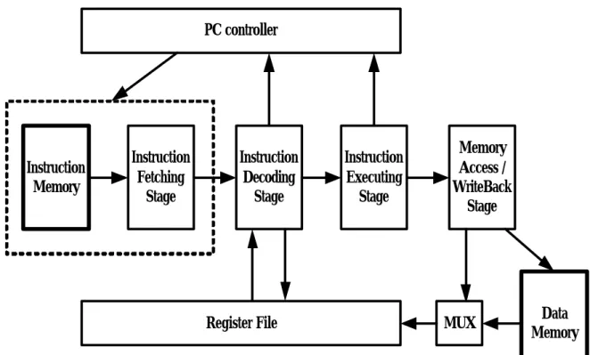
(7) In this paper, we illustrate the design of the AMIPS in section 2. We introduce the validation of AMIPS in section 3. And finally brief conclusions are discussed in section 4.. 2. Design of the Proposed AMIPS In this section, we will illustrate the detailed design and architecture of the AMIPS.. 2-1 Overview of the AMIPS The overall architecture of the AMIPS is shown in Figure 1. We use the instruction and memory files instead of thick frames (instruction and data memory). We don’t design cache for simplicity as well. The format of instruction file is one instruction per line and the content of the instruction is decimal representation. The format of memory file is one location per line and the content of the location is “mem_addr=mem_value”. So we combine instruction memory and instruction fetching stage to form our real IF stage. The dotted line represents the concept.. PC controller. Instruction Memory. Instruction Fetching Stage. Instruction Decoding Stage. Register File. Instruction Executing Stage. Memory Access / WriteBack Stage. MUX. Data Memory. Figure 1: The overall architecture of the AMIPS. 6.
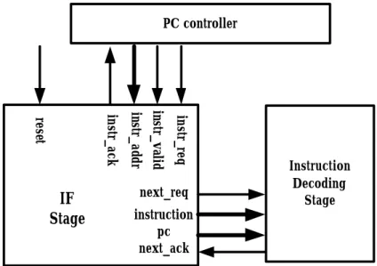
(8) 2-2 Design of the IF Stage The detailed interfaces of the IF stage are shown in Figure 2. It has the PC for fetching instruction from instruction file. The IF stage fetches instruction from instruction file by the value of PC in common, but when the instr_valid is ‘true’, the IF stage must change the value of PC to instr_addr and fetch the instruction from instruction file by the new value of PC. The situation occurs when the prior instruction is a branch or jump instruction which is taken. After the IF stage fetched the instruction, the IF stage sends the instruction and PC to the ID stage by using next_req, instruction, pc and next_ack ports. The reset port lets the IF stage return to the initial circumstance and it is low-enabled. PC controller. instr_req. instr_valid. instr_addr. instr_ack. reset. IF Stage. next_req. Instruction Decoding Stage. instruction pc next_ack. Figure 2: The interfaces of the IF stage and the interconnections between the IF stage, the PC controller and the ID stage.. 2-3 Design of the ID Stage The design of the ID stage is shown in Figure 3. The ID stage (decode module) is divided. into. three. sub-modules:. decode_latch,. decode_stage. and. 7.
(9) decode_complete. After fetching one instruction and sends the data to the ID stage, the decode_latch sub-module checks the value of last_req and start ports. If both of them are ‘true’, the decode_latch sub-module latches data, at the same time, it also sends data and control signal (end = ‘true’) to the decode_stage sub-module and also sends control signal (last_ack = ‘true’) to the IF stage. This indicates the data had latched and the IF stage can reset the communication protocol signals and the IF stage can start the next transaction. After the decode_latch sub-module sends the data and control signal (end) to decode_stage sub-module, the decode_stage sub-module performs the decoding action by using data from decode_latch sub-module and sends decoded results to the decode_complete sub-module. The decode_stage sub-module also sends the control signal (start = ‘false’) to the decode_latch sub-module. This indicates the ID stage is in working so that the decode_latch sub-module can’t latch data from the IF stage. The decode_stage sub-module also sends the control signal (no_zero = ‘true’) to decode_complete sub-module. The signal can combine the next_ack and other_ack signals to determine the control signal (self_reset = ‘true’ or self_reset = ‘false’) and sends decoded data to the EXE stage and the PC controller. We use the value (low-enabled) of self_reset to reset the decode_latch and decode_stage sub-modules. And then we get another instruction from the IF stage and next iteration starts.. 8.
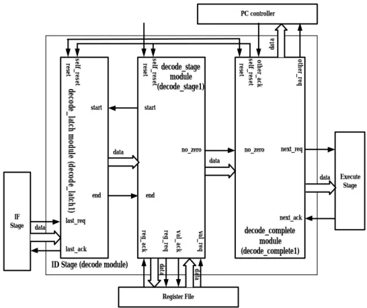
(10) data. PC controller. other_ack self_reset reset. other_req. start. no_zero. next_req. start. no_zero. data. data data end. next_ack. last_req val_req. val_ack. decode_complete module (decode_complete1). data. data. ID Stage (decode module). reg_req. last_ack. Execute Stage. end. reg_ack. data. self_reset reset. self_reset decode_latch module (decode_latch1) reset. IF Stage. decode_stage module (decode_stage1). Register File. Figure 3: The brief interfaces of the ID stage and the interconnections between the IF stage, the ID stage, the PC controller, the EXE stage and the register file.. After explaining the communications in the sub-modules, we show the detailed interfaces of the ID stage and interconnections of the IF stage, the ID stage, the PC controller, the register file and the EXE stage. It is shown in Figure 4. If it has to read the values of register, it uses the reg_* and val_* ports to get the values from register file. The branch port indicates the instruction whether it is a branch instruction. The jump port indicates the instruction whether it is a jump instruction. The pc_out port equals to the pc_in that is from the IF stage. The target port indicates the target address if the instruction is taken. The above ports are available when the instruction is a jump or branch instruction. The operation port tells the EXE stage to perform a kind of actions. The operand1 and operand2 are the operands of the action that the EXE stage performs. 9.
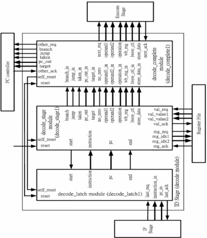
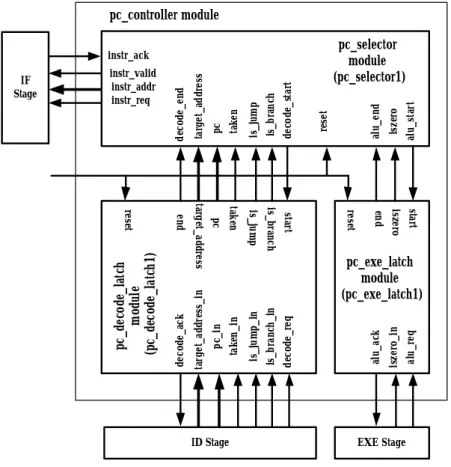
(11) The wb_reg port is the register specifier which writes back to register file. The lwsw_ctl port is the 5-bit control word for load and store instructions. The store_data port is only available when the instruction is a store instruction.. Figure 4: The interfaces of the ID stage and the interconnections between the IF stage, the ID stage, the PC controller, the EXE stage and the register file.. 2-4 Design of the PC controller The PC controller gets the necessary information from the ID stage and EXE stage and sends the correct value of PC to the IF stage. The PC controller is used to handle the branch and jump instructions. The detailed interfaces of the PC controller are shown in Figure 5. The PC controller (pc_controller module) has three sub-modules: pc_decode_latch, pc_exe_latch and pc_selector. The behavior of the pc_decode_latch and pc_exe_latch sub-modules is the same as. 10.
(12) the decode_latch sub-module introduced in section 2-3. After pc_decode_latch sub-module latches the information from the ID stage, the pc_selector sub-module gets the information (is_branch, is_jump, taken, pc and target_address) through port interfaces and sets the signal correct_address_ready to ‘true’. After pc_exe_latch sub-module latches the information from the EXE stage, the pc_selector sub-module gets the information (iszero) through port interfaces and now it has enough information (is_branch, is_jump, taken and iszero) to set the values of instr_valid and instr_addr ports. After sending the instr_valid and instr_addr to the IF stage, the pc_selector sub-module resets the signal correct_address_ready to ‘false’ for the next instruction. pc_controller module. iszero alu_start. reset. is_jump is_branch decode_start. alu_ack. iszero_in alu_req. pc_exe_latch module (pc_exe_latch1) is_jump_in is_branch_in decode_req. target_address. decode_end. pc taken pc_in taken_in. pc_decode_latch module (pc_decode_latch1). start iszero end. reset. is_jump. ID Stage. start is_branch. end. taken pc target_address. reset. decode_ack. instr_valid instr_addr instr_req. target_address_in. IF Stage. alu_end. pc_selector module (pc_selector1). instr_ack. EXE Stage. Figure 5: The interfaces of the PC controller and the interconnections between the IF stage, the ID stage, the PC controllers and the EXE stage.. 11.
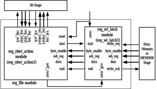
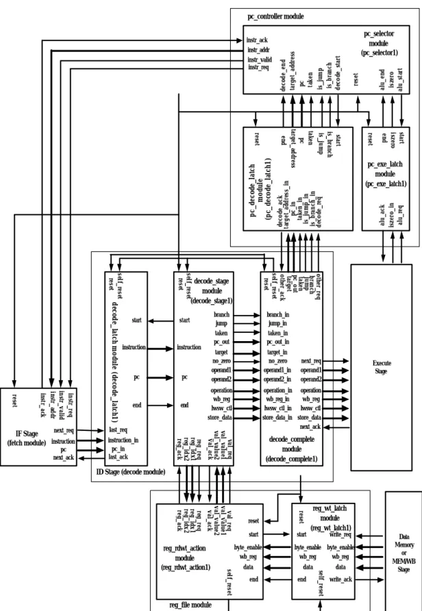
(13) 2-5 Design of the Register File The register file consists of 32 general-purpose 32-bit registers (r0 ~ r31) and two 32-bit registers (LO and HI) that hold the results of integer multiply and divide operations. The detailed interfaces of the register file are shown in Figure 6. The register file (reg_file module) has two sub-modules: reg_wt_latch and reg_rdwt_action. ID Stage. reset. val_req val_value1 val_value2 val_ack. reg_req reg_idx1 reg_idx2 reg_ack. start. start. byte_enable wb_reg data end. write_req. byte_enable byte_enable wb_reg wb_reg data data end. self_reset. self_reset. reg_rdwt_action module (reg_rdwt_action1). reset. reg_wt_latch module (reg_wt_latch1). Data Memory or MEM/WB Stage. write_ack. reg_file module. Figure 6: The interfaces of the register file and the interconnections between the ID stage, the PC controller and the data memory (or the MEM/WB stage).. After designing the IF stage, the ID stage, the PC controller and the register file, we must put it all together and it is shown in Figure 7.. 12.
(14) end. target no_zero operand1 operand2. target_in no_zero operand1_in operand2_in. operation wb_reg lwsw_ctl store_data val_req val_value1 val_value2 val_ack. reg_req reg_idx1 reg_idx2 reg_ack. val_req val_value1 val_value2 val_ack. last_req instruction_in pc_in last_ack. alu_end iszero alu_start. reset. alu_ack iszero_in alu_req. pc_decode_latch module (pc_decode_latch1) end. start iszero end. pc. reset. pc. start is_branch is_jump. branch_in jump_in taken_in pc_out_in. reg_req reg_idx1 reg_idx2 reg_ack. pc next_ack. instruction. pc_exe_latch module (pc_exe_latch1). other_req branch jump taken pc_out target other_ack self_reset reset. instr_req instr_valid instr_addr instr_ack. reset. next_req IF Stage (fetch module) instruction. branch jump taken pc_out. start. instruction. taken pc target_address end. reset. self_reset reset. self_reset decode_latch module (decode_latch1) reset. decode_stage module (decode_stage1). start. pc_selector module (pc_selector1). decode_ack target_address_in pc_in taken_in is_jump_in is_branch_in decode_req. instr_ack instr_addr instr_valid instr_req. decode_end target_address pc taken is_jump is_branch decode_start. pc_controller module. next_req operand1 operand2. Execute Stage. operation_in operation wb_reg_in wb_reg lwsw_ctl_in lwsw_ctl store_data_in store_data next_ack. decode_complete module (decode_complete1). ID Stage (decode module). end. start. reg_wt_latch module (reg_wt_latch1) write_req. byte_enable byte_enable wb_reg wb_reg data end. self_reset. data. reset. start byte_enable wb_reg. self_reset. reg_rdwt_action module (reg_rdwt_action1). reset. data. Data Memory or MEM/WB Stage. write_ack. reg_file module. Figure 7: The complete interconnections of the IF stage, the ID stage, the PC controller and the register file.. 13.
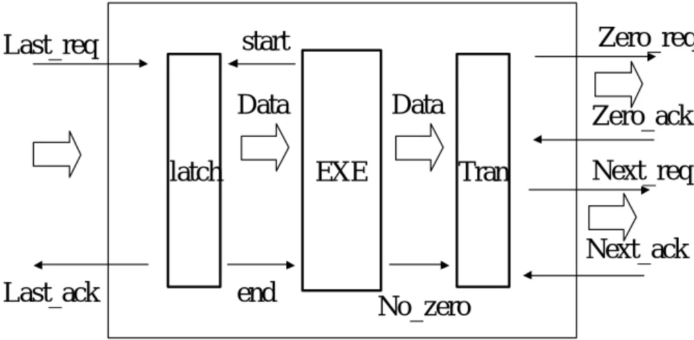
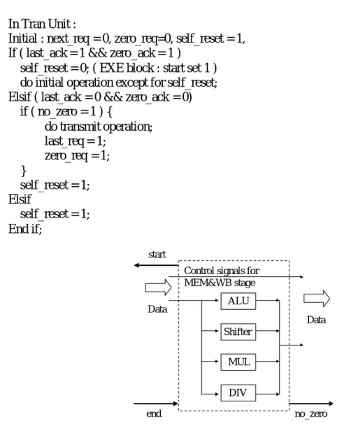
(15) 2-6 Design of the Execution Stage Zero_req. start. Last_req. Data latch. Data EXE. Zero_ack Tran. Next_req Next_ack. Last_ack. end. No_zero. Figure 8 The protocol in execution stage.. We can see the pseudo-code in the latch unit shown below : In Latch Unit : Initial : end = 0, last_ack = 0, When last_req=1 then if (start=1) … EXE Unit has finished previous operation { transmit the data to EXE Unit; last_ack = 1; end =1; } else don’t do any operation,wait for EXE Unit finish. When last_req = 0 then last_ack = 0 ;. The last two lines in the pseudo-code is used for four-phase data-bundled communication. The tran unit is used to communicate with next-stage and PC Controller and waits for the acknowledge signals (next_ack and zero_ack) from them. As soon as the tran unit receives the two control signals, it will send the self_reset control signal to reset the latch unit and exe unit. The pseudo-code in the tran unit is shown below :. 14.
(16) In Tran Unit : Initial : next_req = 0, zero_req=0, self_reset = 1, If ( last_ack = 1 && zero_ack = 1 ) self_reset = 0; ( EXE block : start set 1 ) do initial operation except for self_reset; Elsif ( last_ack = 0 && zero_ack = 0) if ( no_zero = 1 ) { do transmit operation; last_req = 1; zero_req = 1; } self_reset = 1; Elsif self_reset = 1; End if; start Control signals for MEM&WB stage Data. ALU Data Shifter MUL DIV. end. no_zero. Figure 9 The exe unit in AMIPS architecture.. The main function of the exe unit is to execute instructions. The details of the exe unit can be seen in Figure 9. The exe unit receives dual-rail data and the control signals from the latch unit. There are four kinds of functional units within the exe unit: integer ALU, integer multiplier, shifter and integer divider. We have one advantage in the AMIPS design. There is one bottleneck in most processor no matter it is synchronous processor or asynchronous processor. That is because it has slowest process in execution stage. But in the AMIPS design, it uses delay insensitive (DI) method to implement. So AMIPS has good performance.. 15.
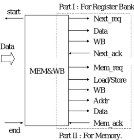
(17) 2-7 Design of the Memory Access and Writeback stage In this stage, our intention is to combine the Memory Access stage with Writeback stage together. Although the two stages are separated in synchronous processor which will load the data to Register Bank through Writeback stage, the design assumes that Memory will communicate with Register Bank directly. To prove this, we first examine the protocol of Memory Access and WriteBack stage (MEM&WB stage). Part I : For Register Bank.. start. Next_req Data WB. Data. Next_ack MEM&WB. Mem_req Load/Store WB Addr Data Mem_ack. end. Part II : For Memory.. Figure 10 The details of MEM&WB unit.. In Figure 10, two parts are included in the MEM&WB unit. Part I is register-type instructions which directly write the data calculated in the execution stage to Register Bank. Thus, only two signals, data and WB, are sent to Register Bank. Part II is memory-type instructions in which control signals, load and store, are used to communicate with memory. Besides, load and store include the “byte enable” information for memory, which is used for Register Bank. If the instruction to be processed is a load instruction, data of address in memory will be loaded to Register Bank. If it is a store instruction, the given data will be stored in memory. The detail architecture of MEM&WB stage is shown in Figure 11.. 16.
(18) Last_req. Execution stage. Latch Unit. MEM&WB Unit start. next_req. addr [32]. addr [32]. data [64]. data [64]. data [64]. wb [8]. Register Bank. next_ack Control [5] wb [8]. Control [5]. mem_req. wb [8]. Load/Store [5] wb [8]. Memory File. addr [32] Data [32]. Last_ack. mem_ack. end Self_reset. reset. Figure 11 The details architecture of MEM&WB stage.. 2-8 Design of the Memory File The MIPS R2000/3000 processors have a physical addressing range of 4 Gbytes (32 bits) and provide a full-featured memory management (MMU) unit that uses an on-chip Translation Lookaside Buffer (TLB). MMU can provide very fast virtual memory accesses. However, we don’t design the MMU in our AMIPS and instead, we use a “Memory File” to replace the MMU and virtual memory. However, the Register Bank receives only one request sent either from the MEM&WB stage or from the Memory File when an instruction is given at a time according to the MUX component in Figure 1. last_req. next_req. Load/Store [5] wb [8]. MEM&WB stage. addr [32]. Byte enable [4]. Memory File. wb [8] data [32]. Register Bank. Data [32]. last _ack. next_ack. Figure 12 The details architecture of memory file. 17.
(19) In real world, we don’t have the asynchronous memory but it doesn’t matter. Because of processor and memory have different clock domain in asynchronous design. So we use the asynchronous memory to replace the synchronous memory in our AMIPS design. After understanding the architecture of AMIPS processor, we can see the details of execution stage and MEM&WB stage in Figure 13.. 18.
(20) Figure 13 The details of Execution stage and MEM&WB stage. 19.
(21) 3. Validation of the AMIPS In this section, firstly, we validate the AMIPS at stage level, that is, check the correctness of each stage individually. Secondly, we validate the AMIPS at instruction level, that is, check the correctness of the instruction one by one. Finally, we validate the AMIPS at program level with some restrictions.. 3-1 Validation at Instruction Level The validation result at instruction level is summarized in Table 1. The number of special instructions is zero because we ignore the exception handling. All of the results of these checks and tests match the expected functionality. Name MIPS AMIPS MIPS AMIPS MIPS AMIPS. Instruction Format R-type instructions. I-type instructions. J-type instructions.. Number 28 26 28 28 2 2. Percentage (%) 92.85% 100% 100%. Table 1: Compare with MIPS and AMIPS. The table is categorized by instruction format.. 3-2 Validation at Program Level The format of our instruction file is one instruction per line ( in decimal machine code) and it is a pure text file. How do we get this kind of instruction file? The method that we use is shown in Figure 14. We use the complier, assembler and linker to generate the executable file and the S-record file. Then we use a program (rdsrec) of pmon toolset to generate the disassembled file. The goal of the rdsrec program is to read a Motorola S-record file and then it disassembles the file to standard output or a file. The disassembled file contains the format that we need. Finally, we use filter to generate the wanted. 20.
(22) instruction file. Finally, we can feed the AMIPS with instruction file. test program *.c. Instruction File instruction.txt pmon toolset (rdsrec). Filter. Complier. Assembler. Libraries. S-Record *.rec. Disassembled code *.txt. Linker. Executable File. AMIPS. Memory File memory.txt. Figure 14: The generation method of the instruction file.. We write a sort program to validate the correctness of the AMIPS. We put unsorted data in memory file and also write the sorted result to memory file. And then we can check the sorted result to validate the correctness of the AMIPS. We also count the number of instructions that AMIPS executed when we run the sort program by choosing different numbers of unsorted data, which are 20, 50 and 100. And the results accord with our expectation. It is summarized in Table 2. We also write two small programs: one is binary searching program and the other is Fibonacci program. We run the binary searching program by choosing different numbers of unsorted data, which are 20, 50 and 100. And the results accord with our expectation. It is summarized in Table 3. We run the Fibonacci program by choosing different numbers of unsorted data, which are 5, 20 and 40. And the results accord with our expectation. It is summarized in Table 4. Number of Unsorted Data 20 50 100. Instruction Count 4365 28867 116244. Sorted Result Correct Correct Correct. 21.
(23) Table 2: The number of unsorted data and its corresponding instruction count. (sort program). Number of sorted Data 5 20 100. Instruction Count 32 56 80. Searched Result Correct Correct Correct. Table 3: The number of sorted data and its corresponding instruction count. (binary searching program). Number of Fibonacci Series Instruction Count 5 47 20 167 40 327. Result Correct Correct Correct. Table 4: The number of Fibonacci series and its corresponding instruction count. (Fibonacci program). The above validation methodology is not good enough and it has some disadvantages. For example, the AMIPS cannot run big programs like benchmarks. It is because that the benchmarks always use the OS services (like File I/O). The solution of this problem is that the AMIPS should provide the interfaces for detection of the OS services. And the OS services can be done by C++ language. It is shown in Figure 15. We don’t implement the interfaces yet. However, after implementing the interfaces, the AMIPS will be more complete.. Instruction File instruction.txt. interface OS Services Output. interface. AMIPS. OS Services Input. Figure 15: The solution of the OS services problems.. 4. Conclusions In this paper, we design a proposed asynchronous processor AMIPS by using. 22.
(24) SystemC HDL. We validate the correctness of each component locally. We also validate the correctness of the AMIPS at the instruction level and program level. The AMIPS is the first prototype so we have some more things to do in the future. For example, we do not do the RTL synthesis yet since we do not have tools. Also, we have to design the asynchronous multiplier and divider. However, with this design, we can study some issues about the asynchronous architecture.. References [1]. SYSTEMC Version 2.0 Beta-2 User’s Guide, 1996.. [2]. Describing Synthesizable RTL in SystemC, Version 1.0, May 2001.. [3]. D. K. Arvind et al., “Micronets: A Model for Decentralising Control in Asynchronous Processor Architectures,” Asynchronous Design Methodologies, Proceedings, Second Working Conference, pp. 190-199, 1995.. [4]. A. Davis and Steven M. Nowick. An Introduction to Asynchronous Circuit Design. Technical Report UUCS-97-013, Department of Computer Science, University of Utah, Sep. 1997.. [5]. S.B. Furber, P. Day, J.D. Garside, N.C. Paver and J.V. Woods, “AMULET1: a micropipelined ARM,” Compcon Spring '94, Digest of Papers, pp. 476-485, 1994.. [6]. S.B. Furber, J.D. Garside, P. Riocreux, S. Temple, P. Day, Jianwei Liu and N.C. Paver, “AMULET2e: an asynchronous embedded controller,” Proceedings of the IEEE, Vol. 87, Issue 2, pp. 243-256, Feb. 1999.. [7]. S. Hauck. Asynchronous design methodologies: an overview. Proceedings of the IEEE, 83(1): 69-93, Jan. 1995.. [8]. G. Kane and J. Heinrich. MIPS RISC Architecture. Prentice Hall, 1992.. [9]. D.W. Lloyd and J.K. Garside, “A Practical Comparison of Asynchronous Design. 23.
(25) Styles,” Seventh International Symposium on, Asynchronous Circuits and Systems, pp. 36-45, 2001. [10] I.E. Sutherland, “Micropipelines,” Communications of the ACM, Vol.32, No.6, pp. 720-738, June 1989. [11] T. Werner and V. Akella, “Asynchronous processor survey,” IEEE Computer Vol 30, Issue 11, pp. 67-76, Nov. 1997. [12] J.V. Woods; P. Day, S.B. Furber, J.D. Garside, N.C. Paver, S. Temple, “AMULET1: an asynchronous ARM microprocessor,” Computers, IEEE Transactions on Computers, Vol. 46 Issue 4, pp. 385-398, Apr. 1997.. 24.
(26)
數據
+7
相關文件
Salas, Hille, Etgen Calculus: One and Several Variables Copyright 2007 © John Wiley & Sons, Inc.. All
了⼀一個方案,用以尋找滿足 Calabi 方程的空 間,這些空間現在通稱為 Calabi-Yau 空間。.
You are given the wavelength and total energy of a light pulse and asked to find the number of photons it
• ‘ content teachers need to support support the learning of those parts of language knowledge that students are missing and that may be preventing them mastering the
Wang, Solving pseudomonotone variational inequalities and pseudocon- vex optimization problems using the projection neural network, IEEE Transactions on Neural Networks 17
volume suppressed mass: (TeV) 2 /M P ∼ 10 −4 eV → mm range can be experimentally tested for any number of extra dimensions - Light U(1) gauge bosons: no derivative couplings. =>
Define instead the imaginary.. potential, magnetic field, lattice…) Dirac-BdG Hamiltonian:. with small, and matrix
incapable to extract any quantities from QCD, nor to tackle the most interesting physics, namely, the spontaneously chiral symmetry breaking and the color confinement..
