An Even Wiring Approach to the Ball Grid Array Package Routing
Shuenn-Shi Chen
1, Jong-Jang Chen
1, Chia-Chun Tsai
2, and Sao-Jie Chen
1 1Department of Electrical Engineering
National Taiwan University
Taipei, Taiwan, Republic of China
2
Department of Electronic Engineering
National Taipei University of Technology
Taipei, Taiwan, Republic of China
Abstract
An even-wiring router for the BGA package is presented in this paper to interconnect each I/O pad of a chip to a corresponding ball distributed on the substrate area. The major phases for the router consist of layer assignment, topological routing, and physical routing. Using this router, we can generate an even distribution of planar and any-angle wires to improve manufacturing yield. We have also conducted various testing examples to verify the efficiency of this router. Experiments show that the router produces very good results, far better than the manual design, thus it can be practically applied to VLSI packaging.
1. Introduction
In past years, package routing has been a missing link in the design process of integrated circuits because it was simple enough and could be done manually. Recently, the problem of package routing becomes more and more difficult when the I/O pin count gets larger and larger in array I/O packages, such as Pin-Grid-Array (PGA) and Ball-Grid-Array (BGA) packages. As a result, developing space-effective packaging tool for BGA packages becomes indispensable [1-5].
Recently, Yu and Dai [6] proposed an even fanout routing algorithm for a single-layer BGA package. They use a monotonic topological planar router for the fanout routing, where a pad and a ball of the same net have to be assigned to the same sector in a package. That is, the pad-to-ball nets are not allowed to cross one another and they should be symmetrical. As a result, all of the pad-to-ball nets can be easily routed on a single layer by the planar router. But in chip-set or processors design, the positions of solder balls are usually fixed such that the new design can reserve the same compatible function as a previous chip-set or processor. In this case, the planar routing on a single layer for each of pad-to-ball nets becomes more difficult [7] and even causes routing task failure.
To cope with the situation above, we propose in this paper a multi-ring based router for the BGA package. Then, we try to complete the pad-to-ball nets routing using less routing layers. Our proposed router is composed of layer assignment, topological routing, and physical routing phases, each of them will be depicted in this paper.
The reminder of this paper is organized as follows. Section 2 gives the problem formulation and routing model. Section 3 first presents an overview of the package router and then each phase of the routing algorithm will be detailed. The experimental results are reported in Section 4. Finally, Section 5 concludes this paper.
2. Problem Formulation
Assume that a BGA package contains a certain number of I/O pads arranged in a clockwise direction starting at an arbitrary side of the chip, and has the same number of solder balls distributed on the substrate area to form multiple rectangular rings on the substrate area as the ring routing space [8] as shown in Figure 1.
Based on the model of Figure 1, each ball location is fixed and no pin assignment [9] is allowed because a compatible chip (like the Intel mobile
Pentium II-series processors) must often have the
same solder ball positions as an off-the-shelf processor. The purpose of partitioning the routing area into such a multi-ring structure is to relax the sector restriction [6] and to handle the case of nets crisscross in the routing area.
I/O pad ball pitches ring 1 ring 2 ring r Inner-most ring Outer-most ring so ld er b a ll
3. Algorithm Description
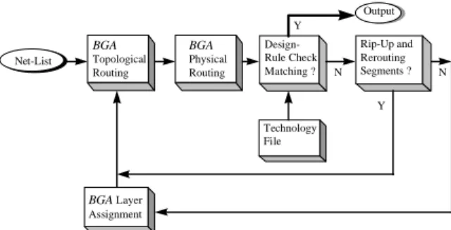
The general structure of our BGA package router is shown in Figure 2. The position descriptions of both pads and balls are served as the input of the routing system. From the input data, we cluster the balls ring by ring to form a multiple-ring structure.
BGA Layer Assignment Net-List Design-Rule Check Matching ? N Y Y BGA Physical Routing Rip-Up and Rerouting Segments ? Technology File Output BGA Topological Routing N
Figure 2. The structure of the BGA package router. The algorithm details related to the layer assignment, topological routing, and physical routing are depicted in the following subsections. The technology file contains mainly the upper-capacity limit of wires passing through the ball pitches. We apply a rip-up and rerouting step to change the routing direction of some segments to deal with design-rule violation. The above phases will be performed repeatedly until the routing of all nets has been done.
3.1 Layer Assignment
The layer assignment phase is employed to distribute nets to two or more distinct layers when some existing nets cannot be routed even after the rip-up and rerouting segment step. Some routing factors, like crossing number, detour lengths, and capacity in a ball pitch, will affect the routing result. Therefore, we must consider the above factors in assigning nets to layers. For above reason, let the weight of each net be W = k1V + k2D + k3C, where V,
D, and C represent the inversion value, inversion
distance, and inversion capacity respectively, and k1,
k2, and k3 are constants.
Using the notation of inversion-table [10] rather than graph based approach [11], we find two sets of
V, D, and C values as defined in the following. Here,
let (an, an-1, …, a1) be a permutation of sorted data (n,
n-1, …, 1), then (dn, dn-1, …, d1) represent the right
(left) inversion values V of (an, an-1, …, a1), where
every di represents the number of elements located at
the right (left) side of ai and greater (less) than ai. For
example, (2, 4, 5, 1, 3) is a permutation of sorted data {5, 4, 3, 2, 1}, then its R-Step and L-Step inversion values are (3, 1, 0, 1, 0) and (0, 1, 2, 0, 2), respectively. Again, assume ball i have an inversion
point ball j at a ring, where an inversion point of ball i in an R-Step (a L-Step) table is the first element
greater (less) than i scanning from right to left (from left to right). The inversion distance of ball i is defined as D = |m – n|, where m and n are the positions of ball i and its inversion point, ball j, respectively. On the other hand, the inversion capacity Ci of ball i is equal to measuring the number
of nets which may pass through between ball i and its inversion point, ball j. That is, the inversion capacity of ball i is calculated as Ci = |i - j| - 1. The above two
sets of V, D, and C values are stored in the R-Step and L-Step inversion tables, respectively.
Finally, we can assign nets having minimum weights in the L-Step inversion table to one layer and nets having minimum weights in the R-Step inversion table to another layer. For the example in Figure 3, nets (8, 5, 3, 7) have to be assigned to layer 1 and nets (4, 6, 2, 1) to layer 2, where k1, k2, and k3 are set to 1.
R-Step inversion table L-Step inversion table
4 6 2 8 1 5 3 7 4 6 2 8 1 5 3 7 Inv. value Inv. distance Inv. capacity Weight Inv. point 4 2 4 0 3 1 1 0 0 1 0 3 0 3 2 6 7 6 5 0 3 2 1 0 0 1 0 3 0 5 6 7 2 0 4 0 5 1 3 0 0 1 0 3 0 0 0 2 2 7 7 0 7 7 7 0 13 8 13 0 11 4 5 0 0 4 0 4 0 4 4 4 0 3 0 9 0 8 8 15 8 7 6 5 4 3 2 1 4 6 2 8 1 5 3 7 Layer 1 Layer 2 4 6 2 8 1 5 3 7 8 7 6 5 4 3 2 1 (b) Layer assignment (a) Inversion tables
Ball numbers
Figure 3. Illustration for the nets layer assignment.
3.2 Topological Routing
Since the topology paths of all the outer-ring balls have to pass through inner-rings toward pads, the routing of balls on an outer-ring should precede those on an inner-ring. The balls on the same ring are considered simultaneously and routed in a sequential net-ordering. Therefore, we treat all balls on a ring as a group, namely ring-group. Figure 4 shows that a ring-group is divided into two independent segments in which segment 1 and segment 2 have a rightward routing and a leftward routing, respectively. pad segment 1 segment 2 ball 3 2 4 1 5 6 10 9 8 7 ring group 5 4 3 2 1 10 9 8 7 6
(a) Partition two segments
5 4 3 2 1 10 9 8 7 6
(b) Rightward and leftward routing
3 2 4 1 5
segment 1 segment 2
6 10 9 8 7
Figure 4. Partition a ring-group into multiple segments.
To choose a better routing direction (toward left or right) for each segment in order to generate a shorter detour length is decided as follows: A leftward routing direction is made if the weight-sum of the inversion distances in the L-Step inversion table is smaller than the one in the R-Step inversion table and vice versa.
Afterwards, each of the independent segments will be transformed into a single row routing problem [12-13] with direction-constrained by shifting and rotating the corresponding row of pads to the left (or the right) side of the segments. Here, the term “direction-constrained” means that the wiring direction of a pad is upward only (whereas a ball can move upward or downward) for our BGA package routing. Figure 5 shows an example of the ball-side and pad-side interval diagram and how it corresponds to a direction-constrained single row routing. pad-side 7 3 1 5 1 3 5 segment 1 7 ball-side 1 2 3 4 5 6 7 reference line terminal insertion 2 6 4 segment 2 2 4 6 6 4 2 2 3 4 2
Figure 5. Transform segments into a direction-constrained single row routing. After having stretched out the reference line in Figure 5, which contains several extra nodes, we can obtain a planar topology layout by means of shifting and rotating pads back to their original positions, where the relative coordinates of balls and extra nodes are recorded from the right-side to the left-side of a ring-grid list (RGL). Therefore, an entirely planar layout for all nets in a multi-ring routing can be made.
3.3 Physical Routing
An entirely routing region can be partitioned into
r sub-regions by the ring-grid lists, where r is the
number of rings in a BGA package. For each sub-region, the vertical-grid lists (VGL’s) must be also constructed to form several independent bin-grids rather than using the rubber-band sketch [14]. Therefore, the routing problem in each bin-grid looks like a river routing [15] problem and can be solved by using a stack data structure. Whenever the path of any segment passes through a vertical-grid,
insert its net number (named as a redundant node) into the vertical-grid lists. Therefore, each net in the bin-grid can be routed by using a straight line to connect its two terminals. An example of any-angle wiring result can be generated as shown in Figure 6. Additionally, the rip-up and rerouting of a segment is performed only if we have to adhere to design rules or to reduce routing cost.
ring 1 ring 2 ring 3 12 11 10 9 8 7 6 5 4 3 2 1 14 13 16 15 17 18 20 19 21 3 5 8 17 10 22 23 16 15 13 12
bin-grid extra node
redundant node
Figure 6. An example of any-angle wiring result.
4. Experimental Results
The BGA package router was implemented on a
Pentium II-266 PC in Visual C++ language running
Windows-98. Since no this type of benchmarks are available from the literature, a set of twelve examples created by the authors are used to verify the efficiency of our BGA router. Tested results for the BGA router are reported in Table 1. The single-layer wiring result of a 200-ball BGA package (chip_12) is plotted in Figure 7, where some routing area is overcrowded because this chip essentially has serious crisscross among nets. Experimental results show that our router produces far better than the manual design in terms of routability and productivity.
5. Conclusions
An even routing tool for BGA packages is proposed in this paper. First, topological routing is used to generate a planar sketch and some of extra nodes on each ring-grid list. Then, physical routing is applied to complete an any-angle wiring layout for all the nets. In layer assignment, we calculate for each net a weight and then assign nets to suitable layers. To achieve a better codesign of both the proposed router and printed-circuit board (PCB) layout will be a challenging future work.
Acknowledgment
This work was supported by the National Science Council, Taipei, Taiwan, Republic of China, under Grant no. NSC 2215-E-002-037 and NSC 88-2216-E-027-003.
References
[1] J. H. Lau, Ball Grid Array Technology, McGraw-Hill, 1995.
[2] U. A. Shrivastsva and B. L. Bui, "Inductance calculation and optimal pin assignment for the design of pin-grid-array and chip carrier packages,"
IEEE Transactions on Components, Hybrids, Manufacturing Technology, vol. 13, pp. 147-153,
1990.
[3] C. C. Tsai, C. M. Wang, and S. J. Chen, "NEWS: A net-even-wiring system for the routing on a multilayer PGA package," IEEE Transactions on
Computer-Aided Design of Integrated Circuits and Systems, vol. 17, pp. 182-189, 1998.
[4] T. Hameenanttila, J. D. Carothers, and D. Li, "Fast coupled noise estimation for crosstalk advoidance in the MCG multichip module autorouter," IEEE
Transactions on Very Large Scale Integration (VLSI) Systems, vol. 4, pp. 356-366, 1996.
[5] D. Wang, P. Zhang, C. K. Cheng, and A. Sen, "A performance-driven I/O pin routing algorithm," in
Proc. IEEE Asia and South Pacific Design Automation Conference, (Hong Kong), pp. 129-132,
1999.
[6] M.-F. Yu and W. W.-M. Dai, "Single-layer fanout routing and routability analysis for ball grid array," in Proc. International Conference on
Computer-Aided Design, pp. 581-586, 1995.
[7] D. Richards, "Complexity of single-layer routing,"
IEEE Transactions on Computers, vol. C-33, pp.
286-288, 1984.
[8] D. C. Wang, "Pad placement and ring routing for custom chip layout," in Proc. 27th Design
Automation Conference, pp. 193-199, 1990. [9] M.-F. Yu, J. Darnauer, and W. W.-M. Dai,
"Interchangeable pin routing with application to package layout," in Proc. International Conference
on Computer-Aided Design, pp. 668-673, 1996. [10] D. E. Knuth, Sorting and Searching, vol. 3. Reading,
MA: Addison-Wesley, 1973.
[11] J. D. Cho, M. Sarrafzadeh, M. Sriram, and S. M. Kang, "High-performance MCM routing," IEEE
Design and Test of Computers, vol. 10, no. 3, pp.
27-37, 1993.
[12] E. S. Kuh, T. K. Kashiwabara, and T. Fujisawa, "On optimum single row routing," IEEE Transactions on
Circuits and Systems, vol. 26, pp. 361-368, 1979. [13] T. T.-K. Tarng, M. Marek-Sadowska, and E. S. Kuh,
"An efficient single row routing algorithm," IEEE
Transactions on Computer-Aided Design of Integrated Circuits and Systems, vol. CAD-3, pp.
178-183, 1984.
[14] W. W.-M. Dai, T. Dayan, and D. Staepelaere, "Topological routing in surf: generating a rubber-band sketch," in Proc. 28th Design Automation
Conference, pp. 39-44, 1991.
[15] C. P. Hsu, "General river routing algorithm," in Proc.
20th Design Automation Conference, pp. 578-583,
1983.
Figure 7. Single-layer wiring result of a 200-ball BGA package (chip_12).
Table 1. Routing results of different BGA package examples.
chip name # nets # rings # routing layers any-angle length (pixels) cpu-time (sec)
chip_1 72 3 1 7451 0.827 chip_2 72 3 1 8050 0.832 chip_3 72 3 2 7689 0.847 chip_4 72 3 1 10383 0.842 chip_5 112 4 1 10669 0.924 chip_6 112 4 1 10172 0.927 chip_7 112 4 1 11509 0.931 chip_8 144 4 1 15021 1.012 chip_9 144 4 1 17014 1.025 chip_10 144 4 1 15798 1.108 chip_11 200 5 1 21147 1.392 chip_12 200 5 1 21012 1.390