利用鎖相迴路改善主動鎖模雷射
58
0
0
全文
(2) 利用鎖相迴路改善主動鎖模雷射 Improving active harmonic mode-locked laser by PLL circuit 研 究 生 :王炫涵. Student : Xuan-an Wang. 指導教授 :陳智弘 老師. Advisor : Assistant Prof. Jyehong Chen. 國 立 交 通 大 學 光 電 工 程 研 究 所 碩 士 論 文. A Thesis Submitted to Institute of Electro-Optical Engineering College of Electrical Engineering and Computer Science National Chiao Tung University In Partial Fulfillment of the Requirements For the Degree of Master In Institute of Electro-Optical Engineering June 2005 Hsinchu, Taiwan, Republic of China. 中 華 民 國 九 十 四 年 六 月.
(3) ACKNOWLEDGEMENTS 很高興可以順利完成碩士班的學業,首先要感謝的人當然是亦師亦友的陳智 弘教授,他的確是位文武雙全且內外兼修不可多得的學者,他對待學生的好我想 當然是不在話下。當然還有嘉建學長幫我解惑一些難以啟齒的愚蠢問題,他將我 的無知赤裸裸看在眼底並不嫌棄我,並且因材施教有耐心的循循善誘。 另外在五樓的學長姐們更是我碩士生涯少不了要感謝的人,感謝他們商借儀 器,提供好的建議給我,甚至遇到問題也願意和我一起解決。我也祝福一起和我 畢業的夥伴們將來每個人都可以一帆風順,也期待明年學弟妹們和我們一樣快快 樂樂的度過這兩年,順利畢業。 千言萬語都無法詮釋這充滿回憶的實驗室,也希望未來能繼續發揚老師的實 驗室宗旨”健康第一”,大家都可以樂觀進取面對未來的所有挑戰。 最後感謝家人的包容,讓我無後顧之憂完成我的學生生涯。. 炫涵 2005/06/01. i.
(4) 利用鎖相迴路改善主動鎖模雷射 學生:王炫涵. 指導教授 : 陳智弘 老師. 國立交通大學光電工程研究所碩士班. 摘要 利用鎖模雷射做為光通訊的光源是現今的主流,要做為光通訊的光源要求脈 衝寬度窄且穩定的脈衝,本論文是利用鎖相迴路(PLL)的原理來應用達到這目 的。鎖相迴路中的 VCO 在我的架構中是用 PZT 取代,PZT 本身是壓電材料的光 纖,PZT 的長度改變可以經由信號產生器的信號和光纖環腔中的信號通過 mixer 再利用低通濾波器取出接近直流值的電壓來送進 PZT,控制 PZT 長度,藉此來 做回授的機制。 本實驗發現沒有 PLL 電路下的主動鎖模雷射,操作在 10G 情形下穩定時間 為 10 分鐘,timing jitter 為 1 ps。但如果加上 PLL 的機制可以穩定達到 40 分鐘, 並且可以改善 timing jitter 為 500fs。. ii.
(5) Improving active harmonic mode-locked laser by PLL circuit Student:Xuan-Han Wang. Advisor : Dr. Jyehong Chen. Institute of Electro-Optical Engineering National Chiao Tung University. Abstract In recent years , the current optical communication source is mode-locked laser. The optical communication source require the pulse width short and the pulse stable. In this thesis , I utilize the PLL circuit to achieve it . In my experiment setup , the PZT is instead of the VCO in the PLL , the PZT is a piezoelectric material fiber . The PZT length can be changed by letting signals producing from the synthesizer and the signal in the ring cavity pass through the mixer , and then the signals pass through the low pass filter to control the PZT . It is my feedback . If I operate at 10G without PLL in my experiment , the pulse will only maintain about 10 minutes and then distortion . If I utilize the PLL circuit , the pulse can maintain for forty minutes and improve the timing jitter to 500fs .. iii.
(6) CONTENTS Acknowledgements............................................................................................ i Chinese Abstract................................................................................................. ii English Abstract.................................................................................................. iii Contents................................................................................................................. iv List of Figures...................................................................................................... vi List of Tables........................................................................................................ vii. CHAPTER 1 1.1. Introduction. The history of the fiber lasers........................................................... 1. 1.2.1 Review of PLL…………………....................................................................... 4 1.2.2 Linear Phase Locked Loop………………………………………………………5 1.2.3 Digital Phase Locked Loop.................................................................................. 6 1.2.4 All Digital Phase Locked Loop………………………………….........................7 1.3. The motivation of research………………………………………………………9. 1.4. The organization of these thesis…..……………………………………………10. CHAPTER 2. Basic Concepts. 2.1 Theory of the active mode locked laser……….............................................11 2.1.1 Amplitude modulation mode locked...................................................................11 2.1.2 Phase modulation mode locked.................................................................... …..13 2.1.3 Harmonic mode-locked....................................................................................15 2.2 Theory of the PLL circuit...................................................................................... 17 2.2.1 PLL basics…...……………………………………............................................17 2.2.2 General PLL block diagram………................................................................. 19 2.2.3 Unique features of the PLLs as control loops………………………………….20 2.3. Math for PLL…………………………………………………………………...21 iv.
(7) 2.3.1 Typical simplifying steps……………………………………………………….21 2.3.2 Standard nonlinear model for analog PLL……………………………..………22 2.3.3Standard linear model for analog PLL………………………………………….23. CHAPTER 3. Experimental setup and results. 3.1 Introduction of my experiment setup………………........................... 24 3.1.2 Double balance mixer………...………….......................................................... 25 3.1.3 Low pass filter…..….……………………………............................................. 26 3.1.4 PZT………………...…………………….......................................................... 30 3.2.1 Introduction of the experimental setup............................................................... 33 3.2.2 Operating at 10 GHz without PLL..................................................................... 35 3.2.3 Feedback circuit……………………………………………………................. 38 3.3.1 Operating at 10 GHz with PLL …………......................................................... 39 3.3.2 Optical time division multiplexing..................................................................... 41. CHAPTER 4. Conclusions and improvement. 4.1. Conclusions…………………………………………………………………….43. 4.2. Improvement…………………………………………………………………...43. Reference.................................................................................................................45. v.
(8) LIST OF FIGURES Fig.1.1. APLL block diagram. Fig.1.2. DPLL block diagram. Fig.1.3. ADPLL block diagram. Fig.2.1. Amplitude modulation in the time domain. Fig. 2.2. Principle of actively mode-locking explained in the frequency domain. Fig. 2.3. Time domain of phase modulation. Fig. 2.4 Fig. 2.5 Fig. 2.6. Development of pulse train in time domain by superposition of modes Phase lock loop basic component Phase lock loop block diagram. Fig. 2.7. Phase lock loop math type. Fig. 2.8. Phase lock loop nonlinear model. Fig. 2.9. Phase lock loop linear model. Fig. 3.1. structure of the double balance mixer. Fig. 3.2. A passive low-pass filter showing impedance values. Fig. 3.3. An active low-pass filter. Fig. 3.4. Low pass filter frequency response. Fig. 3.4. SOA curves. Fig. 3.5 PZT operate at 1G Hz with different input voltage Fig. 3.6 Mode-locked Erbium-doped fiber ring laser and stabilization scheme(Dashed line), where “PC” is polarization controller and “SIF” is step index fiber Fig. 3.7 Basic experimental setup Fig. 3.8. The waveform operated at 10GHz is measured by Agilent 86116A. Fig. 3.9. The waveform operated at 10GHz is measured by Agilent 86116A. (a) (b) (c)it shows the changing of the pulse as time pass by.. Fig. 3.10 Optical spectrum Fig 3.11 The waveform measured by autocorrelator Fig. 3.12. RF spectrum vi.
(9) Fig. 3.13 Feedback circuit Fig. 3.14 Experiment setup with feedback loop Fig. 3.15 The waveform operated at 10GHz is measured by Agilent 86116A Fig. 3.16. Bit Rate multiplier block diagram. Fig. 3.17. 20 GHz Waveform by Bit Rate multiplier. LIST OF TABLES Table 1-1. Phase-Locked Loop Comparison. Table 3.1 result of the double balance mixer Table 3.2 variation of voltage by changed the delay line. vii.
(10) CHAPTER 1 INTRODUCTION 1.1 The history of fiber lasers In early 1930 , there have been some scientists purposed to use fiber as a medium of transmission waveguide of the light. However , in that age , manufacture of purification of glass and technology of semiconductor was not developed as well as what we see today. Besides ,there was no reliable light source, and the insertion loss of fiber was very large. The loss of transmission was above 1000dB per kilometer before. Therefore it didn’t not adapt to fiber optical communication system. Until 1960, Mainman , an American scientist, demonstrated a ruby laser and the first laser was born in the world. In 1962, Hall and Nathan etc. , they invented a GaAs semiconductor laser. It improved the idea of transmission of using fiber as a medium of the waveguide. In 1966, Gao-kun, non-Chinese citizen of Chinese origin, propose this idea. The great contributions of these people open the door of the fiber optical communication system.. A fiber amplifier can converted into a laser by placing it inside a cavity designed to provide optical feedback. Such lasers are called fiber lasers. Many kinds of rare-earth ions, such as erbium(Er), neodymidum(Nd), and ytterbium(Yb), can be used to make fiber lasers capable of operating over a wide range of wavelength extending from 0.4 to 4μm. The first fiber laser , demonstrate in 1961, was based on an Nd-doped fiber with 300μm core diameter , but it had high insertion loss. In 1973, low-loss silica fibers were used to build diode-pumped fiber lasers and soon after such fibers become available. 1.
(11) However , it was not until the late 1980s that fibers began to attract a lot of interests in research. The initial emphases of the research were on Nd- and Er-doped fiber lasers.Nd-doped fiber lasers are of considerable practical interest since they can be pumped by GaAs semiconductor lasers operating near 0.8μm . On the other hand , Er-doped fiber lasers can operate in several wavelength regions , ranging from visible to far infrared . The wavelength of 1.55μm regions has attracted the most attention because it coincides with the low-loss region of silica fibers for optical communication application.. The performance of Erbium-doped fiber lasers (EDFLs) improves considerably while they are pumped at 980 or 1480 nm wavelength, because of the absence of the excited-state absorption. The 980nm pump wavelength yields higher gains than a 1480 nm pump at high powers. This comes from the fact that 980 nm has achieved a higher inversion than 1480nm. But the amplified spontaneous emission (ASE) starts growing as the pump power is increased ; the higher inversion created at the beginning of the fiber by the 980nm pump creates a better seed for the forward ASE than that created by the 1480nm pump. In public , there are three kinds of pomping. Furthermore the wavelength of pumping power and pumping mechanisms are decided by the applications and demands of the EDFLs.. As early as 1989 , a 980nm-pumped EDFL exhibited a slope efficiency of 58% against the absorbed pump power. They also exhibited good performances when pumped at 1480nm. The choices between the pumping wavelength 980 and 1480nm and structures are not always clear since each pumping way has its own merits.. 2.
(12) In a 1989 experiment on active mode-locking, 4ps pulses were generated by using a ring cavity which included 2km of standard fibers with large anomalous GVD. In 1992, a fiber laser provided 3.5 to 10ps pulse with a transform-limited time-bandwidth product of 0.32 at the repetition rate up to 20GHz. The laser was used in a system experiment to demonstrate such a laser source which can be use in soliton communication systems at the bit rate up to 8Gb/s. In the same year, a stabilization scheme for a mode-locked erbium fiber laser which relies on locking the pulse phase with that of the drive source was reported. In 1993, a EDFL produced 6ps pulse at the repetition rate up to 40GHz and with the output wavelength tunable over a wide range of 40 to 50nm. In 1999 , the technique of regenerated mode locking with phase locked loop(PLL) produce a 40GHz pulse train with tuning range from 1530 to 1560 and pulsewidth as short as 0.9ps by using a soliton effect in the fiber cavity. It was also demonstrated for ultrahigh-speed optical communication in the time(TDM) and frequency domains(WDM). Using the dispersion-managed soliton technique and soliton effect, the 1 Tb/s WDM soliton transmission and ultrahigh speed optical TDM transmission which exceeds 1Tb/s was achieved.. Passive mode locking is an all-optical nonlinear technique capable of producing ultra-short optical pulse, without requiring any active component, such as a modulator, inside the laser cavity. Saturated absorbers have been used for passive mode locking since early 1970s. It is sole method available for use until the invention of the additive-pulse mode locking techniques emerged. Additive-pulse mode-locked was first demonstrated in a soliton laser by Mollenauer and Stolen(1984). Subsequent research showed that this method can be applied to non-soliton systems as well. In 1992, the technique of non-linear polarization rotation was first used in order to build passive mode-locked fiber lasers and it was quickly demonstrated that stable and 3.
(13) self-starting pulse trains of subpicosecond pulse at a 42MHz repetition rate can be generated by using this technique. Moreover, ultra-short pulses less than 100fs at a repetition rate of 48MHz were obtained in a ring cavity configuration in which the net dispersion was positive.. As short as femto-second pulses and stable ultrahigh-speed pulse train can be available respective from the passive mode-locked fiber laser and the active mode-locked fiber laser. With these advantages and different characteristic, nowadays, fiber lasers have been widely used in several different areas especially for the ultrahigh-speed fiber optical communication and nonlinear optics experiments.. 1.2.1Review of PLL The phase-locked loop (PLL) helps keep parts of our world orderly. If we turn on a television set, a PLL will keep heads at the top of the screen and feet at the bottom. In color television, another PLL makes sure that green remains green and red remains red. A PLL is a circuit, which causes a particular system to track with another one. More precisely, a PLL is a circuit synchronizing an output signal (generated by an oscillator) with a reference or input signal in frequency as well as in phase. In the synchronized —often called locked — state, the phase error between the oscillator’s output signal and the reference signal is zero, or very small. If phase error builds up, a control mechanism acts on the oscillator in such a way that the phase error is again reduced to a minimum. In such a control system the phase of the output signal is actually locked to the phase of the reference signal. This is why it is referred to as a phase-locked loop (PLL). The very first PLL were implemented as early as 1932 by de Bellescize; this French engineer is considered inventor of the “coherent communication.” The PLL found broader industrial applications only when it becomes available as an integrated 4.
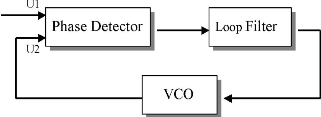
(14) circuit (IC).. The first PLL ICs appeared around 1965 and were purely analog. devices. An analog multiplier (four-quadrant multiplier) was used as the phase detector, the loop filter built from a passive or active RC filter, and the well-known voltage-controlled oscillator (VCO) was used to generate the output signal of the PLL. This type of PLL is referred to as the “linear PLL” (LPLL) today. In the following years the PLL drifted slowly but steadily into digital territory. The very first digital PLL (DPLL), which appeared around 1970, was in effect a hybrid device; only the phase detector was built from a digital circuit, e.g., from an EXOR gate or JK-flipflop, but the remaining blocks were still analog. A few years later, the “all-digital” PLL (ADPLL) was invented. The ADPLL is exclusively built from digital function blocks, hence doesn’t contain any passive components like resistors and capacitors. analogy to filters, PLLs can also be implemented “by software.”. In. In this case, the. function of the PLL is no longer performed by a piece of specialized hardware, but rather by a computer program. This last type of PLL is referred to as SPLL.. 1.2.2 Linear Phase Locked Loop The LPLL ( also known as Analog Phase-Lock Loop (APLL) ) is a traditional PLL as shown in Figure 1.1, which was proposed back in 1930s.. Phase Detector (PD) can. detect the different phase error between the reference clock and the output clock. PD can be a four phase analog multiplixer or analog signal mixer. Loop Filter (LP) is a filter to filter high frequency signal and noises from PD and environment. The output of Loop Filter is a DC value to send to Voltage Control Oscillator ( VCO) to generate desired frequency. Through the closed feedback loop, the PLL can lock the input reference clock phase and frequency.. 5.
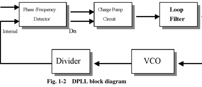
(15) 1.2.3 Digital Phase Lock Loop Figure 1.2 shows the DPLL. The components of DPLL are : Digital Phase Frequency Detector (PFD), Analog Charge Pump, Analog Loop Filter, Analog Voltage Control Oscillator, and Frequency Divider (FD). Phase Frequency Detector can detect the phase and frequency error between Frequency Divider output and input reference clock. The outputs of PFD are Up or Down signals to Charge Pump to charge capacitor. Loop Filter is a kind of low pass filter filtering noise and high frequency signal and send out the DC value to Voltage Control Oscillator. The Phase Frequency Detector can detect rising edge or falling edge to check the phase error. The output of Phase Frequency Detector can be the value of phase error or high/low (Up/Down) signal to Charge Pump. Phase Frequency Detector can be the basic logic gate (XOR, NAND, OR…,etc.). The input signal of Phase Frequency Detector is square wave but not the sine wave.. Frequency Divider circuit make output clock. reach a N times rate to reference clock with the same phase. The DPLL is a hybrid system which contains analog and digital design techniques. Designer should have more skills with mixed-signal designs.. 6.
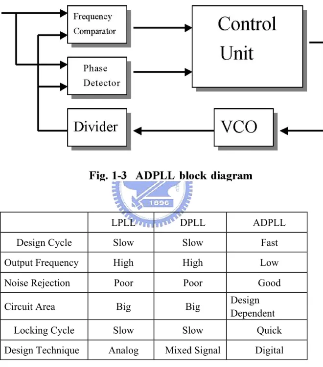
(16) Fig. 1-2 DPLL block diagram. 1.2.4 All Digital Phase Lock Loop All Digital Phase-Locked Loop (ADPLL) consists full digital component: Digital Phase Frequency Detector, Digital Control Unit, Digital Control Oscillator, and Digital Frequency Divider as shown in figure 1-3.. An ADPLL does not have any. passive component such as capacitor and resistor.. All signals in the ADPLL are. digital signals. The analog VCO was replaced by the digital VCO. The Phase Frequency Detector detects the frequency difference and the phase difference between the reference clock and the feedback signal.. The Control Unit receives the signals to. control the DCO. By including a divide-by –N divider in the feedback path, the DCO clocks runs N times faster than input reference clock. The functional blocks of the ADPLL imitate the functions of the corresponding analog blocks. Because the ADPLL consists of dgital circuits entirely, they are many different of design methods to achieve the functions of them. The ADPLL system is a discrete-time system, hence analyzing the ADPLL in S-domain is not suitable.. The ADPLL system can be. analyzed in time-dimain or Z-domain, or building a new model to analyze the ADPLL 7.
(17) system. Because of no analog components, the ADPLL is a very high noise rejection PLL design. The whole system can be designed by basic logic gates.. LPLL. DPLL. ADPLL. Design Cycle. Slow. Slow. Fast. Output Frequency. High. High. Low. Noise Rejection. Poor. Poor. Good. Circuit Area. Big. Big. Locking Cycle. Slow. Slow. Quick. Design Technique. Analog. Mixed Signal. Digital. Design Dependent. Table 1-1 Phase-Locked Loop Comparison. 8.
(18) 1.3 The motivation of research Fiber optical transmission using a short optical pulse strain is a fundamental technology in order to achieve a high-speed and long distance global network. For ultra-high speed fiber optical communication, the characteristic of ideal transmission source is demanded to be stable, widely tunable wavelength, transform limited, low timing jitter, adjustable pulsewidth, and high extinction ratio. Therefore a mode-locked erbium-doped fiber lasers source with high repetition rate and short pulsewidth is good selection for ultra-high speed communication system. Besides, these ML-EDFLs can produce higher output power and lower insertion loss in all fiber system. In order to achieve the ML-EDFLs stable for a long time, improving it by PLL circuit is a good method. A Phase-Locked Loop circuit is a modern interesting electronic building block widely applied in electronics and wireless communication systems.. As mentioned above, there are several types to realize phase shifter. function. Among the versatile investigations, continuously tuning the phase of microwave signal or optical clock via optical or optoelectronic technique has been extensively studied since its particular applications in phased-array antennas (PAAs), wireless or fiber communications and the electro-optic sampling (EOS) system. In electronics, a phase-locked loop (PLL) is a closed-loop feedback control system that maintains a generated signal in a fixed phase relationship to a reference signal. Since an integrated circuit can hold a complete phase-locked loop building block, the technique is widely used in modern electronic devices, with signal frequencies from a fraction of a cycle per second up to many gigahertz. So in my thesis, I will describe how the PLL application in the ML-EDFLs.. 9.
(19) 1.4 The organization of this thesis This thesis is consisted four chapters. Chapter 1 introduce the history of laser, PLL and my motivation. In Chapter 2, it will describe the principle of mode locked laser and PLL. In chapter 3, I will present my experiment result and analysis it. Finally, chapter 4 will give conclusions and improvement.. 10.
(20) CHAPTER 2 BASIC CONCEPTS 2.1 Theory of the active mode locked laser 2.1.1 Amplitude modulation mode locked Amplitude modulation mode-locking is a method to produce a short pulse train and high repetition rate by directly modulating the optical amplitude of the light. It can be analyzed both in the time and frequency domains. In the time domain, the amplitude modulation provides a time dependent loss so that only the pulses which pass through the modulator at the lowest loss will exist. As the pulses pass through the modulator continually, the pulsewidth will get shorter and shorter. However, shorter pulses will experience larger dispersion and finally the two forces balance each other to form the steady state pulse shape. In this way, the modulation time period must be equal to a multiple of the roundtrip time for producing stable pulses. Figure 2.1 shows the active mode-locking process in the time domain.. Fig. 2.1 Amplitude modulation in the time domain 11.
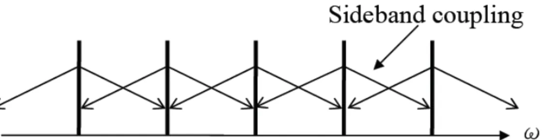
(21) In frequency domain, we can assume that the center frequency of signal gain profile is νo, and the amplitude of the central mode without amplitude modulation is expressed as ε(t) = E0 cos(ωot). The transform function of the active amplitude modulator, which controls the loss of light in the cavity, can be written as. and fm is modulation frequency, such as the signal after modulation can be expressed as following. where ∆m is modulation index. It is clear from this equation that the center frequency νo induces two side modes with fixed phase relationship νo ± fm while it experiences modulation of active modulator. Similarly, after these two side modes which are made by center frequency νo go through the active amplitude modulator, there will also increase other new side modes νo± 2 fm with fixed phase relationship. These sidebands can injection-lock the neighboring modes sequentially and finally the mode-locking is achieved. (See figure 2.2). The modes that are separated every. fm will be phase-locked, and short pulses. can be formed in the time domain. When N equals to 1, the laser is mode locked at the fundamental repetition rate. When N is an integer greater than 1, the laser is harmonic mode locked.. 12.
(22) Fig. 2.2 Principle of actively mode-locking explained in the frequency domain. 2.1.2. Phase modulation mode locked. Phase modulation mode-locking is a method to produce a short pulse train by modulating the optical phase. It can also be analyzed both in the time and the frequency domains. In the time domain, the phase modulator provides a periodic phase change for the optical pulse. If the pulsewidth is much smaller than the modulation period, the change of the optical phase produced by the phase modulator can be expressed as:. where φ o is a constant phase, and the influence of φ o on optical pulse can be dφ. neglected . The first order term dt. will influence the central frequency of the pulses dφ. and shifting magnitude of influence depends on its value. Therefore, if dt t ≠ 0, the central frequency of optical pulse will be changed. In another word, the pulse will dφ. experience smaller gain and center frequency will still be changed, if dt t is still not equal to zero. This is unstable and will not lase. Only the pulses which pass through 13.
(23) dφ. the PM modulator and experience maximum gain is at dt t = 0 , and its every round trip is able to be stable. Then, it will lase. ( See fig. 2.3). Fig. 2.3 Time domain of phase modulation d 2φ. As regarding the second order term dt 2. t 2 ≡ ηt 2 , it adds a chirp to the pulse.. Also, it will affect the optical bandwidth of the pulses. The effect can be expressed in mathematics by:. ∆ω = where. ∆ω. 1. τ2. + ητ 2. is the bandwidth of optical pulse, τ is the pulsewidth , and. η=. d 2φ dt 2. is. the chirp parameter. In the frequency domain, we can assume that the central frequency is νo . When it passes through the phase modulator, the electric field of the pulse can be written as:. 14.
(24) where fm is the modulating frequency of phase modulator, ∆m is the modulation index, and Jn is the n-th order Bessel function. If νo is one of the harmonic modes in the laser cavity and fm is N times magnitude of the fundamental harmonic frequency of the cavity, these harmonic modes (νo +k fm ) will have the fixed phase relation with the νo , where K=±1, ±2, ±3, , ,etc la. Therefore, all these harmonic modes will have fixed phase relation. In time domain, these harmonic modes will create constructive interference at periodic time and destructive interference at other times by injection-locking.(see fig. 2.4). Fig. 2.4 Development of pulse train in time domain by superposition of modes. 2.1.3 Harmonic mode-locked A continuous wave erbium ring laser can be actively mode-locked by using an amplitude or phase modulator to generate pulses at the modulation frequency. 15. fm.
(25) where fc is the cavity mode-spacing frequency, c is the speed of light, L is the cavity length and n is the refractive index of the cavity. These pulses have a round trip time of tr , which is related to fc and the pulse width τ as following,. This is known as fundamental mode-locking, and it produces pulses at repetition rate equal to fm .The cavity mode-spacing frequency of a typical laser cavity is of the order of 0.5~6MHz. To increase the pulse repetition rate, pulses could be produced at integer harmonics of the cavity mode-spacing by modulating at a frequency fm , given by. where P is an integer representing the number of longitudinal modes locked, and ranges from a few hundred to tens of thousand. This is known as harmonic mode locking, these longitudinal modes with equal interval Pfp is called as supermodes, and its new round trip time shows as following,. In 1970s, the KS theory predicted that with amplitude mode-locking the time bandwidth product is 0.441 for a chirp-free Gaussian pulse and 0.315 for a Sech2 pulse. Furthermore, it states that the pulsewidthτis inversely proportional to (δ ) ( f m • ∆f 3dB ). τ= K٠ (. 1. 4. , so that. 1 f m •∆f 3 dB. 1. ) 2 (δ ). 1. 4. (a) 16. 1. 4. and.
(26) where δ is the effective single-pass amplitude modulation depth, ∆f 3dB is the 3dB gain band width of the laser cavity and K is a pulse shape-dependent constant. It is clear from this equation that with increasing modulation frequency and increasing modulation amplitude, the optical pulsewidth will be narrowed. However, though we can use this way to promote higher repetition rates, the drawback of harmonic mode-locking is not stable for a long time. We will discuss it later. Actually, the smallest pulsewidth and chirp of the pulses can be estimated by using the time-bandwidth product of transform limited. For chirp free Gaussian sharp, time bandwidth product is 0.441. For Sech2 sharp, time bandwidth product is 0.315. We can use this transform-limited to appraise our laser. However, the exact estimate is not possible since the cavity dispersion is not considered in equation (a).. 2.2 Theory of the PLL circuit 2.2.1 PLL basics Phase locked loop has three basic components ; a phase detector ,a loop filter , a voltage-controlled oscillator. The phase detector is a device that produces a measure of the difference in phase between an incoming signal and the local replica .As the incoming signal and the local replica change with respect to each other, then the phase difference becomes a time-varying signal into the loop filter. The loop filter governs the PLL's response to these variation in the error signal . The VOC device that produces the carrier replica . The voltage control oscillator , as the name implies ,is a sinusoidal oscillator whose freq. is controlled by a voltage level at the device input.. 17.
(27) Fig. 2.5 Phase lock loop basic component ‧ Basic idea of a phase-locked loop: – inject sinusoidal signal into the reference input – the internal oscillator locks to the reference – frequency and phase differences between the reference and internal sinusoid ⇒ k or 0 – Internal sinusoid then represents a filtered version of the reference sinusoid. – For digital signals, Walsh functions replace sinusoids.. 18.
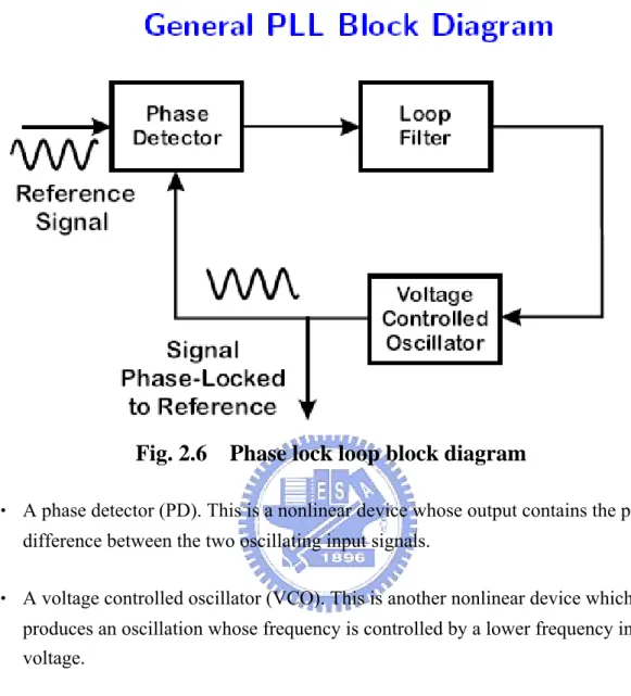
(28) 2.2.2General PLL block diagram. Fig. 2.6 Phase lock loop block diagram ‧ A phase detector (PD). This is a nonlinear device whose output contains the phase difference between the two oscillating input signals.. ‧ A voltage controlled oscillator (VCO). This is another nonlinear device which produces an oscillation whose frequency is controlled by a lower frequency input voltage.. ‧ A loop filter (LF). While this can be omitted, resulting in what is known as a first order PLL, it is always conceptually there since PLLs depend on some sort of low pass filtering in order to function properly.. ‧ A feedback interconnection. Namely the phase detector takes as its input the reference signal and the output of the VCO. The output of the phase detector, the phase error, is used as the control voltage for the VCO. The phase error may or may not be filtered.. 19.
(29) 2.2.3Unique features of the PLLs as control loops ‧ Correct operation depends on being nonlinear. Phase detector action (frequency to phase) and VCO action (phase to frequency) are nonlinear. Different parts of loop are in different spaces (signal response and phase response).. ‧ PLLs are almost always low order (not counting various high frequency filters and parasitic poles). Typically first or second order. A few third or fourth order loops.. ‧ With the exception of PLL controlled motors, the PLL designer is responsible for designing/specifying all the components of the feedback loop. Complete feedback loop design replaces control law design, and the designer’s job is governed only by the required characteristics of the input reference signal, the required output signal,and technology limitations of the circuits themselves.. ‧ PLL control of motors, the motor and optical coupler takes the place of the VCO. The rest is at the designer's discretion.. ‧ Control theory used in most PLL texts is straight linear system design with a small amount of nonlinear heuristics thrown in.. ‧ Stability analysis and design of the loops is combination of linear analysis, rule of thumb, and simulation.. ‧ Experts in PLLs tend to be electrical engineers with hardware design backgrounds. ‧ General theory of PLLs and ideas on how to make them even more useful seems to cross into the controls literature only rarely.. 20.
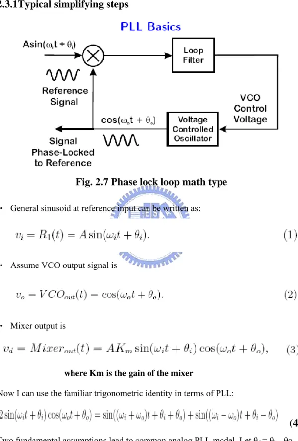
(30) 2.3. Math for PLL. 2.3.1Typical simplifying steps. Fig. 2.7 Phase lock loop math type ‧ General sinusoid at reference input can be written as:. ‧ Assume VCO output signal is. ‧ Mixer output is. where Km is the gain of the mixer Now I can use the familiar trigonometric identity in terms of PLL:. (4) Two fundamental assumptions lead to common analog PLL model. Let θd = θi – θo. Then the assumptions are : 1 ) The first term in (4) is attenuated by the high frequency low pass filter in and by 21.
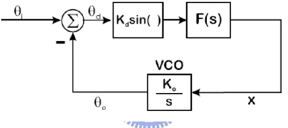
(31) the low pass nature of the PLL itself. 2 ) Let ωi ≈ ωo, so that the difference can be incorporated into θd. This means that the VCO can be modeled as an integrator. 3 ) The baseband phase detector output is then:. 2.3.2Standard nonlinear model for analog PLL. Fig. 2.8 Phase lock loop nonlinear model As show as fig. 2.4, it still a nonlinear system. The typical analysis methods include: 1) Linearization: For θd small sin θd ≈ θd and cos θd ≈ 1. Useful for studying loops that are near lock, does not help when θd is large. 2) Phase plane portraits. Classical graphical method of analyzing behavior of low order nonlinear systems about a singular point. Can only completely describe first and second order systems. 3) Simulation. Explicit simulation of the entire PLL is relatively rare. Problem is stiff. Simulations that sample fast enough to characterize the 2ωot term are often far too slow to effectively characterize the baseband.. ⇒ Simulate the response of the components (phase detector, filter, VCO) in signal 22.
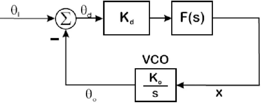
(32) response space.. ⇒ Simulate the entire loop only in signal phase space.. 2.3.3Standard linear model for analog PLLs. Fig. 2.9 Phase lock loop linear model Used for most analysis and measurements of PLLs. Model has some omissions: 1) The texts typically omit the input bandpass filter.. ‧ Not in the loop itself & the actual input frequency is often not known or is variable. ‧ The designer has some idea of the range of the signal. ‧ Input bandpass filter can considerably reduce broadband noise entering the system.. 2) The texts typically omit the high frequency low pass filter. The loop filter is optimized for the stability and performance of the baseband (phase).. 3) Amplitude of the phase error is dependent upon A( Mixer output ), the input signal amplitude. The linearized model has a loop gain that is dependent upon the loop components. Thus, in practical loop design, the input amplitude must either be regulated or its affects on the loop must be anticipated.. 23.
(33) CHAPTER 3 EXPERIMENTAL SETUP AND RESULTS. 3.1 Introduction of my experiment setup My experiment utilizes the active mode locked fiber laser to generate short pulsewidth, high output power, and repetition rate 10G pulsetrain. To make pulsetrain steady, I use the phase locked loop application in my experiment. As my thesis describe previously , PLL has three basics;phase detector , low pass filter , and voltage control oscillator . In my experiment, the phase detector is a double balance mixer, the low pass filter is a RC circuit, and the voltage control oscillator is the PZT. The double balance mixer has two inputs and one output. In these two inputs, one is the signal of the ring and another is the synthesizer signal, and then this output delivers into the low pass filter. When it passes through the low pass filter, only the frequency difference between incoming and local signal can pass. Finally the difference of the frequency term will control the PZT to match the length at the right time. Because the PZT is a fiber which can change its length by input voltage, this three basics will describe clearly in latter section.. 24.
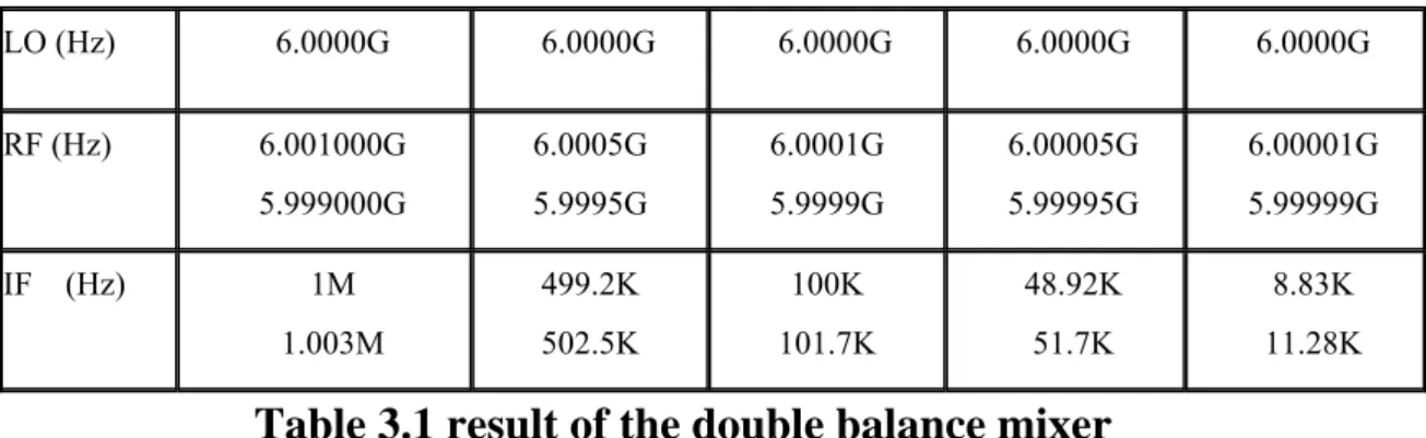
(34) 3.1.2 Double balance mixer Introduction The double balance mixer is not only a phase detector but also a frequency detector. However, in my experiment, the double balance mixer is just for a phase detector. The double balance mixer has two inputs and one output. (See fig.3.1) These two inputs one is LO port and another is RF port. The output is the IF port. We assume LO port signal is A1sin(ω1 t+Φ1) and RF port signal is A2sin(ω2. t+Φ2). The output IF port signal is 1/2A1 A2sin[(ω1 t –ω2t) +(Φ1–Φ2)] and 1/2A1 A2sin[(ω1 t +ω2t) +(Φ1+Φ2)]. So the double balance mixer is also a multiplier.. IF. LO. Double. RF. balance mixer. Fig. 3.1 structure of the double balance mixer Operation The double balance mixer is a passive device, so the operation is easily. What we need to pay attention to is take care of the RF and LO port, which available frequency range is 6~18G Hz. The frequency range of the IF port is DC~3000M Hz. Also the LO port input power operates about 10dBm.. Performance As what I described previously, the double balance is a frequency detector. I use 6G Hz signal to test it. Table 3.1 is the result.. 25.
(35) LO (Hz). 6.0000G. 6.0000G. 6.0000G. 6.0000G. 6.0000G. RF (Hz). 6.001000G. 6.0005G. 6.0001G. 6.00005G. 6.00001G. 5.999000G. 5.9995G. 5.9999G. 5.99995G. 5.99999G. 1M. 499.2K. 100K. 48.92K. 8.83K. 1.003M. 502.5K. 101.7K. 51.7K. 11.28K. IF. (Hz). Table 3.1 result of the double balance mixer By the same token, the double balance mixer is the phase detector. I used the synthesizer to connect the RF and LO port, but the LO port was added a delay line. Then I measure the IF port variation when I change the delay time. When I change the phase from 0 to 2πby the delay line. We can find that the IF output with variation of phase induced variation of voltage. (See Table 3.2). LO. RF. IF (Vpp). 0 dBm. -5dBm. 1000 mv. -6dBm. -5dBm. 600 mv. -10dBm. -5dBm. 340 mv. 0 dBm. -11dBm. 500 mv. 0 dBm. -15dBm. 310 mv. 0 dBm. -25dBm. 100 mv. Table 3.2 variation of voltage by changed the delay line. 3.1.3 Low pass filter Introduction A low-pass filter passes low frequencies fairly well, but attenuates, or blocks, 'high' frequencies. (The low frequencies are relative to the unwanted higher frequencies and therefore do not have a definitive range. The actual frequencies that. 26.
(36) are cut vary from filter to filter.) Therefore it is also called a high-cut filter or treble cut filter. A high-pass filter is the opposite, and a bandpass filter is a combination of a high- and low-pass. The concept of a low-pass filter exists in many different forms, including electronic circuits (like a hiss filter used in audio), digital algorithms for smoothing sets of data, acoustic barriers, blurring of images, and so on. Low-pass filters play the same role in signal processing that moving averages do in some other fields, such as finance; both tools provide a smoother form of a signal which removes the short-term oscillations, leaving only the long-term trend.. Passive electronic realization. Fig. 3.2 A passive low-pass filter showing impedance values One simple electrical circuit that will serve as a low-pass filter consists of a resistor in series with a load, and a capacitor in parallel with the load. The capacitor exhibits reactance, and blocks low-frequency signals, causing them to go through the load instead. At higher frequencies the reactance drops, and the capacitor effectively functions as a short circuit. The break frequency, also called the turnover frequency or cutoff frequency (in hertz), is determined by the choice of resistance and capacitance:. 27.
(37) or equivalently (in radians per second):. One way to understand this circuit is to focus on the time the capacitor takes to charge. It takes time to charge or discharge the capacitor through that resistor. At low frequencies, there is plenty of time for the capacitor to charge up to practically the same voltage as the input voltage. At high frequencies, the capacitor only has time to charge up a small amount before the input switches direction. The output goes up and down only a small fraction of the amount the input goes up and down. At double the frequency, there's only time for it to charge up half the amount. Another way to understand this circuit is with the idea of reactance at a particular frequency. Since DC cannot flow through the capacitor, DC input must "flow out" the path marked Vout (analogous to removing the capacitor). Since AC flows very well through the capacitor — almost as well as it flows through solid wire — AC input "flows out" through the capacitor, effectively short circuiting to ground (analogous to replacing the capacitor with just a wire). It should be noted that the capacitor is not an "on/off" object (like the block or pass fluidic explanation above). The capacitor will variably act between these two extremes. It is the bode plot and frequency response that show this variability.. 28.
(38) Active electronic realization. Fig. 3.3An active low-pass filter Another type of electrical circuit is an active low-pass filter. In this example, the cutoff frequency (in hertz) is defined as:. or equivalently (in radians per second):. The gain in the passband is -R1/ R1, and the stopband drops off at −6 dB per octave, as it is a first-order filter. Many times, a simple gain or attenuation amplifier (See operational amplifier) is turned into a lowpass filter by adding the capacitor C. This decreases the frequency response at high frequencies and helps to avoid oscillation in the amplifier. For example, an audio amplifier can be made into a lowpass filter with cutoff frequency 100 kHz to reduce gain at frequencies which would otherwise oscillate. Since the audio band (what we can hear) only goes up to 20 kHz or so, the frequencies of interest fall entirely in the passband, and the amplifier behaves the same way as far as audio is concerned.. 29.
(39) Performance LPF 6 5. Gain. 4 3 2 1 0 1. 10. 100. 1000. Frequency(Hz). Fig. 3.4 Low pass filter frequency response My low pass filter was designed the same as Fig 3.3. Fig. 3.4 is the low pass filter frequency response; from it we can find the 3dB cut-off frequency is 100Hz.. 3.1.4 PZT Introduction The PZT , PFM-50C-NCTU , Piezoelectric Fiber Modulator System is a bench top instrument designed for research applications. This instrument uses a piezoelectric ceramic actuator that rapidly and precisely “stretches” optical fiber coils and creates many millimeters of path length change in response to a analog input command. The. PFM-50C-NCTU. System. includes. PFM-Actuator.. 30. the. PFM-Board-BT. and. the.
(40) The PFM-Board-BT, Bench Top Electronic Power and Control Board, is an integrated 1200-volt power supply and amplifier that is optimized to drive and control the piezoelectric actuator. These electronics are installed in a chassis with cooling fan to insure safety, cool operation and minimum electrical noise. The fan opening should always be kept clear so that airflow is not restricted. A plug-in-the-wall transformer is provided to supply DC power to the chassis. The PFM-Actuator, Piezoelectric Actuator/Fiber Coil Assembly is a self contained module that is electrically connected to the PFM-Board-BT and has two optical fibers ready for splicing into the customers optical experiment.. The PFM-50C-NCTU is designed for easy user installation and operation:. ‧ Only standard AC line power is required. ‧ The customer’s analog control signal connects directly to the SMA connector on the chassis. This signal is amplified to drive the piezoelectric actuator.. ‧ The customer’s optical fiber is easily spliced to the bare fiber leads provided in the PFM-Actuator module.. Operation The input is driven by a 0-10 volt signal that may or may not contain a bias component. Typical scanning is performed with a sine or ramp waveform of up to 100Hz. If a ramp is used, the fall time should not be excessively short. Software should prevent the end user from selecting scan rates and amplitudes that exceed the SOA (Safe Operating Area) see fig. 3.4. Operation outside the SOA may result in will activate protective circuitry to limit current consumption. Continued operation in this mode will result in increased power dissipation and heat generation. The red LED will 31.
(41) indicate operation outside the SOA and may be accompanied by clicking and buzzing of the PFM-Board.. Fig. 3.4 SOA curves Performance I utilize the PZT in my experiment to optimize the cavity length . The PZT DC input is 0~10 V, and it’s length can be stretch 0~4.5mm . The length change with the input voltage is direct proportion . So when I mode locked my fiber laser with the PZT , at the same time, if I change the PZT input bias , the mode locked pulse shape will be distortive , because the fit frequency drift . If I want to mode locked it again , I must be change the modulate frequency from the synthesizer . So the mode locked frequency range is also direct proportion with the PZT input voltage. See fig. 3.5. For example , if I operate at 1 G Hz , the tunable frequency range is 70k~80k . 32.
(42) 80 kHz. Fig. 3.5 PZT operate at 1G Hz with different input voltage. 3.2.1 Introduction of the experimental setup In 1992, for active mode-locked fiber laser, the stabilization mechanism used relied on locking the electrical phase of output optical pulse to that of the drive source have been demonstrated. To stabilize the laser, they developed the phase-locking circuit shown within the dashed line. (See Fig.3.6) A length of erbium-doped fiber wound on a piezoelectric crystal (PZT). It works as voltage control oscillator (VCO). A fraction of the laser output is detected by a photodiode, amplified and filtered with a narrow bandwidth filter to generate a sinusoidal signal. The frequency mixer work as a phase detector which compares the phase of the pulse train and that of the drive source (synthesizer). The error signals will occur from the mixer while there are influences affecting the fiber cavity with time. Simultaneously, the displacement of 33.
(43) the PZT which was controlled by error signals feedback adjusts the length of the fiber cavity to compensate the perturbation of the fiber cavity caused by mechanical vibrations or temperature variations.. In this paper, once the output pulse is locked in this way, it is possible to tune the synthesizer by ±5~6 KHz with a very little change in either pulsewidth or bandwidth. Actually, this tuning range corresponds to the change of the fiber length wound on PZT, which is also limited by the amplifier output voltage range. Besides, the speed of the phase-locking circuit is limited by the response of the high voltage amplifier. As a result, only thermal drifts and vibrations of a few hundreds of Hertz can be effectively suppressed. However, it is enough to overcome the influence of generally environmental perturbation to the fiber laser.. Fig. 3.6 Mode-locked Erbium-doped fiber ring laser and stabilization scheme(Dashed line), where “PC” is polarization controller and “SIF” is step index fiber. 34.
(44) 3.2.2 Operating at 10 GHz without PLL 980 nm LD All PM-fiber in the cavity WDM coupler. PM-EDF. PM isolator 40Gb/s EOspace intensity modulator. coupler. AM 10% coupler AMP 50%. output. 50%. synthesizer. Fig. 3.7 Basic experimental setup Our basic experiment setup is shown in fig. 3.7. This fiber laser consisted of a polarization-maintaining erbium-doped fiber (PM-EDF), a WDM coupler, a 10/90 coupler, a polarization-maintaining (PM) isolator, and a LiNbO3 intensity modulator. There are all polarization maintaining fibers in the cavity and the total length of the laser cavity is about 50m. Therefore we can calculate the fundamental frequency to be 4MHz.. Fig. 3.8 is measured by Agilent 86116A. By using the Agilent precision time base 86107A, the timing jitter is smaller than one picoseconds. The measuring pulsewidth of the laser is about 13ps and the optical spectral bandwidth is about 0.375nm shown in fig. 3.10. Fig.3.11 shows the waveform measured by autocorrelator.. At the beginning, we have optical pulse shown in fig. 3.9(a), but it only can stabilize for a few minutes. Fig. 3.8 shows the changing of the pulse in time domain, and finally, it become unlocked. Therefore, the pulse would broaden and the timing jitter would be getting larger as time pass by.. 35.
(45) Fig. 3.8 The waveform operated at 10GHz is measured by Agilent 86116A.. (a). (b). Fig. 3.9 The waveform operated at 10GHz is measured by Agilent 86116A. (a) (b) (c)it shows the changing of the pulse as time pass by.. 36.
(46) Fig. 3.10 Optical spectrum autocorrelator at 10GHz Gaussion fitting. 70 60 50 ) . u. a( y ti s n et ni. 40 30 20 10 0 0. 5. 10. 15. 20 Time (ps). 25. 30. 35. 40. Fig 3.11 The waveform measured by autocorrelator Fig. 3.11 shows the pulse-width measured by autocorrelator. The solid line is Gaussian fitting curve and pulse-width is measured about 11ps. The RF spectrum is shown in fig. 3.12 and the span of the spectrum is 50MHz. The supermode suppression ration (SMSR) is about 45dB. 37.
(47) Fig. 3.12 RF spectrum. 3.2.3 Feedback circuit Utilizes these devices and combines it to demonstrate the feedback circuit(see Fig. 3.13). The feedback loop has five components: double balance mixer, low pass filter, weighted summer, high voltage controller, and PZT. The weighted summer has tow input. One is LPF output, another is DC Bias. The DC Bias in order to make the PZT stretch a length which can change the cavity short or long. PZT. ω1 ω2 MIXER. LPF. Summer. Bias. Fig. 3.13 Feedback circuit. 38. HVC.
(48) 3.3.1 Operating at 10 GHz with PLL 980 nm LD WDM PM EDF Optical path Electrical path. PZT. AM. PM isolator. O/E. Delay line. DBM. LPF. Input. Weighted. Input. summer. DC Bias 5V. Fig. 3.14 Experiment setup with feedback loop Using additional feedback circuit, as shown in Fig.3.14, we can have better experiment results. Because of the environmental reason, the length of the fiber cavity has random variations, and it would cause the pulse detected by the O/E converter (11982A) have a time shift. The signal generated by synthesizer and O/E converter is connected in LO and RF port of double balanced mixer (DBM). We can get the amplitude A(t )[1 + cos(2ωt )] in IF port, and cos(2ωt ) can be ignored by using low pass filter (LPF). Therefore, the final value A(t ) means the amplitude generate from the output port of ring. The differential amplitude is caused by timing phase difference and that is affected by the length difference of the cavity. The cavity length is changed by mechanical vibrations or temperature variations. We can change the fundamental. 39.
(49) frequency by changing a length of erbium-doped fiber on a piezoelectric crystal (PZT). Comparing with section 3.2.2, we can make the system more stable with PLL feedback loop. Fig. 3.15 shows the result of the steady pulse in 40 minutes. In this experimental setup, the system can steady for more than one hour. The pulsewidth of the laser measured by autocorrelator is always steadily within 11ps. The RF spectrum is shown in figure 4.8 and the span of the spectrum is 50MHz. The supermode suppression ration (SMSR) is about 48dB.. 40.
(50) Fig.3.15 The waveform operated at 10GHz is measured by Agilent 86116A. 3.3.2. Optical time division multiplexing. 41.
(51) Fig. 3.16 Bit Rate multiplier block diagram I use the Bit Rate multiplier (BRM) for an OTDM application. (see Fig. 3.16) The BRM multiplies input pulse train repetition rates by 2, 4, 8, and 16. This is accomplished by dividing the input pulse into separate legs of a Mach-Zehnder fiber interferometer. One leg provides a variable pulse delay and amplitude equalization, while the other leg produces a fixed bit-pattern delay. The two pulses are then recombined to produce a repetition rate of two times the input rate. The BRM-T-4 unit has two cascaded stages and has an optical output from the first stage so that the user can access a 2× pulse train for initial application setup. The BRM-T-8 unit implements the same principle as the BRM-T-4, possessing three cascaded stages, while the BRM-T-16 unit has four cascaded stages. They have an optical output from. 42.
(52) the previous stage to allow the user to access 8× and 16× pulse trains for initial application setup.. Fig. 3.17 20 GHz Waveform by Bit Rate multiplier I input the 10GHz pulse train into the BRM, we can find the 20GHz waveform (see Fig. 3.17). The timing jitter is 1 ps.. CHAPTER 4 CONCLUSIONS AND IMPROVEMENT 43.
(53) 4.1 Conclusions A stable optical short pulse source operated at the gigahertz region is strongly required for realizing future ultrahigh-speed optical communication. Many characteristics of mode-locked fiber lasers are much better than semiconductor lasers, such as good pulse quality, transform-limited, and high output power, especially for operating at ultrahigh repetition rate. Besides, among many mode-locking techniques for pulse lasers, active mode-locking is a simple and reliable method for generating stable pulse train in gigahertz regions. Undoubtedly, for application of communication, the active mode-locked erbium-doped fiber laser (AML-EDFL) is a good choice. In this study, in order to reduce the timing jitter, and maintain the pulse train . I utilize the PLL circuit to achieve it. From the experimental results we find that timing jitter reduce 50% with the PLL circuit. The pulse train maintains 40minutes.. 4.2 Improvement There are some other methods to improve this AML-EDFL. First, the center wavelength of the AML-EDFL can become tunable by placing a wider bandwidth of optical tunable filter in the cavity. Second, a generation of femtosecond pulses in the gigahertz region becomes more and more important in terms of realizing terabit/second communication. As the simulation results, the drawback of active mode-locking, wider pulsewidth can be overcome by placing a length of dispersion shift fiber (DSF) in the cavity. With dispersion management, the balance of self phase modulation (SPM) and group velocity dispersion (GVD) can shorten the wider pulsewidth of active mode-locked fiber laser. Third, the polarization beam splitter (PBS) can be put into laser cavity since it can ensure that the state of the polarization in the cavity aligns to the slow axis of PM fiber. In this way, it is able to build a the powerful active mode-locked erbium-doped fiber laser (AML-EDFL) with stable (low 44.
(54) amplitude jitter), high repetition rate, widely tunable wavelength, transform limited, low timing jitter, short pulsewidth, and high extinction ratio pulse train for application of ultra-high speed fiber optical communication.. References [1] E. Snitzer, “Optical maser action of Nd in a barium crown glass”, Physical review letters, 7, 1961, pp.444 45.
(55) [2] J. Stone and C. A. Burrus, Appl. Phys. Lett. 23, 388 (1973).. [3] P. C. Becker, N. A. Olsson, J. R. Simpson, “Erbium-Doped Fiber Amplifiers-Fundamentals and Technology”, ACADEMIC PRESS, 1997, pp. 162-163. [4] W. L. Barnes, S.B. Poole, J. E. Townsend, L. Reekie, D. J. Taylor, and D. N. Payne, “Er-Yb and Er doped fiber lasers”, J. Lightwave Technol. 1989, 7, pp. 1461. [5] J. D. Kafka, T. Baer, and D. W. Hall, “Mode-locked erbium-doped fiber laser with soliton pulse shaping”, Opt. Lett., 1989, 14, pp. 1269 [6] H. Takara, S. Kawanishi, M. Saruwatari, and K. Noguchi, “Generation of highly stable 20 GHz transform-limited optical pulses from actively mode-locked Er3+-doped fibre lasers with an all-polarisation maintaining ring cavity”, Electron. Lett., 1992, 28, pp. 2095. [7] X. Shan, D. Cleland, and A. Ellis, “Stabilising Er fiber soliton laser with pulse phase locking”, Electron. Lerr., 1992, pp.182. [8] T. Peiffer and G.. Veith, “ 20 GHz pulse generation using a widely tunableall-polarisation preserving erbium fibre ring laser”, Electron. Lett. , 1993, pp.1849. [9] Eiji Yoshida, Naofumi Shimizu, and Masataka Nakazawa, “A 40-GHz 0.9-ps regeneratively mode-locked fiber laser with a tuning range of 1530-1560 nm”, IEEE Photonics Technology Letters, 1999, 11, pp. 1587. 46.
(56) [10] M. Nakazawa, “ Solitons for breaking barriers to terabit/second WDM and OTDM transmission in the next millennium”, IEEE J. on selected topics in Quant. Electron., 2000 , pp. 1332. [11] L. F. Mollenauer and R. H. Stolen, “ The soliton laser”, Opt. Lett., 1984, pp.13. [12] K. J. Blow and D. P. Nelson, “ Improved mode locking of an F-center laser with nonlinear nonsoliton external cavity”, Opt. Lett., 1988, pp.1026. [13] V. J. Matsas, T. P. Newson, D. J. Richardson, and D. N. Payne, “Selfstarting passively mode-locked fibre ring soliton laser exploiting nonlinear polarization rotation”, Electron. Lett., 1992, pp.1391. [14] K. Tamura, H. A. Haus, and E. P. Ippen, “ Self-starting additive pulse mode-locked erbium fibre ring laser”, Electron. Lett., 1992, pp.2226. [15] K. Tamura, L. E. Nelson, H. A Haus, and E. P. Ippen, “ Soliton versus nonsoliton operation of fiber ring lasers”, Appl. Phys. Lett., 1994, pp. 149. [16] P. P Vasil’ev., V. N Morozov., G. T. Pak, Y. U. Popov, M. Yu, and A. B. Sergeev, “Measurement of the frequency shift of a picosecond pulse from a mode-locked injection laser” Sov. J. Quant. Electron., 1985, PP.859. [17] C. J. Chen, P. K. A. Wai, and C. R. Menyuk, Opt. Lett., 1994, pp.198. [18] C. S. Tsai, “Study of an active harmonic mode-locked fiber laser stabilized by a semiconductor optical amplitude”, Institute of Electro-Optical engineering in NCTU, master thesis, 2003 47.
(57) [19] Govind P. Agrawal, “Applications of Nonlinear Fiber Optics”, Academic Press, Chap. 5, 2001. [20] R.L. Fork, B. I. Greene, and C.V. Shank, “Generation of optical pulse short than 0.1 psec by colliding pulse mode locking”, Appl. Phys. Lett.,1981, pp. 671. [21] H. A. Haus, J. G. Fujimoto, and E. P. Eppen, “Structure for additive pulse mode locking”, J. Opt. Soc. Am. B., 1991, pp. 2068. [22] K. Tamura, E. P. Ippen, H. A. Haus, and L. E. Nelson, “77-fs pulse generation form a stretched-pulse mode-locked all-fiber ring laser”, Opt. Lett., 1993, pp.1080. [23] S. Y. Chen and J. Wang, “Self-starting issues of passive self-focusing mode locking”, Opt. Lett., 1991, pp.1689. [24] Herman A. Haus, “Mode-locking of Lasers”, IEEE J.on Selected topics in Quant. Electron., 2000, pp. 1173. [25] M. P. Tian, “High repetition rate femtosecond hybrid mode-locked Er-fiber lasers by asynchronous modulation”, Institute of Electro-Optical engineering in NCTU, master thesis, 2003. [26] D. J. Kuizenga, and A. E. Siegman,”FM and AM mode locking of the homogeneous laser-PartΙ:Theory ”, IEEE K. Quant. Electron., 1970, QE-6,(11), pp.694-708. 48.
(58) [27] S.G. Edirishinghe, and A.S. Siddiqui, “Stabilised 10GHz rationally mode-locked erbium fibre laser and its use in a 40Gbit/s RZ data transmission system over 240km of standard fibre” IEE Proc.-Optoelectron., 2000, pp. 401-406. [28] Z. Ahmed, and N. Onodera, “High repetition rate optical pulse generation by frequency multiplication in actively mode-locked fibre ring lasers”, Electron. Lett., 1996, pp. 55-57. [29] R. Kiyan, O. Deparis, O. Pottiez, P. Megret, and M. Blondel, “Long term stable operation of a rational harmonic actively mode locked Er doped fiber laser with repetition rate doubling” Proc. of European Conf. on Optical Communication, ECOC’93, September 1999, Nice, France, pp. 180-181. [30] M. Nakazawa, E. Yoshida and Y. Kimura, “Ultrastable harmonically and regeneratively modelocked polarization-maintaining erbium fiber ring laser”, Electron. Lett., 1994, pp. 1603. [31] Ivan P. Kaminow and Tingye Li, “Optical fiber telecommunications IVB –System and Impairments” ACADEMIC PRESS, 2002, Ch 12 [ 32] VPIphotonics, “Photonic Modules Reference Manual”, 2003. [33] Jinno, M., “Effects of crosstalk and timing jitter on all-optical time-division multiplexing using a nonlinear fiber Sagnac interferometer switch”, IEEE J. Quantum Electron. Lett., 1994, pp. 2842. 49.
(59)
數據
+7
相關文件
The differential mode of association: Understanding of traditional Chinese social structure and the behaviors of the Chinese people. Introduction to Leadership: Concepts
• A sequence of numbers between 1 and d results in a walk on the graph if given the starting node.. – E.g., (1, 3, 2, 2, 1, 3) from
It is based on the probabilistic distribution of di!erences in pixel values between two successive frames and combines the following factors: (1) a small amplitude
Regardless of terminal or network logins, the file descriptors 0, 1, 2 of a login shell is connected to a terminal device or a pseudo- terminal device. Login does
除了新聞報導,可以查看網路 評價(如 Google
Windows 95 後的「命令提示字 元」就是執行 MS-DOS 指令的應用
定期更新作業系統 定期更新作業系統,修 正系統漏洞,避免受到
17-1 Diffraction and the Wave Theory of Light 17-2 Diffraction by a single slit.. 17-3 Diffraction by a Circular Aperture 17-4
