The Relaxation Phenomena of Positive
Charges in Thin Gate Oxide During
Fowler–Nordheim Tunneling Stress
Kow-Ming Chang,
Member, IEEE, Chii-Horng Li, Shih-Wei Wang, Ta-Hsun Yeh, Ji-Yi Yang, and Tzyh-Cheang Lee
Abstract—In this study, new relaxation phenomena of positive charges in gate oxide with Fowler–Nordheim (FN) constant cur-rent injections have been investigated and characterized. It was found that the magnitudes of applied gate voltage shifts(1VFN) during FN injections, after positive charges relaxed or discharged, have a logarithmic dependence with the relaxation time for both injection polarities. The results can derive the relationship of transient discharging currents, that flow through the oxides after removal of the stress voltage, with the relaxation time. We have shown that the current has a1=t dependence for both injection polarities which can be also derived from the tunneling front model. The effects of oxide fields (lower than the necessary voltage for FN tunneling) and wafer temperatures (373 and 423 K) for the relaxation of positive charges are also studied.
Index Terms—Fowler–Nordheim tunneling, gate oxide, positive charges, stress.
I. INTRODUCTION
T
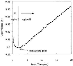
HE application of high electrical field to gate oxide, as used for Fowler–Nordheim (FN) tunneling, induces a degradation of this oxide film due to the generation of interface states, positive and negative charges in the oxide. It is observed that the magnitude of applied gate voltage, during constant current stress of FN tunneling, decreases at lower injection electron fluences and then begins to increase when the voltage goes through a minimum point [1]–[4]. A typical example of the variation of applied gate voltage during constant FN tunneling current stress is shown in Fig. 1. Positive charge trapping dominates during the initial period of current stressing which is denoted as region I in Fig. 1. Followed by the region I, the region II is dominated by the negative charge trapping. The positive charges in the oxide films of MOS capacitors have been largely studied [5]–[13] and have been found that they can be charged/discharged [10], [14]–[16]. To discharge (or relax) the positive charges without any applied voltage takes several minutes or more [17], [18].The charging/discharging phenomena can be explained by the flow of electrons in and out of traps generated by the high field stress [14]. It is also found that the flat-band voltage recovery shows a logarithmic dependence in the time regime [10]. In previous studies [6], [10], [14], [16], the flat-band voltage shift and midgap voltage variations are usually used
Manuscript received February 27, 1997; revised December 1, 1997. The review of this paper was arranged by Editor M. Fukuma. This work was supported by the National Nano Devices Laboratory under NSC 86-2215-E-009-047.
The authors are with the Department of Electronics Engineering and Institute of Electronics, National Chiao-Tung University, Hsinchu, Taiwan, R.O.C.
Publisher Item Identifier S 0018-9383(98)05257-5.
Fig. 1. The variation of gate voltage with stress time during constant 60 mA/cm2FN stress of substrate injection.
to demonstrate the discharging effect. It is also found [6] that if the first stress current of constant FN tunneling is larger than the following second stress current, the magnitude of applied gate voltage during the second FN stress will increase. However, the magnitude of the applied gate voltage shifts and their relationship with positive charges, after different relaxation times, are still not observed.
In this paper, we use the magnitude of applied gate voltage shifts during different constant FN current stresses, after positive charges generated and discharged, to demonstrate the relaxation phenomena. The positive charges formation and relaxation (discharging) are studied for two injection polarities (i.e., injections from the gate and from the substrate). We find that there is also a logarithmic dependence between the and the relaxation time. Moreover, the logarithmic dependence can derive the relationship of transient discharging currents, that flow through the oxides after removal of the stress voltage, with the relaxation time and would be proportional to which can be also derived from the tunneling front model. The effects of oxide fields (lower than the necessary voltage for FN tunneling) and wafer temperatures (373 and 423 K) for the relaxation of positive charges are also studied.
II. EXPERIMENTS
A. Device Fabrication
The devices used in this study were n polysilicon gate MOS capacitors fabricated on n-type (3–5 -cm) and p-type
(8–11 -cm) wafers using standard LOCOS isolation, with a field oxide of 400-nm thickness. A 25-nm sacrificial oxide was then grown and stripped. The gate oxides of 8 nm thickness
were grown in diluted dry O N O at 900 C
A 300 nm thickness polysilicon film was deposited by low pressure chemical vapor deposition (LPCVD), and doped n at 875 C from POCl source for 30 min. Then, a 500 nm thickness Al film was deposited by thermal evaporation and patterned. The backsides of wafers were also deposited 500 nm thickness Al films. It has been shown that the -related species degrade gate oxide film [19], therefore, the post metal-lization annealing (PMA) was done in N ambient at 400 C for 30 min to minimize hydrogen incorporation into gate oxide. The capacitor areas were cm with circular shapes. All devices were tested in accumulation regions. This means that substrate injection was performed on n-type wafers and gate injection was performed on p-type wafers to avoid the effect of white lights which were needed when the devices were tested at inversion regions. The gate oxide thicknesses were determined from ellipsometric measurements and were consistent with the C-V measurements.
B. Electrical Measurements
First, the samples were stressed at larger FN tunnel-ing constant current density, which was denoted as (100 mA/cm ), to the turn-around point (0.1 C/cm ) to ensure more positive charges generated and less negative charges generated in the oxide. The injections were performed either from the gate or from the substrate. Then the stressed samples were stressed again with smaller constant current FN tunneling density, which was denoted as (0.1 or 10 mA/cm ) after the relaxation of 10, 10 , 10 , and 10 s, to reveal the properties of traps generated by During the period of relaxation, there is no gate voltage applied. On the other hand, different temperatures (373 and 423 K) were used during FN stress and relaxation periods to investigate the temperature effects. The applied gate voltage shifts during stress were used to demonstrate the relaxation (discharging) phenomena.
After stresses, for both injection polarities, we applied 4 MV/cm constant field (no FN tunneling injection hap-pened) for 20 s. Then the samples were stressed by to investigate the effect of oxide field for positive charge relaxation.
The applied gate voltage shifts and the transient current were measured using a HP 4145B semiconductor parameter analyzer and a HP 4140B pA meter, respectively.
III. RESULTS AND DISCUSSION
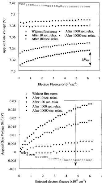
A. The Relationship Between and Relaxation Time After the generation of positive charges by (100 mA/cm ) stressing and waiting for 10, 10 , 10 , and 10 s to relax the positive charges, (0.1 mA/cm ) was performed to investigate the relaxation phenomenon. Fig. 2(a) shows the variation of applied gate voltage for substrate injection during stress. The gate voltage shift
Fig. 2. (a) The variations of applied gate voltage in stress time regime during
Imeas(0.1 mA/cm2) stress of substrate injections. The curves are withoutIgen
(100 mA/cm2from substrate) stress, withIgenstress but relaxed of 10, 103, and 104s after theIgenstress. The value of1VFNis defined in the figure. (b) The variations of applied gate voltage shift in stress time regime duringImeas
(0.1 mA/cm2) stress of substrate injections. The data are from Fig. 2(a).
used in our study is defined as the difference of gate voltage at the end of stress, in which the gate voltage seems to saturate, and at the start point of the stress. If the investigation is from the viewpoint of applied gate voltage shift, as shown in Fig. 2(b), a trend of the shifts can be observed. The arrow line in Fig. 2(b) indicates this trend which is from positive to negative when relaxation time increases. If the stress (0.1 mA/cm ) is quickly performed, the gate voltage ( ) shift is positive which means some injected electrons are trapped in the oxide [6]. However, if the are performed after a longer relaxation time passed, the gate voltage shift becomes negative. This indicates that some positive charges are compensated in relaxation period.
It is believed that if the stress voltage is removed and there is no other applications of gate voltage to oxide film, the positive charges can be compensated (discharged) by the electrons tunneling from the electrode into the charged sites
[10], [14]. The amount of compensated positive charges is increased with relaxation time. Hence, the gate voltage shifts are from positive to negative and close to the value which is without the stress.
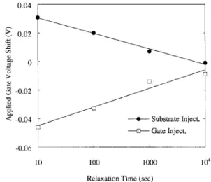
The variations of with relaxation time for gate and substrate injections are plotted in Fig. 3. It can be found that has a logarithmic dependence in the relaxation time regime. The relation can be written as
(1) in which , , and are the applied gate voltage shift, the relaxation time, and the time constant when is zero, respectively. is the slope of the curve which reveals the relaxation rate of positive charges. Positive sign is for gate injection and negative sign is for substrate injection. The values of for gate injection (p-type wafers) and substrate injection (n-type wafers) are 0.013 and 0.01, respectively. The relaxation rate of gate injection stress is slightly larger than that of substrate injection stress. Injection of electrons from poly-Si may cause more damage than from the Si substrate [21]. Hence, the energy levels, centroid or density of positive traps for gate injection are different from those for substrate injection, and different relaxation properties are revealed.
The shifts of can be written in terms of the charge densities and their locations in the following way [1]:
for substrate injection (2a) for gate injection (2b) where , and are the positive charge density per unit area, oxide permitivity, oxide thickness and the charge location, respectively. Equations (1)–(2) yield
for substrate injection (3a) for gate injection
(3b) If is about constant, then we can find the discharging current
for substrate injection (4a) for gate injection (4b) The discharge current has a dependence which is the same as the results derived from tunneling front model [22]. In other words, the variation of , as seen in Fig. 2(b), is due to the discharging of trapped charges in oxide film. We have taken (4) to simulate the transient discharging current. The is chosen as 5 nm for gate injection and oxide dielectric constant is 3.9. Fig. 4 shows the transient current of MOS capacitors after (100 mA/cm ) stress and the simulated results from (4b). It is found that the simulated results and the experimental results are matched well. Moreover, it is known that the flat-band
Fig. 3. The variation of1VFNin the relaxation time regime.
Fig. 4. The transient current through 8 nm thick oxide after 100 mA/cm2 stress. The current simulated by (4b) is well fitted with the experimental results.
voltage shift has a logarithmic dependence with discharging time [10] and, if interface states are assumed constant in the relaxation period, a similar equation as (4) can be also derived. B. The Characteristics of Under Different Stress In previous study [6], as the , the applied gate voltage during stress increased. This was attributed to that the electrons injected by recombined with the positive charges. However, in our study, we find that the gate voltage, for , does not always increase during the following stress. Fig. 5 shows the variation with stress time when the is 10 or 100 mA/cm injected from substrate. From this figure, when is 10 mA/cm which is smaller that 100 mA/cm is negative and is different from the observation of the earlier study [6]. However, as seen in Fig. 2(b), when is 0.1 mA/cm , a positive gate voltage shift variation is observed. These results suggest that, except the stress current, the oxide field during stress, the centroid of positive charges and their energy levels may also affect the results of stress.
Fig. 5. The variation of gate voltage shift whenImeas is 10 mA/cm2or 100 mA/cm2: The Igen is 100 mA/cm2:
(a)
(b)
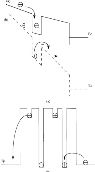
Fig. 6. (a) The schematic process of positive charge compensation during
Imeasstress. Curve (a) is for smallerImeasstress and (b) is for largerImeas
stress. (b) The schematic process of positive charge relaxation without any voltage application (see [23, Fig. 2]).
Fig. 6(a) shows the schematic processes of positive charges relaxation during Curve (a) is for smaller stress and curve (b) is for larger stress. The electrons in the
(a)
(b)
Fig. 7. (a) The curves during 0.1 mA/cm2stress at room temperature, at 373 and 423 K. The stress polarity is substrate injection. (b) The curves during
Imeas= 0:1 mA/cm2stress at room temperature, at 373 and 423 K. The stress polarity is gate injection.
oxide conduction band can be trapped into the positively charged sites. For larger measurement, the trapped electrons can easily escape from these traps by tunneling out or by crossing the trap barrier height due to the larger oxide field as shown in curve (b). Hence, the positive charges are not relaxed. However, for smaller stress, the field in oxide film is smaller and the trapped electrons hardly escape from the traps. Then the positive charges are compensated by the trapped electrons. Fig. 6(b) is the relaxation of positive charges without any gate voltage applied. It is known that the centroid of positive charges is near the electrodes [1], [4], [6], [19], [20] and can be easily discharged by the electrons tunneling from electrodes [10], [14]. Hence, the amount of relaxed positive charges become larger for longer discharging time passed. C. The Effects of Temperature and Electric Fields
Fig. 7(a) shows the stress curve at room temperature, 373 and 423 K after 10 s relaxation for substrate injection stress. Fig. 7(b) is under the same conditions of Fig. 7(a) but for gate injection stress. It can be found that is shifted to
Fig. 8. The curves duringIgen = 100 mA/cm2at room temperature and at 423 K.
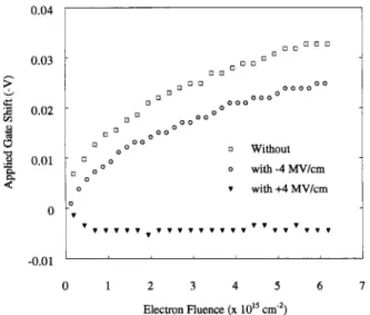
Fig. 9. The variation of gate voltage shift duringImeasstress after applica-tion of 5 MV/cm for 20 s.Igenis0100 mA/cm2andImeasis00.1 mA/cm2:
negative at higher temperature while it is positive at room tem-perature. A turn-around phenomenon reveals in Fig. 7 at 373 and at 423 K. We find that, at higher temperatures, negative charge generation process is more significant than the creation of positive charages in oxide film. Similar results at higher temperatures can be seen from the curves, in Fig. 8, during stress at different temperatures. The injection polarity in Fig. 8 is from substrate. Negative charge generation region (region II as shown in Fig. 1) has been seen at 423 K while positive charge creation (region I) is still dominated at room temperature. Turn-around point is also shifted to lower electron fluence at higher temperature. Hence, the phenomena in Fig. 7 may be due to the enhanced negative charge generation ar higher temperature. Similar results can be also observed on the gate injection stressed samples.
The effects of oxide field during positive charge relaxation are shown in Fig. 9. The injection polarity is from gate. Curve (a) is without any voltage applied, curve (b) is for 4 MV/cm applied, and curve (c) is for 4 MV/cm applied. After (100 mA/cm ) stress, we applied a field of 4 MV/cm (this
field do not form FN tunneling) to the stressed samples for 20 s. Then we apply (0.1 mA/cm ) to observe the variation of After stress, the centroid of positive charges are near the anodes [1], [6]. If the applied voltage is with the same polarity of , the relaxation of positive charges is expected to be retarded. On the other hand, if the polarity of the constant voltage is opposite to that of , the relaxation is expected to be enhanced. We find that the increase of the positive charges relaxation rate for 4 MV/cm applied is higher than that of the case for 4 MV/cm. Similar results can be also observed on the samples with substrate injection polarity. This observation is similar to the results of Lakshmanna et al. [10] and Scott et al. [14], [15].
IV. CONCLUSION
In conclusion, new relaxation phenomena of positive charges in gate oxide with FN constant current injections have been investigated and characterized. There is a logarithmic relationship between the shifts of applied FN voltage and the relaxation time. We have correlated with the transient discharging current and have derived the relationship of transient current with relaxation time which is proportional to This means that the variation of is due to the discharge of trapped charges. The result is consistent with that derived from the tunneling front model. On the other hand, under larger oxide field, electrons injected by which are trapped with positive charged sites can escape these positive traps, and the variation of is different with that under smaller oxide field. At higher temperature, negative charges are more easily generated than the positive charges. Moreover, the applied oxide field during charge relaxation can affect If the applied voltage is with the same polarity of , the relaxation of positive charges is expected to be retarded. On the other hand, if the polarity of the constant voltage is opposite to that of , the relaxation is expected to be enhanced.
REFERENCES
[1] P. Fazan, M. Dutoit, C. Martin, and M. Ilegems, “Charge generation in thin SiO2polysilicon-gate MOS capacitors,” Solid-State Electron., vol. 30, no. 8, p. 829, 1987.
[2] M. Itsumi, “Positive and negative charging of thermally grown SiO2
induced by Fowler–Nordheim emission,” J. Appl. Phys., vol. 52, p. 3491, 1981.
[3] Y. N. Cohen, J. Shappir, and D. Frohman-Bentchkowsky, “Charactr-tization of simulation bulk and interface high-field trapping effects in SiO2,” in IEDM Tech. Dig., 1983, p. 182.
[4] M. S. Liang, C. Chang, Y. T. Yeow, and C. Hu, “MOSFET degradation due to stressing of thin oxide,” IEEE Trans. Electron Devices, vol. ED-31, p. 1238, July 1984.
[5] P. S. Ku and D. K. Schroder, “Charges trapped throughout the oxide and their impact on the Fowler–Nordheim current in MOS devices,” IEEE
Trans. Electron Devices, vol. 41, p. 1669, Sept. 1994.
[6] Y. Nissan-Cohen, J. Shappir, and D. Frohman-Bentchkowsky, “High field current induced-positive charge transients in SiO2,” J. Appl. Phys., vol. 54, p. 5793, 1983.
[7] , “High-field and current-induced positive charge in thermal SiO2
layers,” J. Appl. Phys., vol. 57, p. 2830, 1985.
[8] M. V. Fischetti, Z. A. Weinberg, and J. A. Calise, “The effect of gate metal and SiO2 thickness on the generation of donor states at the Si-SiO2interface,” J. Appl. Phys., vol. 57, p. 418, 1985.
[9] D. J. DiMaria, D. Arnold, and E. Cartier, “Impact ionization and positive charge formation in silicon dioxide films on silicon,” Appl. Phys. Lett., vol. 60, p. 2118, 1992.
[10] V. Lakshmanna and A. S. Vengurlekar, “Logarithmic detrapping re-sponse for holes injected into SiO2 and the influence of thermal activation and electric fields,” J. Appl. Phys., vol. 63, p. 4548, 1988. [11] S. Elrharbi, M. Jourdain, and A. Meinertzhagen, “Effect of tunneling
electrons in Fowler–Nordheim regime on the current–voltage char-acteristics and model of degradation of metal-oxide-semiconductor capacitors,” J. Appl. Phys., vol. 76, p. 1013, 1994.
[12] S. E. Thompson and T. Nishida, “Positive charge generation in SiO2by electron-impact of trapped electrons,” J. Appl. Phys., vol. 72, p. 4683, 1992.
[13] D. A. Buchanan and D. J. DiMaria, “Interface and bulk trap generation in metal-oxide-semiconductor capacitors,” J. Appl. Phys., vol. 67, p. 7439, 1990.
[14] R. S. Scott, N. A. Dumin, T. W. Hughes, D. J. Dumin, and B. T. Moore, “Properties of high-voltage stress generated traps in thin silicon oxide,”
IEEE Trans. Electron Devices, vol. 43, p. 1133, July 1996.
[15] R. S. Scott and D. J. Dumin, “The charging and discharging of high-voltage stress-generated traps in thin silicon oxide,” IEEE Trans.
Electron Devices, vol. 43, p. 130, Jan. 1996.
[16] A. Meinertzhagen, C. Petit, G. Yard, M. Jourdain, and A. Ei Hdiy, “On the positive charge and interface states in metal-oxide-semiconductore capacitors,” J. Appl. Phys., vol. 80, p. 271, 1996.
[17] M. V. Fischetti, “Generation of positive charge in silicon dioxide during avalanche and tunnel electron injection,” J. Appl. Phys., vol. 57, p. 2860, 1985.
[18] L. P. Trombetta, F. J. Feigl, and R. J. Zeto, “Positive charge generation in metal-oxide-semiconductor capacitors,” J. Appl. Phys., vol. 69, p. 2512, 1991.
[19] D. J. DiMaria and J. W. Stasiak, “Trap creation in silicon dioxide produced by hot electrons,” J. Appl. Phys., vol. 65, p. 2342, 1989. [20] D. J. DiMaria, E. Cartier, and D. Arnold, “Impact ionization, trap
cre-ation, degradcre-ation, and breakdown in silicon dioxide films on silicon,”
J. Appl. Phys., vol. 73, p. 3367, 1993.
[21] P. P. Apte and K. C. Saraswat, “Correlation of trap generation to charge-to-breakdown (Qbd): A physical-damage model of dielectric
breakdown,” IEEE Trans. Electron Devices, vol. 40, p. 512, Mar. 1993. [22] D. J. Dumin and J. R. Maddux, “Correlation of stressed-induced leakage current in thin oxides with trap generation inside the oxides,” IEEE
Trans. Electron Devices, vol. 40, p. 986, May 1993.
[23] D. J. Dumin, S. K. Mopuri, S. Vanchinathan, R. S. Scott, R. Subra-manian, and T. G. Lewis, “High field related thin oxide wearout and breakdown,” Trans. Electron Devices, vol. 42, pp. 760–772, Apr. 1995.
Kow-Ming Chang (M’88) received the B.S. degree
(with Great Distinction) in chemical engineering from National Central University, Chung-Li, Tai-wan, R.O.C., in 1977, and the M.S. and Ph.D. degrees in chemical engineering from the Univer-sity of Florida, Gainesville, in 1981 and 1985, respectively. His doctoral research concerned the processing technologies of compound semiconduc-tors.
In 1985, he joined the Department of Electronics Engineering and Semiconductor Research Center, National Chiao-Tung University, Hsinchu, Taiwan, where he is currently a Professor. From 1989 to 1990, he was a Visiting Professor in the Electrical Engineering Department, University of California, Los Angeles, where he was engaged in research on the system design of electron cyclotron resonance chemical vapor deposition (ECR-CVD) for developing the low-temperature processing technology. He was in charge of a 500 keV ion implanter, selective tungsten LPCVD system, and two UHV-ECR-CVD systems installed in National Nano Device Laboratory (NDL) at the National Chiao-Tung University. His current research interests are in the physics, technologies, and modeling of heterojunction devices and optoelectronic devices, ULSI key technologies, CMOS devices, and MEMS technologies. He has published over 80 articles in these fields and has served as a reviewer for international journals such as IEEE ELECTRON DEVICE LETTERS and the Journal of the
Electrochemical Society.
Dr. Chang is member of Phi Tau Phi, AIChE, and the Electrochemical Society.
Chii-Horng Li was born in Taipei, Taiwan, R.O.C.,
in 1969. He received the B.S. degree from the Department of Electronics Engineering, National Chiao-Tung University, Hsinchu, Taiwan, in 1992. He is currently pursuing the Ph.D. degree in the Institute of Electronics, National Chiao-Tung Uni-versity. His research interests include fabrication technology and reliability of thin gate oxides.
Shih-Wei Wang was born in Pingtone, Taiwan,
R.O.C., on December 25, 1969. He received the B.S. degree in electrical engineering from National Central University, Chung-Li, Taiwan, in 1992, and the Ph.D. degree from the Institute of Electronics, National Chiao-Tung University, Hsinchu, Taiwan, in 1997. His research interests are in the areas of the metallization and intermetal dielectric fabrica-tion technology and reliability for VLSI back-end process.
Ta-Hsun Yeh was born in Taiwan, R.O.C., on
August 14, 1967. He received the B.S. degree in electrical engineering from National Central Uni-versity, Chung-Li, Taiwan, in 1989, and the Ph.D. degree in electronics engineering from National Chiao-Tung University, Hsinchu, Taiwan, in 1997. His research interests include the CVD-W process and related metallization technologies for ULSI applications.
Ji-Yi Yang was born in Taoyuan, Taiwan, R.O.C.,
in 1969. He is currently pursuing the Ph.D. degree in the Institute of Electronics, National Chiao-Tung University, Hsinchu, Taiwan. His research interests include retrograde well MOS design and the fabrica-tion of low dielectric constant intermetal dielectrics.
Tzyh-Cheang Lee was born in Chia-ii, Taiwan,
R.O.C., on November 12, 1968. He received the B.S. degree in electrical engineering from National Taiwan University, Taipei, in 1992. He is currently purusing the Ph.D. degree in the Institute of Elec-tronics, National Chiao-Tung University, Hsinchu, Taiwan. His research interests are in the areas of dielectric reliability.