This content has been downloaded from IOPscience. Please scroll down to see the full text.
Download details:
IP Address: 140.113.38.11
This content was downloaded on 28/04/2014 at 02:36
Please note that terms and conditions apply.
Nanomechanical properties of lead zirconate titanate thin films by nanoindentation
View the table of contents for this issue, or go to the journal homepage for more 2003 J. Phys.: Condens. Matter 15 5253
(http://iopscience.iop.org/0953-8984/15/30/307)
INSTITUTE OFPHYSICSPUBLISHING JOURNAL OFPHYSICS:CONDENSEDMATTER
J. Phys.: Condens. Matter 15 (2003) 5253–5259 PII: S0953-8984(03)56149-5
Nanomechanical properties of lead zirconate titanate
thin films by nanoindentation
Te-Hua Fang1,3, Sheng-Rui Jian2and Der-San Chuu2
1Department of Mechanical Engineering, Southern Taiwan University of Technology,
Tainan 710, Taiwan
2Institute and Department of Electrophysics, National Chiao Tung University, Hsinchu 300,
Taiwan E-mail: [email protected] Received 15 November 2003 Published 18 July 2003 Online atstacks.iop.org/JPhysCM/15/5253 Abstract
The nanomechanical properties of lead zirconate titanate (PZT) thin films were subjected to nanoindentation evaluation. A PZT thin film was created on a silicon substrate by radio frequency magnetron sputtering. The structure and surface morphology were analysed by x-ray diffraction and atomic force microscopy. Results show that PZT thin films were well ordered with a high (110) orientation and presented a pure perovskite-type structure and that the average roughness was reduced as the annealing temperature was increased. The Young’s modulus and hardness increased as the rapid annealing temperature increased from 600 to 800◦C, with the best results being obtained at 800◦C. (Some figures in this article are in colour only in the electronic version)
1. Introduction
In recent years, ferroelectric thin films such as lead zirconate titanate (PZT) have attracted a lot of attention from their use in dynamic random access memory (DRAM), non-volatile ferroelectric random access memory (FRAM), micro-electromechanical systems (MEMS) and optical modulators due to their high dielectric constants, piezoelectric and pyroelectric properties, and good electro-optical characteristics [1–4].
Much attention is also being paid to the study of surface nanomechanical properties, because the success of many applications is partly determined by a precise understanding of these characteristics. Understanding the nanomechanical properties is especially important for films used to create MEMS. As a general rule, the performance of these surface and near-surface nanomechanical properties dominates the overall performance of the bulk material.
3 Author to whom any correspondence should be addressed.
5254 T-H Fang et al
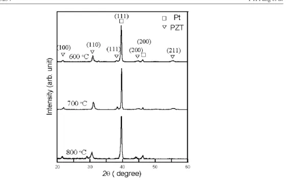
Figure 1. The XRD patterns of PZT films on Pt/Ti/SiO2/Si substrates annealed at different
temperatures, ranging from 600 to 800◦C.
Table 1. The deposition condition for PZT thin films. Sputtering method RF magnetron sputtering Target PZT ceramic target 4 inch∅ Substrate Pt/Ti/SiO2/Si
RF power 100 W
Base pressure of system 1.0 × 10⁻⁵Torr Sputtering gas (Ar) pressure 5.0 × 10⁻³Torr Film thickness 500 nm
Consequently, the measurement and understanding of these surface-related properties is of prime importance for the practical application of various systems in various environments.
For measuring the properties of thin films, such as Young’s modulus and hardness on the nanoscale, nanoindentation is the most frequently used technique [5–7]. Research in this area is partially summarized in [8–11].
This study presents the results from a scanning nanoindentation system that operates in the conventional mode and employs a Berkovich indenter to investigate the nanomechanical characteristics of PZT thin films. The microstructural properties are characterized by x-ray diffraction (XRD) and the surface morphology by atomic force microscopy (AFM). The influence of the rapid thermal annealing (RTA) of PZT thin films is also presented.
2. Experiment details
PZT thin films were deposited by RF magnetron sputtering using a 4 inch ceramic PZT target of Pb(Zr0.52Ti0.48)O3. A 500 nm thick film was produced in a single coating process. The RF
power was set at 100 W and the system base pressure was set to 1.0 × 10⁻⁵Torr. The growth conditions are listed in table 1.
Nanomechanical properties of PZT thin films by nanoindentation 5255
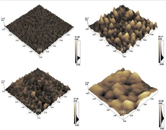
Figure 2. (a)–(d) AFM images of PZT thin films in the initial virgin state and at annealing temperatures of 600, 700 and 800◦C, respectively. The surface region has an area of 1µm2.
The substrate was a Si(100) wafer coated with 900 nm of SiO2, then 20 nm of Ti and
lastly 200 nm of Pt. The SiO2layer was deposited by wet thermal oxidation and the Ti and Pt
films were deposited by RF magnetron sputtering using argon (Ar) as the sputtering source. Following PZT deposition, and to induce the perovskite phase within the films, RTA was carried out for 2 min at different temperatures between 600 and 800◦C. RTA processing of the PZT thin films decreased the surface energy via thermal-treatment mechanisms and reduced the film’s surface irregularities, i.e. crystalline grains.
After RTA processing, the resulting PZT thin film’s microstructural properties were analysed by XRD (using a Rigaku D/Max2500 from Rigaku/MSC Inc. of the USA, with Cu Kα radiation). The crystallographic orientation was determined by XRD rotation over θ–2θ degrees. Use of a rotating diffractometer is beneficial in generating PZT film diffractograms free of substrate peaks, such as (111) Pt peaks [12, 13]. After that, the specimens were scanned by AFM (using an SPM-9500J2 from Shimadzu of Japan) for morphological surface properties. For each AFM operation, a constant scan speed of 1µm s−1was used, with a constant load of 30 nN applied to the cantilever.
Nanomechanical properties, such as Young’s modulus and hardness, were obtained by nanoindentation (using a Triboscope from Hysitron Inc. of the USA). Load-controlled indentation testing followed a trapezoidal loading profile with a 10 s typical peak load hold time. The peak loads ranged from 1000 to 2000µN at a loading rate of 10 µN s−1. The diamond indenter was a Berkovich tip with a tip radius of 100 nm [6].
5256 T-H Fang et al
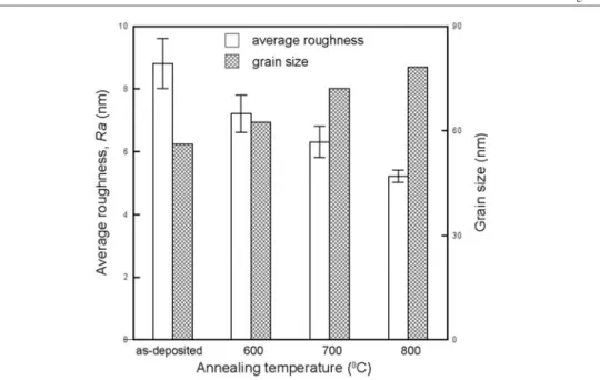
Figure 3. The average roughness, Ra, and grain size as a function of the annealing temperature
for PZT films.
3. Results and discussion
It was found that a film’s microstructure and orientation were both very sensitive to the temperature of RTA. As seen in figure 1, XRD analysis revealed crystallographic and orientational differences between test samples annealed at 600, 700 and 800◦C. All three films contained only the perovskite phase, i.e. there was no observable pyrochlore phase in the range of annealing temperatures used. This might have been because the heating rate of the RTA process was so high that the temperature passed through the range of pyrochlore formation temperature too quickly to nucleate. The PZT thin films exhibited a pyrochlore phase when the annealing temperature was lower. The results demonstrated that a pure perovskite-phase PZT thin film could be deposited directly onto a Pt/Ti/SiO2/Si substrate by RF sputtering
followed by an RTA process using temperatures that ranged from 600 to 800◦C. The quality of the films was high, as demonstrated by the orientation-selective surface structure (i.e. (110) PZT and (111) Pt).
AFM was used to analyse the PZT thin film’s surface asperity at various annealing temperatures. Figure 2 shows the surface topography for PZT thin films: (a) as deposited, and at annealing temperatures of (b) 600, (c) 700 and (d) 800◦C. The surface grain structure can be seen in all the samples. However, the number of grains and voids in figures 2(b) and (c) were larger than in figure 2(d). Importantly, the surface in figure 2(d) appears smooth and void-free, i.e. the grains were well crystallized and homogeneously distributed and demonstrate that there was surface improvement at an annealing temperature of 800◦C.
The Scherrer formula [14] was adopted to estimate the mean grain size of the PZT films from the measured width of their diffraction curves. The mean grain sizes of the films were 62.38, 72.05 and 78.24 nm for annealing temperatures of 600, 700 and 800◦C, respectively, and are illustrated in figure 3. It can be observed that the grain size of PZT films increased as the annealing temperature was increased.
Nanomechanical properties of PZT thin films by nanoindentation 5257
Figure 4. The load-displacement curve and the indent AFM image of PZT thin film at an annealing temperature of 600◦C.
The average roughness, Ra, of the PZT films is shown in figure 3. The above-mentioned
results for mean grain size indicated that the grain size increased as the annealing temperature was increased, although the average roughness values decreased. The larger grained and more uniform microstructure appeared at the highest annealing temperature and had a more pronounced preferential orientation.
Figure 4 illustrates the results of the depth-sensing nanoindentation testing on the PZT film annealed at 600◦C. A triangular indentation was clearly seen in the AFM micrograph, with additional pile-up around the indentation giving further evidence of plastic behaviour. This ‘pile-up’ phenomenon is found to be anisotropic, i.e. the magnitude of the pile-up increased as the indentation load was increased.
The area/depth relation for a Berkovich indenter is
Ac= 24.56h2 (1)
where Acis the contact area, h is the calculated indentation depth, and the constant assumes a
perfectly manufactured tip with a face angle of 65.3◦. The contact area Acis calculated from
stiffness values obtained from the nanoindentation data. In depth-sensing nanoindentation, the relationship between the stiffness and contact area is given by
S = β2
√
Ac
π E∗ (2)
5258 T-H Fang et al
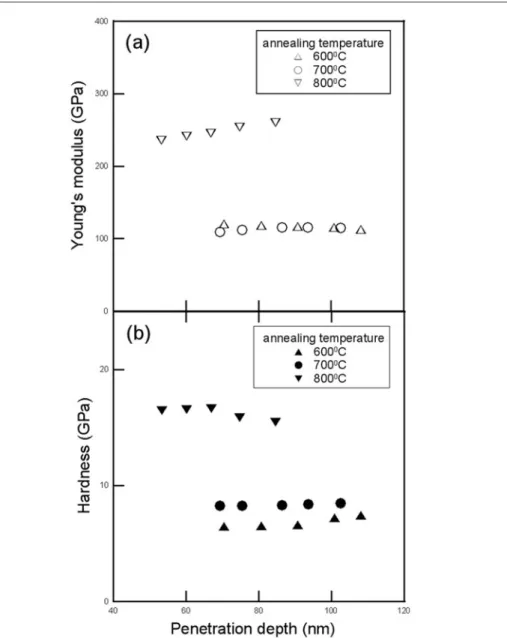
Figure 5. (a) Young’s modulus and (b) the hardness as a function of penetration depth for PZT films annealed at 600, 700 and 800◦C.
The composite modulus E∗is, from [6], 1 E∗ = 1− ν2 i Ei + 1− ν 2 m Em (3) whereν and E are Poisson’s ratio and Young’s modulus, respectively, and the subscripts i and m refer to the indenter and test material. The indenter properties used in this study’s calculations were Ei= 1140 GPa and νi= 0.07, assuming that νm= 0.25.
The PZT thin film’s Young’s modulus can be derived during nanoindentation by equations (2) and (3), as mentioned above. The Young’s moduli obtained from nanoindentation at different applied loads are shown in figure 5(a) and ranged from 109.17 to 260.04 GPa.
Nanomechanical properties of PZT thin films by nanoindentation 5259 Young’s modulus differed according to annealing temperatures and indentation depths due to the appreciable substrate effects at greater indentation depths.
The hardness of a material is defined as its resistance to local plastic deformation. Thus, hardness H is determined from the maximum indentation load, Pmax, divided by the actual
projected area of contact [6]:
H= Pmax Ac
. (4)
Figure 5(b) shows the hardness/penetration depth plots for PZT films, with hardness ranging from 6.49 to 16.63 GPa. The hardness increased as the annealing temperature was increased, with maximum hardness being obtained at 800◦C. Clearly the increased hardness coincided with the structural and phase changes found in figure 1. Figure 5 shows that Young’s modulus was at it’s maximum at 800◦C, so it is safe to conclude that 800◦C was the preferred RTA temperature.
4. Conclusion
XRD, AFM and nanoindentation techniques have been used to investigate the surface features of PZT thin films produced by a sputtering deposition process and followed by RTA.
XRD analysis showed that the PZT thin film had a predominant (110) orientation, a pure perovskite-type configuration and a smoother surface morphology at higher annealing temperatures.
Young’s modulus ranged from 109.17 to 260.04 GPa and hardness ranged from 6.49 to 16.63 GPa for annealing temperatures of 600, 700 and 800◦C.
In summary, nanoindentation has established on the nanoscale the Young’s modulus and hardness of the PZT thin film, as well as various other characteristics such as the preferred RTA treatment for maximum hardness, the variation in crystallographic orientation as the annealing temperature was increased, and the presence of a pure perovskite-type structure within the as-deposited film and at all annealing temperatures.
Acknowledgment
This work was partially supported by the National Science Council of Taiwan under grant nos NSC91-2218-E218-001 and NSC91-2212-E-218-007.
References
[1] Watanabe S, Fujiu T and Fuji T 1995 Appl. Phys. Lett. 66 1481 [2] Land C E 1989 J. Am. Ceram. Soc. 72 11
[3] Nagashima K, Hirai T, Koike H, Fujisaki Y and Tarui Y 1996 Japan. J. Appl. Phys. 35 1680 [4] Auciello O, Scott J F and Ramesh R 1998 Phys. Today 51 22
[5] Pethica J B, Hutchings R and Oliver W C 1983 Phil. Mag. A 48 593
[6] Moody N R, Gerberich W W, Burnham N and Baker S P 1998 Fundamentals of Nanoindentation and Nanotribology (Warrendale, PA: Materials Research Society)
[7] Yang C M 1995 Mater. Chem. Phys. 41 295
[8] Fougere G E, Riester L, Ferber M, Weertman J R and Siegel R W 1995 Mater. Sci. Eng. A 204 1 [9] Hung Z, Gu L Y and Weertman J R 1997 Scr. Mater. 37 1071
[10] Oliver W C and Pharr G M 1992 J. Mater. Res. 7 1564
[11] Doerner M F, Gardner D S and Nix W D 1986 J. Mater. Res. 7 845
[12] Zeng J, Wang L, Gao J, Song Z, Zhu X, Lin C, Hou L and Liu E 1999 J. Cryst. Growth 197 874 [13] Hector J, Floquet N, Niepce J C, Gaucher P and Ganne J P 1995 Microelectron. Eng. 29 285 [14] Cullity B D 1978 Elements of X-ray Diffraction (Reading, MA: Addison-Wesley) p 102