Recovering Dielectric Loss of Low Dielectric Constant Organic
Siloxane during the Photoresist Removal Process
T. C. Chang,a,c,
*
,zY. S. Mor,bP. T. Liu,cT. M. Tsai,bC. W. Chen,bY. J. Mei,d and S. M. Szeb,c
a
Department of Physics, National Sun Yat-Sen University, Kaohsiung, Taiwan bInstitute of Electronics, National Chiao Tung University, Hsin-Chu, Taiwan c
National Nano Device Laboratory, Hsin-Chu 300, Taiwan
dDepartment of Electrical Engineering, Ching-Yun Institute of Technology, Jung-Li, Taiwan
The interaction between low dielectric constant共low-k兲 hybrid organic siloxane polymer 共HOSP兲 and O2plasma ashing has been investigated. O2 plasma ashing is commonly performed to remove the photoresist共PR兲 during integrated circuit fabrication. However, dielectric loss usually occurs in the HOSP films during the PR removal process. In order to eliminate dielectric loss originating from an O2plasma attack, hexamethyldisilazane共HMDS兲 treatment is proposed to repair the damage in the HOSP film. HMDS can react with Si-OH bonds and reduce moisture uptake. Moreover, the leakage current and the dielectric constant is decreased significantly when damaged HOSP film undergoes HMDS treatment. For this reason, HMDS treatment is a promising method to apply to the photoresist removal.
© 2002 The Electrochemical Society. 关DOI: 10.1149/1.1485776兴 All rights reserved. Manuscript received September 20, 2001. Available electronically June 12, 2002.
As the device dimensions continue to shrink to 0.25 m and below, the interconnect delay becomes a limiting factor for increas-ing device speed. Since the RC delay is a product of the resistance in the metal interconnect 共R兲 and the capacitance between the metal lines 共C兲, incorporating new materials of low resistivity and low permittivity into interconnect fabrication can effectively reduce this time constant.1,2
In order to decrease the resistance共R兲, copper has recently been introduced as an interconnect metal, due to its high electrical con-ductivity. In addition, the low dielectric constant共low-k兲 materials are also proposed for decreasing the parasitical capacitor for future integrated circuit共IC兲 applications.3-9 One of the promising low-k dielectrics, a spin-on deposition hybrid organic siloxane polymer 共HOSP兲 is a strong candidate. The HOSP is derivative of SiO2, in which one of the four oxygen atoms bonded to every silicon atom is replaced by hydrogen and methyl groups. In addition, the HOSP has a low dielectric constant of about 2.5 so that it has a high evaluation in ultralarge scale integration共ULSI兲 applications.
However, photoresist stripping is an indispensable step in inte-gration processing. The dielectric properties of the HOSP films will degrade after photoresist stripping.10,11As a result, hexamethyldisi-lazane共HMDS兲 treatment is proposed for improving the quality of the HOSP film after photoresist stripping. Furthermore, electrical measurements and material analyses have also been used to evaluate the HOSP film during the photoresist stripping process.
Experimental
The wafers were coated with the HOSP solution at a rotation of 500 rpm for 5 s, and the sequential spin was at 2500 rpm for 20 s. After the spin-coating process, the HOSP films were baked on a hot plate at 150, 200, and 350°C for 1 min, respectively. Finally, the resulting wafers were further processed by furnace curing at 400°C under nitrogen ambient for 1 h.
In this work, samples STD, A, and B were prepared. Sample STD was the as-cured HOSP film without any plasma treatment. Sample A was the HOSP film with O2 plasma ashing for 1 min. Sample B was the O2 plasma-treated HOSP film共sample A兲 after having undergone an HMDS atmosphere at 80°C for 15 min. After-ward, aluminum were deposited on samples STD, A, and B as the top electrode to manufacture the metal insulation semiconductor 共MIS兲 structure.
The O2 plasma ashing was carried out at a plasma-enhanced chemical vapor deposition chamber. The O2 plasma was operated with a rf power of 200 W at a pressure of 300 mTorr. The flow rate was 700 sccm, and the operating temperature was kept at 300°C.
The chemical bonds of the HOSP films after different processes were investigated by Fourier transform infrared 共FTIR兲 spectros-copy. The thickness of the HOSP films was measured by an N&K analyzer. The thermal desorption system spectrometer 共TDS兲 was carried out to monitor the desorbed moisture from HOSP films. A Keithley model 82 C-V meter was used to measure the dielectric constant of HOSP films, and the capacitance-voltage (C-V) charac-teristics were measured at 1 MHz with an ac bias for high frequency. Finally, the current-voltage (I-V) characteristics were also measured using a MIS structure to evaluate the insulation property of HOSP films.
Results and Discussion
In the integrated processes, photoresist removal is an indispens-able step. The photoresist removal is implemented conventionally by utilizing O2plasma ashing. Therefore, the impact of O2plasma ash-ing on the quality of HOSP film is investigated in this study. Figure 1 shows the thickness variation of HOSP film共sample STD兲 with O2 plasma ashing for 1 to 9 min. The thickness of the HOSP film is decreased with an increase of the O2 plasma treatment time. The film shrinkage is due to the damaged structure after the HOSP film undergoes the O2 plasma ashing process. The FTIR spectra have confirmed our inference. Figure 2 shows the FTIR spectra of the HOSP film with O2plasma ashing for 1 to 9 min. The intensity of Si-OH bonds and H2O is increased after O2plasma ashing. Further-more, the intensities of Si-H, C-H, and Si-CH3peaks are decreased dramatically. During O2plasma ashing, the oxygen radicals can dif-fuse into the HOSP film to attack the functional groups and conse-quently a large amount of Si-CH3bonds and Si-H bonds are broken. This will cause the HOSP films to generate dangling bonds. The dangling bonds may be easily converted into Si-OH bonds when the dangling bonds are exposed to the environment. The Si-OH bonds in the damaged HOSP films often lead to moisture uptake with the result that the Si-OH bonds and H2O signal appear in the FTIR spectra.
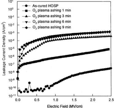
Figure 3 shows the leakage current density of the HOSP film with O2 plasma ashing for 1 to 9 min. The leakage current is in-creased with the increase of the O2plasma treatment time. Further-more, the dielectric constant is also increased with the increase of the O2plasma treatment time, as shown in Fig. 4. The dielectric loss *Electrochemical Society Active Member.
zE-mail: tcchang@ndl.gov.tw
Journal of The Electrochemical Society, 149共8兲 F81-F84 共2002兲
0013-4651/2002/149共8兲/F81/4/$7.00 © The Electrochemical Society, Inc.
F81
) unless CC License in place (see abstract).
ecsdl.org/site/terms_use
address. Redistribution subject to ECS terms of use (see
140.113.38.11
is due to the destruction of functional groups in the HOSP films after the O2 plasma ashing process, which is consistent with the FTIR spectra in Fig. 2.
In order to overcome these issues, HMDS treatment has been developed to repair the damage originating from photoresist stripping in the HOSP film. Chemical HMDS treatment, (CH3)3Si-NH-Si(CH3)3, can react with Si-OH bonds caused by O2 plasma ashing in the damaged HOSP film. The chemical reaction equation between the HMDS and Si-OH bonds is shown as follows12
共CH3兲3Si-NH-Si共CH3兲3共g兲⫹ HO-Si-共s兲→ 共CH3兲3-Si-O-Si-共s兲
⫹ 共CH3兲3-SiNH2共g兲 关1兴
共CH3兲3-SiNH2共g兲⫹ HO-Si-共s兲→ 共CH3兲3-Si-O-Si-共s兲⫹ NH3共g兲 关2兴 Figure 5 shows FTIR spectra of samples STD, A, and B. When sample A undergoes HMDS repair, the intensity of the Si-OH bonds and moisture decreases, as shown in sample B. These experimental Figure 1. The thickness variation of HOSP films共sample STD兲 with O2
plasma ashing for 1 to 9 min.
Figure 2. The FTIR spectra of HOSP films共sample STD兲 with O2plasma
ashing for 1 to 9 min.
Figure 3. The leakage current density of HOSP films共sample STD兲 with O2
plasma ashing for 1 to 9 min.
Figure 4. The dielectric constant of HOSP films共sample STD兲 with O2
plasma ashing for 1 to 9 min.
Journal of The Electrochemical Society, 149共8兲 F81-F84 共2002兲 F82
) unless CC License in place (see abstract).
ecsdl.org/site/terms_use
address. Redistribution subject to ECS terms of use (see
140.113.38.11
results are consistent with our inference. The Si-OH bonds not only are decreased to repair the damaged HOSP film, but react with HMDS to form Si-OSi(CH3)3bonds. The Si(CH3)3bonds are hy-drophobic so that the film surface can be made more hyhy-drophobic by HMDS treatment.
The hydrophobic surface will reduce the moisture uptake. The TDS analysis also confirms our inference, as shown in Fig. 6. The moisture content of sample B is significantly lower than that of sample A. These results indicate that HMDS treatment of HOSP film
can effectively enhance the resistance to moisture uptake, and for this reason the dielectric property of HOSP film will be maintained at an excellent level.
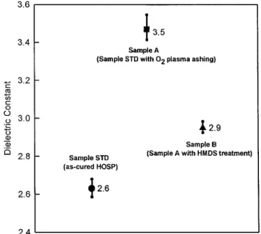
Figures 7 and 8 show both the dielectric constant and leakage current variations when HOSP film undergoes O2plasma ashing and HMDS treatment. The dielectric constant of HOSP will increase after O2 plasma ashing, whereas it will decrease after sequential HMDS treatment. The dielectric constant of sample STD increases from 2.6 to 3.5 after O2plasma ashing, as shown in sample A. After sequential HMDS treatment, the dielectric constant reduces to 2.9, as shown in sample B.
Moreover, the leakage current density increases significantly when sample STD undergoes O2plasma ashing, as shown in sample Figure 5. The FTIR spectra of sample STD, sample A, and sample B.
Figure 6. The temperature dependence of moisture desorption of sample
STD, sample A, and sample B.
Figure 7. The dielectric constant of sample STD, sample A, and sample B.
Figure 8. The leakage current density of sample STD, sample A, and sample
B.
Journal of The Electrochemical Society, 149共8兲 F81-F84 共2002兲 F83
) unless CC License in place (see abstract).
ecsdl.org/site/terms_use
address. Redistribution subject to ECS terms of use (see
140.113.38.11
A. After further HMDS treatment, the leakage current density is decreased by a factor of 1-2, as shown in sample B. This indicates that HMDS can repair the damaged structure in the HOSP film and reduce both the leakage current density and dielectric constant after the photoresist removal process.
Conclusions
In this study, HMDS treatment is applied to HOSP films. The HMDS treatment can eliminate the Si-OH bonds in the damaged HOSP film, transforming more hydrophobic surfaces. This can re-duce moisture uptake in the HOSP film so that the leakage current and dielectric constant will decrease. Material analyses verified our interpretation. The Si-OH bounds are decreased significantly in the FTIR spectra when the damaged HOSP film undergoes HMDS treat-ment. In addition, TDS analysis also shows that the moisture uptake can be reduced after HMDS treatment and as a consequence the dielectric properties will be maintained in excellent condition. As a result, HMDS treatment is a promising method for repairing the dielectric loss to the HOSP film in the photoresist removal process.
Acknowledgments
This work was performed at the National Nano Device Labora-tory and was supported by Honeywell Taiwan, Inc., and the National
Science Council of the Republic of China under contract no. NSC90-2112-M-110-004 and no. NSC90-2215-E-009-048.
National Sun Yat-Sen University assisted in meeting the publication costs of this article.
References
1. The National Technology Roadmap for Semiconductors, Semiconductor Industry Association, San Jose, CA共1997兲.
2. T. E. Seidel and C. H. Ting, Mater. Res. Soc. Symp. Proc., 381, 3共1995兲. 3. P. T. Liu, T. C. Chang, Y. L. Yang, Y. F. Cheng, and S. M. Sze, IEEE Trans.
Electron Devices, 47, 1733共2000兲.
4. M. G. Albrecht and C. Blanchette, J. Electrochem. Soc., 145, 4019共1998兲. 5. M. J. Loboda, C. M. Grove, and R. F. Schneider, J. Electrochem. Soc., 145, 2861
共1998兲.
6. S. W. Lin, M. Miyata, T. Naito, Y. Shimogaki, Y. NaKano, K. Tada, and H. Ko-miyama, Mater. Res. Soc. Symp. Proc., 443, 143共1996兲.
7. A. Grill, V. Patel, K. L. Saenger, C. Jahnes, S. A. Cohen, A. G. Schrott, D. C. Edelstein, and J. R. Paraszczak, Mater. Res. Soc. Symp. Proc., 443, 155共1996兲. 8. S. M. Rossnagel, in Proceedings of VLSI Multilevel Interconnection Conference
(VMIC), p. 576共1995兲.
9. S. Okuda, Y. Shioya, and H. Kashimada, in Proceedings of VLSI Multilevel Inter-connection Conference (VMIC), p. 424共1995兲.
10. P. T. Liu, T. C. Chang, Y. S. Mor, and S. M. Sze, Jpn. J. Appl. Phys., Part 1, 38, 3482共1999兲.
11. P. T. Liu, T. C. Chang, S. M. Sze, F. M. Pan, Y. J. Mei, W. F. Wu, M. S. Tsai, B. T. Dai, C. Y. Chang, F. Y. Shih, and H. D. Huang, Thin Solid Films, 332, 345共1998兲. 12. S. V. Nitta, V. Pisupatti, A. Jain, P. C. Wayner, Jr., W. N. Gill, and J. L. Plawsky, J.
Vac. Sci. Technol. B, 17, 205共1999兲.
Journal of The Electrochemical Society, 149共8兲 F81-F84 共2002兲
F84
) unless CC License in place (see abstract).
ecsdl.org/site/terms_use
address. Redistribution subject to ECS terms of use (see
140.113.38.11