行政院國家科學委員會專題研究計畫 期中進度報告
子計畫五:針對系統設計探索之單晶片網路系統設計平台之
研究(1/3)
計畫類別: 整合型計畫 計畫編號: NSC94-2220-E-009-037- 執行期間: 94 年 08 月 01 日至 95 年 07 月 31 日 執行單位: 國立交通大學電子工程學系及電子研究所 計畫主持人: 周景揚 計畫參與人員: 王成業、林亮宇、林步青、陳冠豪 報告類型: 完整報告 處理方式: 本計畫可公開查詢 中 華 民 國 95 年 5 月 29 日1. 中文摘要 由於製程技術的進步,在單晶片系統上整合數十億電晶體需要新的設計方法以增加設 計生產力。而共用型的匯流排在複雜的資料傳輸上,會有相當的問題。因此單晶片網路系 統正是解決這個問題最主要的方法。在這個計畫裡,我們將使用網路的相關技術,結合多 處理器的環境,打造下一世代的單晶片網路系統設計發展平台。這包括交換器的設計,工 作與資源配置以及相關系統模擬等。最後也將以其他子計畫所設計之適用於行動環境及具 有多輸出入天線之無線都會網路基頻傳收機當整個設計平台之驗證機制。 本計畫的今年目標就是設計一個適用於單晶片網路系統上的交換器以及相關架構,其 相關的邏輯設計以及排程演算法均會詳加研究,此交換器所建立的網路可以保證頻寬,並 且可以有效率的處理資料。 英文摘要
As silicon technology advances, the exploitation of a billion-transistor capacity of a chip requires new system paradigms and significant improvements to design productivity. As many processors and dedicated hardware processing units can be accommodated on a single chip, many problems related to shared-bus-based communication have appeared. Network-on-Chip (NoC) is one of the best candidates for handling on-chip communication. In this project, we will study and build the essential design framework of NoC including the switch designs, the task binding algorithm and the simulation environment. We will then use the Mobil MIMO WMAN baseband transceiver designed by other subprojects as our design vehicle to exercise our NoC design framework.
The goal of this project in this year is to design the switch and the related architecture for NoC designs. The detail logic design and the related scheduling algorithm will be developed for the switch. This network built by using these switches can guarantee communication throughput and can efficiently transmit data.
2. 計畫的緣由與目的
The Network-on-Chip (NoC) paradigm is a new design methodology that meets the criteria of communication architecture of MP-SoCs designs. The NoC platforms not only provide better scalability, modularity and efficient on-chip communication but also separate the communication fabric from the processing and storage elements. Therefore, designers can exploit different levels of abstraction to optimize the communication medium and the functionality independently. As was
mentioned above, we can easily amortize the platform development cost across many applications and reduce time to market pressure by reusing the NoC platform.
3. 研究方法及成果
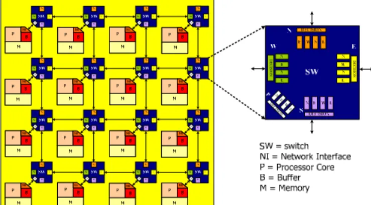
There are many different interconnection architectures of NoC platform. In this work, several assumptions are made in the following. First, without lost of generality, we assume that our interconnection architecture of the NoC platform as a mesh-based topology where the platform is exposed in Figure 1. Second, the platform that consists of two kinds of components: identical processors and switches. Third, each processor contains local memory and is connected to the local switch. Fourth, each switch connects to the neighboring switches and the local processor. P P P P P P P P P P P P P P P P DE C ISI ON DE C IS IO N N E W S P DE CISION
Figure 1. Mesh-based interconnection architecture of the NoC platform.
Three reasons are considered for choosing the 2-D mesh topology. First, the simple connection and easy routing are preferred in parallel computing platforms. Next, the uniform interconnection among the nodes makes balanced propagation delay between switches and ensures the overall scalability of the network. Finally, this topology meets the plane manufacturing topology of IC technology.
A. Network Switching
Packet-switching and circuit-switching are developed for different application areas. The real-time applications typically employ the circuit-switching technique because the performance guarantee is crucial. In circuit switching, the performance is predictable. The variation of latency is relatively small when the communication path is determined. The major drawback is the low bandwidth utilization.
Packet-switching is normally used for general-purpose applications without the real-time demand. Three major packet-switching methods are the store-and-forward switching, the virtual cut-through switching and the wormhole switching. The wormhole switching is one of the best candidates for on-chip communication due to the good average latency and the low memory usage. However, the latency is unpredictable under the heavy traffic condition. The other kind of packet switching
is virtual-circuit switching, the hybrid of circuit-switching and packet-switching. This switching builds the dedicated virtual path like circuit-switching but transmits packets like packet-switching.
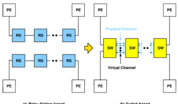
We propose a switch architecture based on the latency-insensitive concepts and utilizes the virtual-circuit switching technique to achieve high bandwidth utilization, bandwidth guarantee and predictable latency under heavy traffic condition. Relay station(RS) is used for pipeline the long interconnect in latency-insensitive design. The topology of relay station connection is shown in the Figure 2. In order to improve the low utilization of the dedicated peer-to-peer connections, the RSs are replaced by our switches and the virtual channels are substituted for the connections between RSs.
Figure 2. Transformation from relay station to switch.
B. Switch Design
The proposed switch architecture using the hybrid of virtual channel scheme, the weighted round-robin scheduling, and SRAM-based configuration is capable of providing high-throughput, bandwidth guarantee, economical memory usage, and deadlock free. We summarize the switch capabilities as follows:
First, each switch based on virtual-circuit switching owns the advantages of predictable behavior and the real-time response. The switches use the virtual channel flow control to enhance the overall latency and the throughput of a network. For example, in Figure 3, there are two messages crossing the physical channel between switches SW1 and SW2. Without using the virtual channel technique, the message data will buffered at the input or output of the physical channel. Moreover, the transfer in this channel will be blocked until the buffers are released. In this paper, the messages can be delivered rather than blocked by dividing the physical channel into several virtual channels. The waiting time of the message transfer is reduced, and the average latency of this channel is decreased. Thus, the physical channel gets higher utilization and the network obtains a larger throughput.
Figure 3. An example of virtual channel scheme.
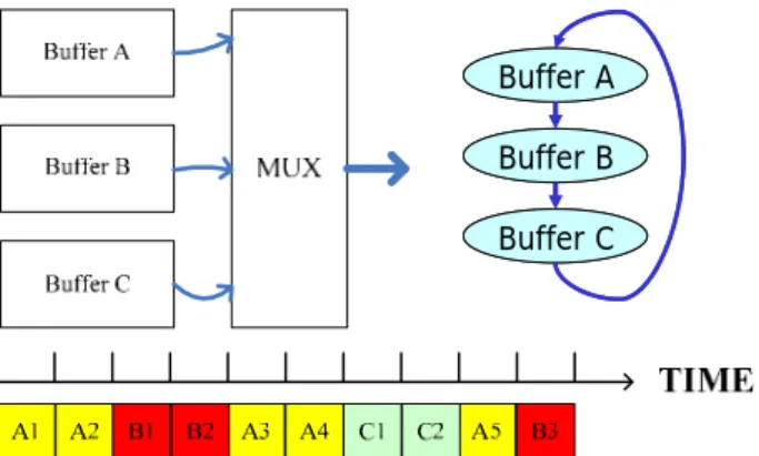
Second, concerning the bandwidth sharing of a physical channel among all the virtual channels, we exploit the weighted round-robin scheduling scheme to grant the use of the physical channel to each virtual channel. Instead of using the time-division method, the weighted round-robin scheduler as shown in Figure 4 allocates different bandwidth for each virtual channel by assigning different amount of the time slots. The higher weight of a channel means that more communication bandwidth is available. Buffer A Buffer B Buffer C Buffer A Buffer B Buffer C
Figure 4. Bandwidth allocation of a physical channel using a weighted round-robin scheduler.
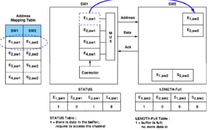
Third, the data exchange protocol between two switches or between the switch and the network interface of the local processor is executed within four clock cycles. Figure 5 shows that the interface transaction between two adjacent switches, SW1 and SW2. The address mapping table records the destination address to which the messages are transferred. At the first cycle, if the buffer, E1,sw1, of SW1 has data
inside, the system controller grants the channel priority to this data. At cycle 2, this
E1,sw1 buffer sends the address of E1,sw2 through the Address-line to indicate that this
transaction tries to deliver data to the buffer E1,sw2 of SW2. At the third clock cycle,
the buffer E1,sw2 sends the acknowledge signal, true or false, back to SW1 through
the Ack-line according to its buffer status, full or available. Meanwhile, the buffer
E1,sw1 sends the data through the Data-line, and the buffer E1,sw2 stores this data if it
has spare space. However, this data may be discarded if E1,sw2 is already full.
During the fourth cycle, the buffer E1,sw1 keeps this data until the transaction is
Figure 5. Interface transactions between two switches.
Fourth, our switch provides different memory configurations to improve the local memory utilization. The first reason is that not all buffers of the switches are reserved when the number of the connection paths is smaller than the number of the designed buffers. The second reason, the memory is a critical component for buffering data in a network. Therefore, in memory implementation, we use two-port SRAM instead of registers when the number of virtual channel is large in the physical channel. In the switch, the memory is divided into several different sizes of buffers to optimize the utilization. The memory in a switch port can be partitioned into 8 8-words blocks, 16 4-words blocks or 32 2-words blocks.
Finally, in order to support the real-time application, our switches is able to establish the dedicated connection paths in advance by reserving the corresponding virtual channels since the behavior of the communication and the number of the nodes can be predetermined in early stage of system design.
Although both the traditional circuit-switching and the proposed switching configuration have latency guarantee, our strategy not only has smaller average latency and higher hardware utilization but also has the same worse-case guarantee as compared to the worm-hole packet switching while both methods have small buffer size and high hardware utilization.
C. Quality of Service Modeling and Property
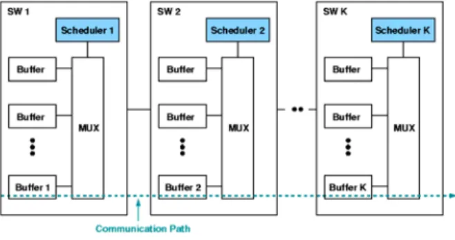
In the real-time system, the latency guarantee is the essential requirement of the quality of service (QoS) while the scheduling algorithm enables the appropriate task scheduling to satisfy the real-time requirement in the worst case condition. On the other hand, the QoS also plays a critical role even in a non-real time system. Generally, when using the communication fabric without performance guarantee, designers have to expend more design efforts to estimate the communication latency to make sure that the communication loading are not underestimated for the given on-chip network communication architecture. As a consequence, the communication system infrastructure is usually over-designed to avoid the communication congestion. In this paper, we use the weighted round-robin scheduling for our QoS model as shown in Figure 6, where the weighted round-robin scheduling is a minimal resources scheduling scheme. Each master has
a weight number Ni in the controlled scheduler. The scheduler grants the master if
the master proposes the request. The master can transmit at most Ni-word data in a
round. After that, the scheduler grants the next master until the round is complete. Our switches support to establish a predictable communication quality of NoC platform and also provide a simple communication model for reducing the design complexity. As shown in Figure 6, the communication path from Buffer 1 to Buffer
K is established. The transactions from Buffer i is granted by the weighted
round-robin Scheduler i. Before analyzing the properties of QoS model as exposed in Figure 6, the useful definitions are revealed in the following:
Figure 6. Real-time QoS modeling.
1) wi,j is the weight of the Buffer i in the weighted round-robin Scheduler j.
2) Wj is the sum of weight of the buffers controlled by the Scheduler j.
3) Dmax denotes the maximum delay of a 1-word transmission.
max burst L j max max j
4) R denotes the provided throughput rate of a buffer.
5) denotes the maximum communication path latency of a 1-word transmission.
L
6) Rpath denotes the throughput rate of a path.
7) denotes the maximum burst data latency.
Using the above definitions, the proposed network switch design has six properties to guarantee QoS, where the six QoS properties are described as follows:
Property 1: If Buffer i is empty, the maximum delay from the data arrival to the
transfer is the time period of a round in the round-robin scheduler, i.e., D =W .
Property 2: If there are data in Buffer i, the D between the transactions is W .
Property 3: If the buffer size is the double of the buffer’s weight or more, the
provided lower-bound throughput rate is the ratio of the weight and the sum of the weights in the round-robin scheduler, i.e.,
j j i W w R≥ , .
Property 4: The maximum path latency of 1-word transmission is the sum of
maximum node latency of 1-word transmission, i.e.,
∑
.= = k j j W L 1 max
Property 5: is dominated by the minimum throughput of the buffers in the path, i.e., path R } min{ , j j i path W w R = , where j=1, 2,3, …k.
Property 6: Using Property 4 and Property 5, the burst data delay can be
obtained as path burst R N L
L = max+ , where N is data size.
The Property 6 means that our switch has an upper bound of the burst data delay such that system designers can design target systems to meet real-time constraints.
The Results of Network Infrastructure
The proposed switch architecture is modeled in both cycle-accurate C++ and Verilog HDL. The C++ model is used for system design and the platform evaluation. The Verilog model is used for hardware design. After the synthesis with 0.25um standard CMOS technology, this switch can operate at 185 MHz in the typical-case corner.
In order to evaluate the traffic performance of the switch-based network platform, the C++ model of the switch is combined into the overall model of the network, and each original processing element (PE) is replaced by a random traffic pattern generator. This pattern generator generates random size packets which move from the arbitrary chosen source to the random destination.
The latency in this study means the elapsed time required for the data packet transmitted from the source node to the destination node. Maximum latency is defined as the predicted worst case latency and the maximum latency can be obtained by Property 6. Normalized latency is defined as the latency divided by the maximum latency and normalized latency indicates the average performance. Injection rate is defined as the required bandwidth of the generated traffic divided by the guarantee bandwidth of a communication path. By changing the value of the injection rate, the different communication loads are available to evaluate the platform.
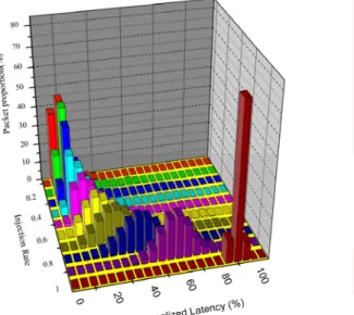
Figure 7 shows the experimental histograms of the normalized latency versus different injection rates while each virtual channel of the platform only has a 2-word buffer. The network latency guarantee (normalized latency ≦ 1) is achieved even at the high injection rate (injection rate = 1). This means that the proposed NoC platform has the property of the minimum bandwidth guarantee for each transmission. The normalized latency approaches to zero when the injection rate decreases. This indicates that the average latency reduces as the injection rate
decreases. With the property of the latency guarantee, the predictability of the proposed platform can be obtained and the real-time systems can be realized.
Figure 7. Histograms of normalized latency under different injection rate.
Figure 8 shows the normalized latency under the different buffer sizes of the virtual channels. The normalized latency reduces when the buffer size is increased. In general, the bigger buffer size of the virtual channels in the switches, the better communication performance can be achieved for the system in various applications.
Figure 8. Histograms of normalized latency under different buffer size of virtual channel. 4. 結論與討論 在本報告中,我們提出了一個適用於系統晶片的網路架構,具有高效能傳輸,保證頻 寬,可以讓系統設計者可以更加簡單的設計複雜的系統,初步的成果相當令人滿意。 表一簡列近年本研究群的相關研究成果。89 年發表會議論文 5 篇,期刊論文 6 篇,並 有 4 篇論文於IEEE期刊發表,90 年發表會議論文 10 篇,期刊論文 3 篇,並有 3 篇論文於 IEEE期刊發表,91 年發表會議論文 5 篇,期刊論文 3 篇,並於IEEE期刊發表 2 篇論文。92 年發表會議論文 12 篇,期刊論文 4 篇,並有 3 篇論文於IEEE期刊發表。93 年發表會議論
文 12 篇,期刊論文 3 篇,並有 3 篇論於IEEE期刊會議論文發表。94 年發表會議論文 11 篇, 期刊論文 1 篇,並有 1 篇論於IEEE期刊會議論文發表。 Number of Papers Domestic International Year
Conference Journal Conference Journal SCI 2000 0 0 5 6 (IEEE:4) 6 2001 2 0 8 3 (IEEE: 3) 3 2002 3 0 2 3 (IEEE:2) 3 2003 4 0 8 4 (IEEE: 3) 4 2004 3 0 9 3 (IEEE: 3) 3 2005 2 0 9 1 (IEEE:1) 1 表一、本研究群近年相關研究成果 參考文獻
[1] Liang-Yu Lin, Cheng-Yeh Wang, Pao-Jui Huang, Chih-Chieh Chou, and Jing-Yang Jou, “Communication-driven Task Binding for Multiprocessor with Latency Insensitive