國 立 交 通 大 學
電子工程學系 電子研究所碩士班
碩 士 論 文
用於 WiMax 之互補金氧半類比基頻電路設計
A CMOS Analog Baseband Design for WiMax
研 究 生:侯閎仁
Hou Hung-Jen
指導教授:溫瓌岸 博士
Dr. Kuei-Ann Wen
用於 WiMax 之互補金氧半類比基頻電路設計
學生:侯閎仁 指導教授:溫瓌岸 博士
國立交通大學電子工程學系 電子研究所碩士班
摘
要
本論文針對 WiMax 無線網路應用提出低功率高動態範圍類比基頻電路之設計。為 了達到多頻寬和高增益範圍,我們用了可單級提供 30dB 增益高範圍的假指數之 可變增益放大器(VGA)和可以改變頻寬從 0.625 MHz 到 14 MHz 的多頻寬濾波器 (LPF),在這濾波器中是由兩個轉導電路組成的元件合成的。在高動態範圍的架 構下,以較少可變增益放大器串接級來達成低功耗和用轉導電容的濾波器來減少 所需面積。最後用這 VGA 和 LPF 電路設計整個類比基頻電路並分析雜訊、線性度 和干擾。經由 0.13-μm CMOS 和 1.2 伏偏壓的製程進行電路實作,這電路可提 供 86dB 的最大功率增益、16dB 的最低增益值,並在 400mVpp 輸出電壓時約可得 40dB 全諧波失真。
ABSTRACT
This thesis presents a low-power high dynamic range design of CMOS analog
baseband circuitry for WiMax applications. To achieve multi-bandwidth and high
gain range, the proposed variable gain amplifier employs a wide-range
pseudo-exponential circuit topology providing about 30dB dynamic per-stage, and the
proposed LPF(Low Pass Filter) incorporates two adjustable transconductor achieving
various cut-off frequency from 0.625MHz to 14MHz. With the proposed topology,
the number of amplifier stages can be reduced and the level of power consumption is
tremendously lowered, and the gm-c based LPF stage help to reduce area. Base on the
proposed VGA and LPF, the topology of analog baseband is analized to consider the
trade-offs among noise, linearity and interference. The circuit is implemented in
0.13-μm CMOS process, and provides a maximum forward gain of 86 dB and a
minimum forward gain of 16 dB from a 1.2-V supply. The harmonic distortion is
誌 謝
在這碩士研究的兩年歲月,首先要感謝的是 TWT 實驗室的大家長─溫瓌岸教 授,賦予了大家豐富的資源和環境,溫文燊博士,給予精闢的教導並在研究上給 予方向,在兩位細心的指導下,完成了這篇碩士論文。另外,感謝各位口試委員 們─陳巍仁教授與詹益仁教授,提供寶貴的建議與指教。 感謝實驗室的學長姐們─、陳哲生學長、趙晧名學長、鄒文安學長、林立協 學、周美芬學姐、游振威學長、洪志德學長、賴俊憲學長、張懷仁學長與蔡彥凱 學長等在研究上的幫助與意見,讓我獲益良多。 感謝實驗室的同學─書旗、家岱、漢健、建龍、昱瑞、翔琮、義凱,在課業 和日常生活上,大家總是相互的扶持幫助;在學業上的討論與切磋。也感謝實驗 室的學弟們─柏麟、佳欣、俊彥、國爵、謙若、士賢、磊中等,讓整個實驗室充 滿了歡樂的氣息;另外,感謝 316 室的助理─怡倩、慶宏、淑怡、恩齊,時常協 助我們 最後,感謝我的每一個親人,感謝父母親在整個求學生涯的幫助,總是大力 的支持我所做的決定,感謝我的大學同學,在我有困難時都會馬上來幫我,感謝 我所有的朋友,在我心情低落時能支持我;大家在我的成長過程中,一路陪伴著 我,鼓勵我,向未來邁進。 誌予 2007 侯閎仁.A CMOS Analog Baseband Design for WiMax
摘
要
... I ABSTRACT... II 誌 謝 ...III LIST OF FIGURES...VI LIST OF TABLES...IX CHAPTER 1... 1 INTRODUCTION... 1 1.1 MOTIVATION... 1 1.2 WIMAX SYSTEM REQUIREMENTS... 3 1.3 ORGANIZATION... 6 CHAPTER 2... 7
ARCHITECTURE OF ANALOG BASEBAND... 7
2.1 TOPOLOGY ANALYSIS FOR ANALOG BASEBAND CIRCUIT... 7
2.2 TUNABLE BANDWIDTH LPF DESIGN FOR WIMAX ... 10
2.2.1 Tunable bandwidth requirements for WiMAX... 10
2.2.3 LPF simulations result ... 15
2.3 HIGH DYNAMIC RANGE VGA DESIGN... 19
2.3.1 High Dynamic Range Requirements for WiMAX... 20
2.3.2 High Dynamic Range VGA... 26
2.3.3 VGA Simulations result ... 28
2.4 TOPOLOGY PERFORMANCE ANALYSIS... 31
2.5 DESIGN OPTIMIZATION FOR NOISE FIGURE AND DISTORTION TRADEOFFS... 32
CHAPTER 3... 35
SIMULATIONS AND IMPLEMENTATION OF ANALOG BASEBAND... 35
3.1 SIMULATIONS FOR ANALOG BASEBAND CIRCUIT... 35
3.2 IMPLEMENTATION &MEASUREMENT... 42
CHAPTER 4... 49
CONCLUSION... 49
4.1 SUMMARY... 49
4.2 FUTURE WORK... 50
List of Figures
FIGURE 1 PROPOSED WIMAX TRANSCEIVER BLOCK DIAGRAM... 2
FIGURE 2 2GHZ TO 6GHZ CENTIMETER BANDS AVAILABLE FOR BWA[2]... 3
FIGURE 3 MAXIMUM ADJACENT CHANNEL INTERFERENCE C/I FOR BPSK BLOCKER PROFILE... 5
FIGURE 4 FOUR TOPOLOGIES FOR THE ANALOG BASEBAND DESIGN... 8
FIGURE 5 EXAMPLE FOR QPSK BLOCKER PROFILE... 9
FIGURE 6 A0.625MHZ PASSIVE LPF ... 11
FIGURE 7 DIFFERENTIAL GM CONNECTED AS RESISTANCE... 11
FIGURE 8 DIFFERENTIAL GM ARE CONNECTED AS INDUCTANCE BY GYRATOR APPROACH... 12
FIGURE 9 5TH ORDER GM-C LPF ... 13
FIGURE 10 SINGLE NMOS OPERATING IN TRIODE REGION... 13
FIGURE 11 PROPOSED ACTIVE CASCODE TRANSCONDUCTOR HALF CIRCUIT... 14
FIGURE 12 FULLY DIFFERENTIAL ACTIVE-CASCODE TRANSCONDUCTOR CIRCUIT AND CMFB... 15
FIGURE 13 SIMULATION RESULT OF LARGE-SIGNAL DIFFERENTIAL SMALL TRANSCONDUCTOR... 16
FIGURE 14 SIMULATION RESULT OF LARGE-SIGNAL DIFFERENTIAL BIG TRANSCONDUCTOR... 16
FIGURE 15 FREQUENCY RESPONSES OF LPF WITH SMALL GM... 17
FIGURE 16 FREQUENCY RESPONSES OF LPF WITH BIG GM... 17
FIGURE 17 HARMONIC SIMULATION OF LPF WITH SMALL GM AND 0.4VPP 200KHZ INPUT SIGNAL AND VCON=0.5V ... 18
FIGURE 18 HARMONIC SIMULATION OF LPF WITH BIG GM AND 0.4VPP 200KHZ INPUT SIGNAL AND VCON=0.55V... 18
FIGURE 19 SCHEMATIC OF THE CONVENTIONAL VARIABLE GAIN AMPLIFIER [4] ... 20
FIGURE 20 CONVENTIONAL CIRCUIT APPROXIMATION... 21
FIGURE 21 THE CONCEPT OF THE PROPOSED METHODOLOGY... 22
FIGURE 23 PROPOSED SIMULATION... 25
FIGURE 24 (A)IDEA DESCRIPTION OF HOW TO FIT PMOS PAIR AND NMOS PAIR INTO LOW VOLTAGE HEADROOM (B)THE TOTAL VGA CIRCUIT FOR RAIL-TO-RAIL TOPOLOGY... 26
FIGURE 25 SCHEMATIC OF THE VGA ... 26
FIGURE 26 COMMON MODE FEEDBACK CIRCUIT... 27
FIGURE 27 DYNAMIC GAIN RANGE SIMULATION RESULT... 28
FIGURE 28 DYNAMIC RANGE SIMULATION RESULT FOR DIFFERENT VCRL... 29
FIGURE 29 PHASE MARGIN SIMULATION FOR PMOSVGA ... 29
FIGURE 30 PHASE MARGIN SIMULATION FOR GM CELL. ... 30
FIGURE 31 THE OPTIMIZATION FOR NOISE FIGURE AND INTERFERENCE IN ONE LPF AND VGAS ANALOG BASEBAND DESIGN... 33
FIGURE 32 DYNAMIC GAIN RANGE SIMULATION RESULT IN TOPOLOGY(1)... 36
FIGURE 33 DYNAMIC GAIN RANGE SIMULATION RESULT BY HARMONIC SIMULATION IN TOPOLOGY(1) 36 FIGURE 34 FREQUENCY RESPONSES OF ANALOG BASEBAND WITH SMALL GM IN TOPOLOGY(2) ... 37
FIGURE 35 FREQUENCY RESPONSES OF ANALOG BASEBAND WITH BIG GM IN TOPOLOGY(2) ... 37
FIGURE 36 FREQUENCY RESPONSE SIMULATION RESULT AFTER ADDING BUFFERS IN TOPOLOGY(1)... 38
FIGURE 37 DYNAMIC GAIN RANGE SIMULATION RESULT IN TOPOLOGY(2)... 38
FIGURE 38 DYNAMIC GAIN RANGE SIMULATION RESULT BY HARMONIC SIMULATION IN TOPOLOGY(2) 39 FIGURE 39 DYNAMIC RANGE SIMULATION RESULT IN DIFFERENT CONTROL VOLTAGE IN TOPOLOGY(2) ... 39
FIGURE 40 OUTPUT SWING SIMULATION WITH VCR=460MV ... 40
FIGURE 41 FREQUENCY RESPONSES OF ANALOG BASEBAND WITH SMALL GM IN TOPOLOGY(2) ... 41
FIGURE 42 FREQUENCY RESPONSES OF ANALOG BASEBAND WITH BIG GM IN TOPOLOGY(2) ... 41
FIGURE 43 FREQUENCY RESPONSE SIMULATION RESULT AFTER ADDING BUFFERS IN TOPOLOGY(2)... 42
FIGURE 44 VGA BLOCK... 43
FIGURE 46 LPF CIRCUIT LAYOUT... 44
FIGURE 47 ANALOG BASEBAND CIRCUIT LAYOUT... 44
FIGURE 48 TEST SETUP... 45
FIGURE 49 MEASUREMENT RESULT OF HARMONIC DISTORTION... 46
FIGURE 50 MEASUREMENT RESULT OF HARMONIC DISTORTION... 46
FIGURE 51 -3DB FREQUENCY IN DIFFERENT CONTROL VOLTAGE FOR SMALL GM... 47
List of Tables
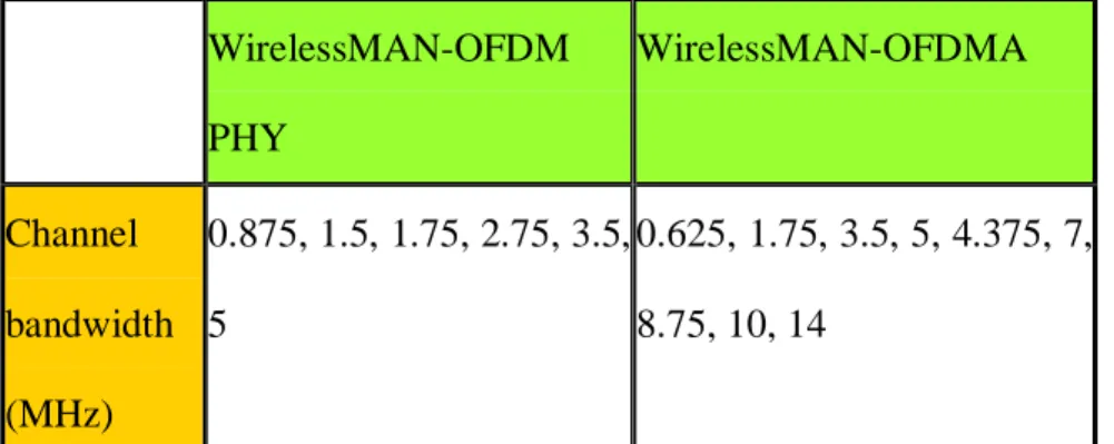
TABLE 1 CHANNEL BANDWIDTH FOR DIFFERENT PROFILES... 4
TABLE 2 THE SPECIFICATION FOR THIS ANALOG BASEBAND DESIGN... 4
TABLE 3 MINIMUM ADJACENT AND ALTERNATE ADJACENT CHANNEL INTERFERENCE PERFORMANCE AT BER 10−6... 5
TABLE 4 MINIMUM ADJACENT AND ALTERNATE ADJACENT CHANNEL INTERFERENCE PERFORMANCE AT BER 10−3... 6
TABLE 5 COMPARISON WITH NOISE FIGURE AND IN-BAND DISTORTION... 10
TABLE 6 THE SIMULATION RESULTS OF WIMAX LPF CIRCUIT... 19
TABLE 7 THE GAIN AND DYNAMIC RANGE SIMULATION RESULT IN DIFFERENT CONTROL VOLTAGE FOR A VGA ... 29
TABLE 8 THE SIMULATION RESULTS OF WIMAX VGA CIRCUIT... 30
TABLE 9THE SIMULATION RESULT OF LPF AND VGA ... 31
TABLE 10 THE GAIN AND DYNAMIC RANGE SIMULATION RESULT IN DIFFERENT CONTROL... 36
TABLE 11 THE GAIN AND DYNAMIC RANGE SIMULATION RESULT IN DIFFERENT CONTROL VOLTAGE IN TOPOLOGY(2) ... 40
TABLE 12 THE SIMULATION RESULTS OF WIMAX ANALOG BASEBAND CIRCUIT... 42
Chapter 1
Introduction
WiMAX (Worldwide interoperability for Microwave Access) is a standards-based technology defined in IEEE 802.16-2004 and IEEE 802.16e-2005. It offers the delivery of last mile wireless broadband access as an alternative to wired broadband like cable and DSL[1]. Large cover range, high transmission rate and wide variety of applications are the most obvious characteristics of this new technology, and these characteristics will cause a revolution in internet accessing of “moving” mobile device, “last mile” network constructing and even the communication network recovering after disaster. The convenience of WiMAX system not only pushes consumers to buy equipments which support the service, but saves huge money by not constructing and maintaining wires of last mile network. Therefore an enormous market can be expected, and it excites tremendous academic and industrial researches interest.
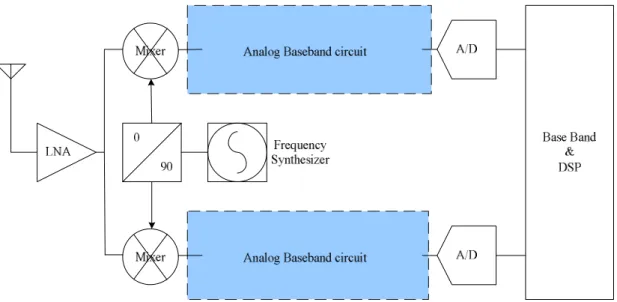
Figure 1 Proposed WiMax transceiver block diagram
For low power and low cost complementary metal-oxide semiconductor(CMOS)
process can achieve this target. The analog baseband design is between mixer and
ADC. It handles the signal that is downconverted from mixer, so the design needs low
noise and analog baseband to have high dynamic range 50dB for 10 bit ADC. The
WiMAX specification requires gain range 16~86dB and tunable cut-off frequency
from 0.625M~14MHZ. For high gain range and controlling linearly on a decibel scale,
the VGA employs pseudo-exponential circuit to generate exponential output current
for linear control signal. Nevertheless, the intrinsic device transfer characteristic of a
MOSFET is not logarithmic, and a pseudo-exponential approximation is required for
CMOS VGAs. To tune the cut-off frequency of LPF, the LPF employs
transconductor-C structure and the transconductors operate in triode region to linearty
1.2 WiMax System Requirements
Fig. 2 Shows the RF bands that can be used for WiMax. Figure shows licensed
and unlicensed band, IEEE802.16e specifies only licensed bands for mobile
application of WiMax. So the system that we design covers 2.3-2.7GHz. WiMax uses
OFDM with modulations that can be adaptively changed among BPSK, QPSK,
16QAM, and 64QAM. The channel bandwidth is 0.625M, 0.875M, 1.5M, 1.75M,
2.75M, 3.5M, 4.375M, 5M, 7M, 8.75M, 10M, 12.5M, 14M with 13channels. Table 1
shows the channel bandwidth for different profiles. So the LPF in this system requires
a tunable bandwidth technology to match the specification.
2 US WCS MVDS 3 4 5 6 2305-2320 2345-2360 2500-2690 2700-2900 3.5GHz Band 3400-3600 3300-3400 3300-3400 ISM
Low & Mid U-Nll Bands 5150-5350 Upper U-Nll/ISM Band 5725-5850 WRC 5470-5725
Initial WiMax Profiles
Future WiMax Profiles
Licensed Licensed
Unlicensed Unlicensed
Figure 2 2GHz to 6GHz centimeter bands available for BWA [2]
A simple specification for a WiMax analog baseaband design is show at Table 1
required just more than 50dB. WirelessMAN-OFDM PHY WirelessMAN-OFDMA Channel bandwidth (MHz) 0.875, 1.5, 1.75, 2.75, 3.5, 5 0.625, 1.75, 3.5, 5, 4.375, 7, 8.75, 10, 14
Table 1 Channel bandwidth for different profiles
Parameters Spec.
Technology CMOS 1.3um
Power supply 1.2V
3-dB bandwidth 0.625M~14MHz
Power consumption As small as possible
Gain range 16dB-86dB
Out swing @ THD 50dB 400mVpp
Table 2 The specification for this analog baseband design
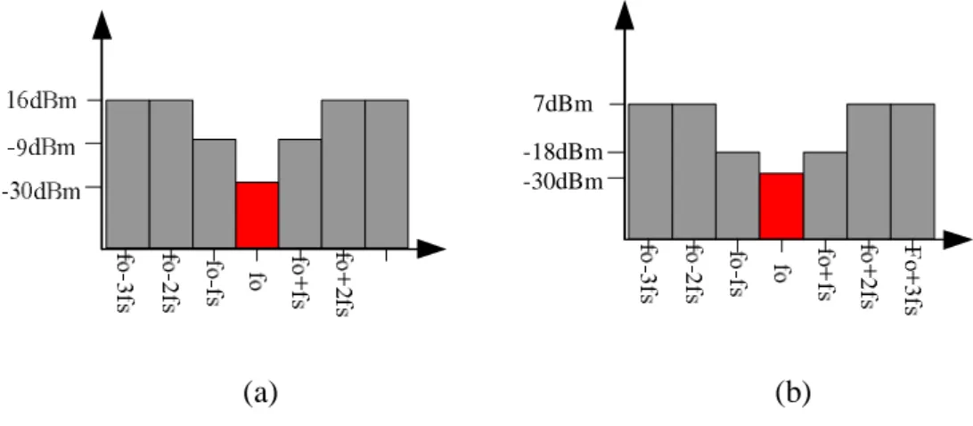
In addition, for the design considerations of adjacent and non-adjacent channel
interference, the topology of analog baseband should be carefully arrange to meet
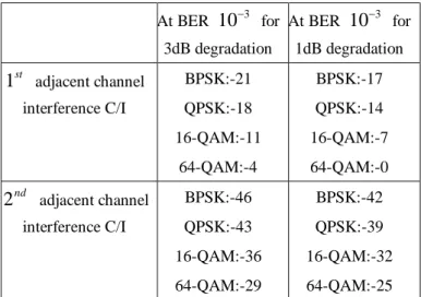
both the linearity and noise Table 1.3 is minimum adjacent and alternate adjacent
channel interference performance at BER 3
10− and 6
10− . From Table 3, Fig. 3(a) is
situation for BPSK blocker profile. The maximum input signal power is defined as in
30dBm for WiMax specification.
-18dBm 7dBm
-30dBm
(a) (b)
Figure 3 maximum adjacent channel interference C/I for BPSK blocker profile
At BER 10−6 for 3dB degradation At BER 10−6 for 1dB degradation st 1 adjacent channel interference C/I BPSK:-21 QPSK:-18 16-QAM:-11 64-QAM:-4 BPSK:-17 QPSK:-14 16-QAM:-7 64-QAM:-0 nd 2 adjacent channel interference C/I BPSK:-46 QPSK:-43 16-QAM:-36 64-QAM:-29 BPSK:-42 QPSK:-39 16-QAM:-32 64-QAM:-25
Table 3 Minimum adjacent and alternate adjacent channel interference performance
at BER 6
At BER 10−3 for 3dB degradation At BER 10−3 for 1dB degradation st 1 adjacent channel interference C/I BPSK:-21 QPSK:-18 16-QAM:-11 64-QAM:-4 BPSK:-17 QPSK:-14 16-QAM:-7 64-QAM:-0 nd 2 adjacent channel interference C/I BPSK:-46 QPSK:-43 16-QAM:-36 64-QAM:-29 BPSK:-42 QPSK:-39 16-QAM:-32 64-QAM:-25
Table 4 Minimum adjacent and alternate adjacent channel interference performance
at BER 3
10−
1.3 Organization
The organization of this thesis is overviewed as follows. Chapter 2, firstly
presents two topologies of analog baseband circuit with VGA and LPF. The design
concepts of LPF with the proposed novel tunable frequency LPF technique are
discussed. The VGA design with the novel high dynamic range VGA technique are
also presented. Finally the optimum analog baseband architecture for interference and
noise figure trade-off are analyzed. Chapter 3 describes simulation results of two
topology and LPF measurement results. Chapter 4 concludes with a summary of
Chapter 2
Architecture of Analog Baseband
In order to meet the sensitivity of WiMax and the interference requirements, the
dynamic range of adjacent channel, the analog baseband is severely affected by the
arrangement of cascading of LPF and VGA. Some condition to design the analog
baseband circuit like linearity, noise or interference. Section 2.1 discusses some
arrangements of VGAs and LPF and compare the topology arrangements in terms of
noise figure and interference. Section 2.2 discusses the design of tunable bandwidth
LPF. Section 2.3 discusses the high dynamic range VGA. Section 2.4 discusses the
optimum arrangement for interference and noise figure design trade-off.
2.1 Topology Analysis for Analog Baseband circuit
The design specification for total gain analog baseband is 16dB to 86dB.
Generally a pseudo-exponential VGA stage can achieve 30dB gain range. So it
considerations, usage of a single LPF is preferred. The Architecture includes three
VGAs and one LPF.
Figure 4 Four topologies for the analog baseband design
There are four ways to array the analog baseband as shown in Fig. 4. The design
considerations are noise figure, linearity and in-band-distortion for determining the
arrangement. ) 1 ( 1 1 2 1 1 1 ) 1 ( 1 − − + + − + − + = m p p m p tot A A NF A NF NF NF L K (2.1)
Equation (2.1) is Friis equation for cascaded stages. The gain of each VGAs is
larger than 0dB but the gain of LPF is -3dB. So arranging LPF in the first stage,
topology(1), will have the worst noise figure.
As for the linearity, each stage deals with signal with 40dB DR. The total circuit
major tone about 40dB. If LPF has better linearity, saying DR is larger than 50dB,
arranging LPF on the last stage will block the distortion produced by VGAs and the
linearity of the total analog baseband circuit depend on the LPF.
fo fo+
fs
fo
-f
s
Figure 5 Example for QPSK blocker profile
Fig. 5 is one example of signal and interference situation for QPSK blocking
profile in WiMax. When the signal comes from LNA and Mixer, adjacent channel
interference may be larger than the desired signal. It means the interference may be so
large as to make VGA into saturation without any rejection by LPF. Arranging LPF
on the first stage, topology(1) will block adjacent channel interference in advance and
avoids the VGAs getting into saturation.
From above-mentioned conditions, noise figure and interference are the trade-off.
If LPF is in the first stage, noise figure is the worst. Whereas LPF is in the last stage,
VGA may be driven into saturation. Table 5 shows the comparison of noise figure and
adjacent channel interference. The optimum arrangement depends on the practical
interference. We’ll discuss further for the optimum arrangement after the design of
LPF and VGA.
Topology(1) Topology(2) Topology(3) Topology(4) Noise Figure Bad medium Medium good
Distortion Good medium Medium bad
Table 5 Comparison with noise figure and in-band distortion
2.2 Tunable bandwidth LPF design for WiMAX
In this section, a tunable bandwidth LPF is presented. The LPF is an elliptic
fifth-order transconductor-C filter. Using transconductor-C topology can adjust
bandwidth easier without many switches and is able to reduce the capacitor. Section
2.2.1 presents the tunable bandwidth technique with transconductor-C cell. Section
2.2.2 presents the design of transconductor. Section2.2.3 presents the simulation result
of the LPF.
Figure 6 A 0.625 MHz passive LPF
Fig. 6 is a passive LPF and the cut-off frequency is 0.625M Hz. Passive LPF is a
basic topology and has the best linearity, but it needs larger area for the inductors and
capacitors. For changing the bandwidth of passive LPF, lots of devices such as
resistor and inductor have to be tuned at the same time. So designing tunable
bandwidth LPF requiresmore switches and larger chip area.
In this design we use transconductor-C topology to implement the LPF.
Transconductor can replace the resistors and inductors, hence the LPF only contains
gm blocks and capacitors. Fig. 7 and Fig. 8 show the common replacement of
resistance and inductance by Gm blocks.
1/ Gm
2
/
C Gm
Figure 8 Differential Gm are connected as inductance by gyrator approach
Tuning the bandwidth of the LPF can be done by tuning the value of the gm, and
then the bandwidth will be linear to gm. In the design, the bandwidth range of LPF is
0.625M ~ 14M Hz so the gm need to magnify 22.4 times. In order to decrease the
difficulty of signal transconductor and increase the linear range of Gm cell,therefore,
two transconductors are employed achieve the range of gm. Fig. 9 shows the
transconductor-C LPF and each transconductor block contains both large and small
transconductors. A small transconductor employ as a buffer after the LPF and
increase a little gain.
For the same inductance value, the smaller transconductor enables less
capacitance as well as small area, however, smaller transconductors are subject to
noise and process variation. Therefore the gm range of small gm is edited to l0u ~50u
3Gm + - + -Gm + - + -Figure 9 5th order gm-c LPF
2.2.2 Tunable bandwidth transconductor design
For the tunablility of gm cell, a triode-biased MOS is adopted supply a linear gm
[3]. +
-G V D I + -D G tn V <V −VFigure 10 Single NMOS operating in triode region
Fig. 10 is a NMOS operating in triode region and has high linearity between the
gate voltage and the drain current. The transconductance of the transconductor is the
D D G dI Gm gm V dV β = @ =
(
)
1 2 / 2 D ox G tn D D I =µC W L V −V V − V β is µC W Lox / for the NMOS. It can be observed the characteristic of linearity in
voltage-to-current transfer characteristic is obtained and be controlled by drain
voltage. VDD G V out I con V M1 M2 M3 M4 o I
Figure 11 Proposed active cascode transconductor half circuit
Fig. 11 is a active-cascode transconductor core. M1 is a triode-biased transistor,
its drain voltage is set by the control voltage Vcon. M2 and M3 have feedback loop to
stabilize the circuit. Current source I provides a little current which make M3 o
operate in weak inversion and M3 doesn’t share the current of M1. The gm of M1 can
be controlled and linear to the gate voltage of M3. M2 and M4 mirror the signal
current to the output. M14 and M15 are the switches to switch the small and big transconductors. Input swing is limited by Vcon and
1 1
G tn D con tn
V −V >V =V −V to
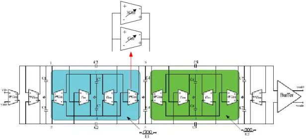
4 1 2 gm Gm gm gm = g Figure 12 Fully differential active-cascode transconductor circuit and CMFB
The transconductor is showed in the Fig. 12. M1 is the input transistor. M5 is an
active load to share the signal and increase the linear range. In the VGA design M1,
M5, M11 and M55 are four input transistors for two differential small VGA circuit.
M3 operate in weak inversion to control the drain voltage of M1 and M5. M6 is the
current source. M2, M4 and M9 are the current mirror. M9, M10 and M11 provide
negative current signals and connect to output. M12 and M13 is the current output of
CMFB circuit and connect to the drain of M8 and M9 respectively. The same gm cell
I is used a summer in the proposed of the VGA design.
0.35 con V = V 0.5 con V = V
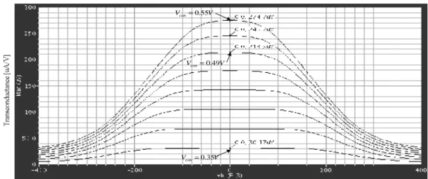
Figure 13 Simulation result of large-signal differential small transconductor
0.35 con V = V 0.55 con V = V 0.49 con V = V
Figure 14 Simulation result of large-signal differential big transconductor
Fig. 13 and 14 show the simulation results of small and big gm for large-signal
differential transconductor with 1.2V supply voltage. The range of transconductance
Figure 15 Frequency responses of LPF with small gm
Figure 16 Frequency responses of LPF with big gm
Fig. 15 is the 5th-order LPF frequency response simulation result with small transconductor and the bandwidth is 0.6147~4.175 MHz. Fig. 16 is the 5th-order LPF frequency response simulation result with small transconductor and the bandwidth is
1.925~16.65 MHz. The tunable frequency range covers the specification. The DC
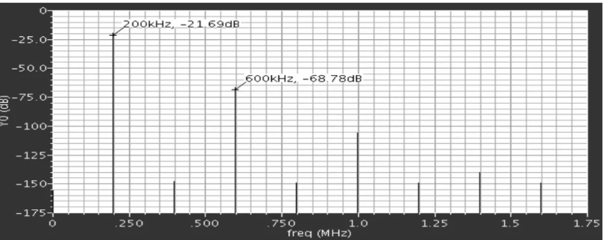
Figure 17 Harmonic simulation of LPF with small gm and 0.4Vpp 200 KHz input
signal and Vcon=0.5V
Figure 18 Harmonic simulation of LPF with big gm and 0.4Vpp 200 KHz input
signal and Vcon=0.55V
A signal with 0.4Vpp 200 KHz is input to characterize the linearity. Fig. 17 is the
LPF harmonic simulation result for Vcom=0.5 with small transconductors and the
dynamic range is 47.38 dB. Fig. 18 is the LPF harmonic simulation result for
com
V =0.55 with big transconductors and the dynamic range is 47.09 dB. The total
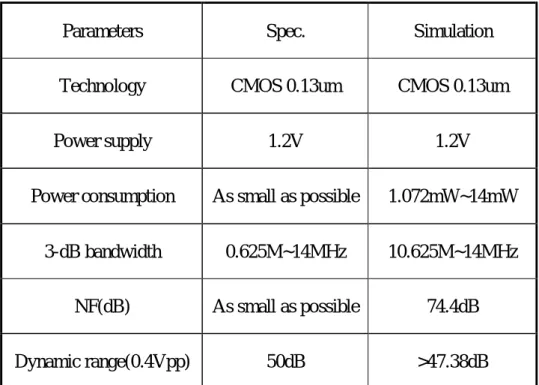
Parameters Spec. Simulation
Technology CMOS 0.13um CMOS 0.13um
Power supply 1.2V 1.2V
Power consumption As small as possible 1.072mW~14mW
3-dB bandwidth 0.625M~14MHz 10.625M~14MHz
NF(dB) As small as possible 74.4dB
Dynamic range(0.4Vpp) 50dB >47.38dB
Table 6 The simulation results of WiMax LPF circuit
Table 6 shows the summary of the LPF simulation results.
2.3 High dynamic range VGA design
The section presents the proposed variable gain amplifier (VGA) circuit for high
dynamic range applications. The gain range of VGA increases to 8.6~32dB to
compensate the non-ideal -10dB DC gain of LPF. Section 2.3.1 discusses one
example of pseudo-exponential topologies to approximate its gain polynomial to
exponential and improve the gain range. In addition, rail to rail topology is used to
increase the dynamic range. Section 2.3.2 discusses the variable gain amplifier
2.3.1 High Dynamic Range Requirements for WiMAX
A pseudo-exponential gain control using MOS transistors had been developed as
shown in Fig. 19 [4]. The amplifier make use of a source-couple pair with diode
connected load. The output is the diode connected load (1/gm) since the gain will be
equivalent to input and load transconductance ratio. The circuit consists of three part,
gain cell (M1-M8), gain control (M11-M14), and common mode feedback. The gain
cell possesses the pseudo exponential gain transfer curve with respect to the linear
gain control signal that come from gain control circuit. Common feedback is used to
stabilize the output common mode voltage.
load I in I b I ref V 2 b c I +I 2 b c I −I ctrl V
Figure 19 Schematic of the conventional variable gain amplifier [4]
transistor varied with the change of control current. The current through input and
load is constantly and equally to the current of PMOS (M7 and M8), so the output
voltage will be constantly, too. The gain control block is another PMOS source couple
pair (M11 and M12). The gain control current is a mirror to the tail current source
(M5 and M6) of input source coupled pair and load respectively. The gain is
proportional to the square root of the approximated polynomial as show in equation
below (2-1). in load gm gain gm = ( / ) ( / ) ox in in ox load load C W L I C W L I µ µ = g g ( / ) ( / ) ox in b c ox load b c C W L I I C W L I I µ µ + = − g (2-1) 1 1 x K x + = − g
Figure 20 Conventional circuit approximation
Range:
In equation (2-1), the transconductance of input and load transistor varies with
the changes of current. The gain range is limited by the square-root nature of the
device. The maximum gain range is showed in Fig. 20. In Fig. 20, the variable x is the
ratio of the additional current I to DC bias current c I when control signal is b
applied. Because the square the gain range is limited to about 15dB per stage.
The proposed approach[5] aims to improve the gain range by canceling the
square-root of equation (2-1). The proposed method is change the control current with
the varied voltage. The concept can be expressed as following:
in M Mload
x
+
V
x
−
V
x V VxFigure 21 The concept of the proposed methodology
The pseudo exponential technique is based on equation (1+x) / (1-x). If we restrict
the gate voltage of PMOS current source at the same time, we will increase (decrease)
voltage simultaneously. From Fig. 21 supplying a V and a opposite xx V increases
and decrease V and in Vload respectively. The transconductance is proportioned to
the over voltage of current source.
( / ) ( / ) in in i load load l gm W L I gain gm W L I = = (2-2)
(
)
2 M ox ctrl t W I C V V L µ = − (2-3) 1 1 x gain k x + = × − gain range 2 1 1 x x + = − (2-4)If the over-drive voltage replaces the control variable X in (2-4) then the gain
range will not be limited by square root.
in M
M
load ctrlV
+
V
V
DD ctrl shf inverter V −V −V − +VV VDD−Vctrl−Vshf DC− −VVFigure 22 Propose technique
is like reference circuit which has the same source couple gain cell but is different
from control circuit instead. An inverter is used to reverse V . And a DC-level shift x
circuit is empilied to make it to shift the circuit DC level. The ratio of input to load
transconductances is expressed as following:
( / ) ( / ) in ox in i load ox load l gm C W L I gain gm C W L I µ µ = = ( / ) ( / ) ( / ) ( / ) DD shf inverter tp ox in ox i ox load ox l DD shf DC tp V V V V C W L C W L C W L C W L V V V V µ µ µ µ − − − − + = × − − − V V (2-5)
With the condition,
Vshf inverter− =Vshf−DC (2-6) equation (2-5) is further simplified.
1 1 x gain K x + = × − where ( / ) ( / ) ( / ) ( / ) ox in ox i ox load ox l C W L C W L K C W L C W L µ µ µ µ = DD shf inverter tp DD shf DC tp V V x V V − V V V − V = = − − − − V V (2-7)
From the above description, the pseudo exponential equation (1+x) / (1-x) is
satisfied under the proposed method. The simulation result is shown in Fig. 23 and the
gain range is about 30dB. Next we will use rail-to-rail topology to increase dynamic
Figure 23 proposed simulation
With 0.13 CMOS FDK, the output swing of the proposed circuit can be
expressed as.
3
swing DD t
V =V − −V V (2-8) V
Where V is the overdrive voltage for a MOS operated in saturation region. Assume t
t
V ≈0.35, VV ≈0.2 and VDD=1.2V, the Vswing is 0.25 Vpp. The output swing is too small to match the specification that has dynamic range 50dB for 0.4 Vpp. Rail-to-rail
technique is applied to improve the output swing and the linear range. The proposed
circuit design consists of a PMOS mode VGA, a NMOS mode VGA and a low gain
OP to sum up the two path signal from rail to rail. From Fig. 24(a), when the signal
voltage is approach to ground the P devices act, while the signal voltage is close to
VDD the N devices act. The complete architecture is shown in Fig. 24(b). The low
gain OP is the gm cell and described in the section 2.2.2, and the low gain amplifier Range:
can increase the gain to meet specification. When the control voltage change, the DC
operation point will change and the output swing voltage can’t approach ideal rail-to-rail swing (VVDD gnd− ), the dynamic range is still improved at least 6dB.
I
Vin
PMOS NMOS
Figure 24 (a) Idea description of how to fit PMOS pair and NMOS pair into low
voltage headroom (b) The total VGA circuit for rail-to-rail topology
2.3.2 High Dynamic Range VGA
in M Mload ctrl V i M i M Ml Ml 1 M M1 2 M 3 M 4 M 5 M 6 M 7 M
Figure 25 Schematic of the VGA
a DC-level shift. Transistors M and i M form the gain cell. Transistorsl M and in
load
M are used to control input and load transconductance together with the control
voltage as mention earlier. Transistor M is the current source and is adjusted by 1
common-mode feedback (CMFB) to stabilize the output DC points. Transistors
2
M ~M are for the DC-level shift. Transistors 5 M and 6 M are the inverter to 7
invert the control voltage.
There is an important parameter to be taken attention. In Equation (2-7), when
the parameter K is 1, the ideal gain range is from -15dB to 15dB. Parameter K is the
ratio of input transconductance to load transconductance. Because the gain range of
specification is from 8.6dB to 32dB, the value of K can be adjust the shift gain range.
In this design the value of K is 2 and the gain of the low gain OP is increased too. In
order to reduce power consumption, transistors M , 1 M and i M is design to make l
the cut-off frequency of LPF to match the maximum cut-off frequency requirement.
Fig. 26 is the common mode feedback circuit to stabilize output. The common
feedback output V connects to cm M gate to apply a DC negative feedback. The 1
feedback loop will adjust the current source. The Output DC level is important in
multi-stage design. If the output DC level of the first stage is not stable, the following
stages will not operate at the best state and will decrease the total gain range.
2.3.3 VGA Simulations result
Fig. 27 shows the simulation result of the VGA gain range. Fig. 28 shows the
dynamic range at each control voltage.
0 5 10 15 20 25 30 35 40 0.35 0.37 0.39 0.42 0.44 0.46 0.48 0.5 0.53 0.55 0.57 0.59 0.61 Vcrl G ain Gain Figure 27 Dynamic gain range simulation result
Figure 28 Dynamic range simulation result for different Vcrl
Vcr(V) 0.35 0.372 0.394 0.416 0.438 0.46 0.482 0.504 0.526 0.548 0.57 0.592 0.614 Gain(dB) 10.34 12.71 14.92 17.04 19.11 21.17 23.21 25.26 27.31 29.3 31.2 32.95 34.48 DR(dB) 36.44 45.39 69.75 48.41 44.37 42.36 41.09 40.29 39.86 39.81 40.24 41.17 42.56
Table 7 The gain and dynamic range simulation result in different control voltage
for a VGA
The gain is not the same for each VGA requirement, it can be better linearity.
The VGA gain range simulation result is about 10.3dB~34.4dB.
Fig. 29 is PMOS VGA AC simulation result whose phase margin is 89.35deg
and is worse than NMOS VGA. Fig. 30 is gm cell AC simulation result whose phase
margin is 96.57 deg. The total VGA bandwidth is limited by low gain amplifier and
the -3dB frequency is 14.79 MHz.
Figure 30 Phase margin simulation for gm cell.
Parameters Spec. Simulation
Technology CMOS 0.13um CMOS 0.13um
Power supply 1.2V 1.2V
Power consumption As small as possible 2.184mW~4.287mW
Gain range 8.6 ~32dB 10.3dB~34.4dB
NF(dB) As small as possible 28.8dB
Dynamic range(0.4Vpp) 50dB >39.81dB
Table 8 shows the summary of the a VGA simulation results. The noise figure is
28.8dB.
2.4 Topology performance analysis
Now we can analysis the topologies by VGA and LPF from section 2.2, 2.3.
Table 9 shows the two circuit simulation results.
Block LPF VGA Bandwidth 0.615M~16.65MHz 14.79MHz Gain range -10dB 10.3dB~34.4dB NF(dB) 74.4dB 28.8dB Dynamic range(0.4Vpp) >47.38dB >39.81dB
Table 9the simulation result of LPF and VGA
We mainly analyze the noise figure and interference are analyzed to decide which topology can fit the WiMax specification and which have better performance.
From topology(1), LPF arranges in the first stage and A 5-order elliptic LPF can
reject 30dB gain at least. Since the maximum 1 adjacent channel interference C/I is st -21, so the LPF can reject the interference and no VGA stage will be saturated. But
the noise figure will be the worst. After simulation the noise figure of topology(1) is
74.4dB.
the maximum swing is -4dBm. The interference will be amplified 10.3dB to 9.3dBm
and it exceeds -4dBm (0.4Vpp) after a VGA, and the next stage, LPF, will be
saturated. At BER 3
10− the maximum interference is -13dBm which considers -3dB
attenuation in RF front end. The interference will be amplified 10dB to -3dBm.
Topology(2) is constrained to be fit the interference specification at BER 3
10− . After
simulation the noise figure of topology(2) is 51.87dB.
Only topology(1) can fit the interference requirement at BER 6
10− and
Topology(2) is constrained to fit the interference specification at BER 3
10− needless
to say topology(3) and topology(4).
2.5 Design Optimization for Noise Figure and Distortion
Tradeoffs
Topology(1) can reject interference to avoid circuit into saturation but it has bad
NF. Topology(2) has better NF but next stage, LPF, may be drove into saturation.The
gain of the first stage influences the NF and interference.
Generally a specification will specify the maximum interference that the system
can tolerate. When LPF rejectsthe interference that almost saturate LPF, the design is
Figure 31 is an analog baseband circuit that has a tunable dB-linearity gain topology
and LPF can insert in any location. The circuit can provide A~B dB gain. Each VGA and LPF has the same maximum input and output swing Vm (Vp−p) m dBv. The
maximum input signal power is define Vp ( p dBv)
Figure 31 The optimization for noise figure and interference in one LPF and VGAs
analog baseband design
Now consider the system receives maximum interference that the system can
tolerate. In this time, the signal is maximum and interference is maximum in this
worst case. So the gain of circuit will be set to minimal mode A dB. Suppose LPF
inserting in location X can filter the interference and that is the optimization. The
interference just makes the next VGA into saturation. In this situation, the interference
is amplified X dB and has m dBv swing. The adjacent channel interference C/I that
1 ( 1) 1 Y 1 X
X X
VGA LPF
tot optimum VGA
VGA VGA LPF NF NF NF NF A A A − − − = + − + + ∗ (2.9) 1 1 1 ( 1) X Y X VGA VGA tot worst LPF LPF VGA LPF NF NF NF NF A A A − − − = + − + + ∗ (2.10)
The noise figure we can improve is Equation (2.11) that Equation(2.10) subtracts
Equation(2.9). 1 1 ( ) X X X VGA LPF LPF VGA LPF VGA NF NF NF NF NF A A − − = − + − (2.11)
So we can find the optimum location for LPF with Table 3. We definite the
maximum deference of signal and interference is I. Consider the gain of LNA is 8dB
and the attenuation in channel is 3dB.
I = − −m X p
4 ( 25) 21 0( )
X = − − = − − −m p I − = dB
If the lowest gain of first VGA is 0dB, the analog baseband circuit can avoid nest
stage into saturated and have the best noise figure at BER 6
10− for WiMax
Chapter 3
Simulations and Implementation of Analog
baseband
In the chapter we show the simulation result of topology(1) and topology(2). In the latest tape-out the design uses topology(2) to arrange the VGAs and LPF even
though Case(s) can’t satisfy the worst interference specification but it almost can fit
the specification at BER 3
10− . The difference between topology(1) and topology(2) is
only the position of LPF, so the frequency response and harmonic simulation result
will be almost the same. Section 3.1 presents the simulation result of our analog
baseband circuit. Sec 3.2 presents the implementation and the measurement result of
LPF.
3.1 Simulations for Analog baseband circuit
The last tape-out topology(2) is chosen, but we show the simulation result of two topologies. The VGAs and LPF design have been described in chapter 2.2 and
section.
Figure 32 Dynamic gain range simulation result in topology(1)
0 10 20 30 40 50 60 0.34 0.36 0.38 0.41 0.43 0.45 0.47 0.49 0.51 0.53 0.55 0.57 0.59 0.62 Vtrl D yn am ic r ange DR
Figure 33 Dynamic gain range simulation result by harmonic simulation in
topology(1)
Vcr(V) 0.34 0.36 0.38 0.41 0.42.5 0.45 0.47 0.49 0.51 0.53 0.55 0.57 0.59 0.62 Gain(dB) 15.24 21.88 27.3 33.8 39.66 45.45 51.21 56.97 62.73 68.43 74.19 79.25 84.01 88.35
DR(dB) 30.98 38.66 51.82 50.15 50.15 43.42 39.34 38.38 38.5 38.32 38.17 39.73 40.89 42.07
Table 10 The gain and dynamic range simulation result in different control
33 shows the dynamic range simulation result in different control voltage and the
output swing is 0.4Vpp. The dynamic range of analog baseband circuit is less than
VGA about 2dB.
Figure 34 Frequency responses of analog baseband with small gm in topology(2)
Figure 35 Frequency responses of analog baseband with large gm in topology(2)
Fig. 34 and 35 show the frequency response simulation result with small and big
respectively. From Fig. 35 we can see the -3dB gain frequency have degraded to
about 2MHz. This is because there is a parasitic pole between LPF and VGA. The pole equation is parasitic 1
LPF LPF VGA
Pole
R C +
=
LPF
R is the output resistor and CLPF VGA+ is the sum of parasitic capacitor of LPF and
VGA. So the gain degraded before frequency bandwidth expected.
Figure 36 Frequency response simulation result after adding buffers in topology(1)
A buffers is added between LPF and VGA and simulation again. Fig. 36 shows
the simulation result and the maximum -3dB frequency is 5.3MHz. The -3dB
frequency can’t increase to 14MHz is because the VGA -3dB frequency is 14.79MHz.
The gain of VGA drops before 14MHz. After accumulating two VGA blocks the
analog baseaband circuit -3dB frequency will decrease to 5.3MHz.
0 20 40 60 80 100 0.35 0.37 0.39 0.42 0.44 0.46 0.48 0.5 0.53 0.55 0.57 0.59 0.61 Vcrl G ain Gain
Figure 38 Dynamic gain range simulation result by harmonic simulation in
topology(2) 0 10 20 30 40 50 60 70 0.35 0.37 0.39 0.42 0.44 0.46 0.48 0.5 0.53 0.55 0.57 0.59 0.61 Vtrl D yn am ic r ange DR
Figure 39 Dynamic range simulation result in different control voltage in
topology(2)
Vcr(V) 0.35 0.372 0.394 0.416 0.438 0.46 0.482 0.504 0.526 0.548 0.57 0.592 0.614 Gain(dB) 15.44 22.4 28.78 34.9 41.06 47.09 53.14 58.58 65.18 71.03 76.62 81.69 86.69 DR(dB) 31.43 42.61 61.71 45.52 42.03 40.52 38.76 39.72 37.62 38.19 38.36 39.92 41.74
Table 11 The gain and dynamic range simulation result in different control voltage
in topology(2)
Figure 40 Output swing simulation with Vcr=460mV
Fig. 37 shows the gain range ac frequency response and Fig. 38 shows the gain
range for harmonic simulation with output swing 0.4Vpp in topology(2). Fig. 39
shows the dynamic range simulation result in different control voltage and the output
swing is 0.4Vpp too. The transient simulation is shown in Fig. 40. Under the
trl
V =460mV the output swing is 0.4Vpp for differential output with 40dB dynamic
Figure 41 Frequency responses of analog baseband with small gm in topology(2)
Figure 42 Frequency responses of analog baseband with large gm in topology(2)
Fig. 41 and 42 show the frequency response simulation result with small and
large gm cell in LPF respectively. From Fig. 41 the -3dB gain frequency has degraded
about 2.7MHz. Topology(2) has the same problem of topology(1). Fig. 43 shows the
Figure 43 Frequency response simulation result after adding buffers in topology(2)
Parameters Spec. Topology(1) Topology(2)
Technology CMOS 0.13um CMOS 0.13um CMOS 0.13um
Power supply 1.2V 1.2V 1.2V
3-dB bandwidth 0.625M~14MHz 0.625B~5.3MHz 0.625B~5.3MHz
Power consumption As small as
possible 7.624mW~26.8mW 7.624mW~26.8mW NF As small as possible 84.9dB 51.87dB Gain range 16dB-86dB 16~86dB 16~86dB Dynamic range(0.4Vpp) 50dB >38.17dB (0.4Vpp) >38.19dB (0.4Vpp) Table 12 The simulation results of WiMax analog baseband circuit
3.2 Implementation & Measurement
Fig. 44 shows the layout of VGA block and the size is 120um x 79um. There are
Figure 44 VGA block
The layouts of two Gm block is shown in Fig. 45(a) and Fig. 45(b). Small Gm
and large Gm are only different from MOS size and the layout is close small to reduce
parasitic capacitance. The size of small Gm is 21um x 22um. The size of large Gm is
24um x 22um.
(a) Small Gm block (2) Big Gm block3
(a) LPF block
Figure 46 LPF circuit layout
(a) Layout of Topology(1) (a) Layout of Topology(2)
Figure 47 Analog baseband circuit layout
The layout of LPF block is shown in Fig. 46. The size of LPF is 463.1um x
273.6um. The layout of analog baseband circuit layout of topology(2) is shown in Fig.
47(b). In order to reduce area, a switch is added before buffer to switch the first VGA
output or total circuit output to characterize the output signal of VGA. The layout of
Figure 48 Test setup
Fig. 48 is the testing setup for measuring chip on wafer. In the circuit spectrum
analyzer is used to measure frequency response and dynamic range. All of the design
are fully-different. A transformer is applied to convert signal after ESG and before
Spectrum analyzer.
Fig. 49 show a measurement result of harmonic distortion of the LPF when small
Gm is opened and Vcrl=0.4. Because transformer has -8dB loss, 4dBm signal from
ESG and LPF receives -4dBm signal for 0.4Vpp. From measurements the pole and
zero is shifted the simulation but we can see the LPF still have two zeros. Fig. 50
shows the harmonic distortion measurement result when input signal is 4dBm at
-60 -50 -40 -30 -20 -10 0 0. 51 1. 48 2. 51 3. 01 3. 51 4. 01 4.5 4. 99 6. 01 7. 02 8. 03 8. 97 10 11 12 13 14 MHz dB
Figure 49 Measurement result of harmonic distortion
Figure 50 Measurement result of harmonic distortion
Several chip samples were measured and recode the -3dB from flat gain in
respectively. The -3dB frequency is linearity to the control voltage. Because of the
parasitic capacitor and the variation of gm cell, the -3dB bandwidth of different chips
don’t match the simulation results.
Figure 51 -3dB frequency in different control voltage for small Gm
Figure 52 -3dB frequency in different control voltage for big Gm
Parameters Spec. Topology(1) Topology(2) APMC.2005[6]
Technology CMOS0 .13um CMOS 0.13um CMOS 0.13um CMOS 0.16
Standard WiMax WiMax WiMax WLAN
Power supply 1.2V 1.2V 1.2V 1.8V 3-dB bandwidth 0.625M~14MHz 0.625B~6.2MHz 0.625B~5.3MHz 7.56 19.5 26.5MHz Power consumption As small as possible 7.624mW~26.8mW 7.624mW~26.8mW 22.248mW NF As small as possible 84.9dB (734.2uV/sqrt(Hz)@output noise) 51.87dB (42.19uV/sqrt(Hz)@output noise) Gain range 16dB-86dB 16~86dB 16~86dB 20~60dB Dynamic range 50dB (0.4Vpp) >38.17dB (0.4Vpp) >38.19dB (0.4Vpp)
Parameters APMC.2005[7] JSSC.2006[8] TCSI.2006[9]
Technology CMOS0.13um CMOS0.18um CMOS0.13
Standard UMTS WLAN WLAN WLAN UMTS Power supply 2.5V 1.6-2V 1.2 3-dB bandwidth 3.4~40MHz 2.1,11MHz Power consumption 55mW 11.6mW 19.44mW NF 51uVrms(IRN) 77.5nV/squrHz(Input noise) 1.12mVrms(output noise) Gain range -6~68dB -8-32dB 8dB
Dynamic range 1.4%@ -8dB gain 52(1.4Vpp)
Chapter 4
Conclusion
The thesis has presented an analog baseband circuit employing a linear-in dB
VGA and a tunable LPF for WiMax. It includes of three 14MHz low power VGA and
a tunable bandwidth low power LPF. The novel topology has been applied to the
analog front-end for WiMax direct conversion receiver which perform low power,
wide dynamic gain range and high data rate. In conclusion, the key contributions
presented in previous chapters are summarized below.
4.1 Summary
An optimum arrangement of LPF and VGA for noise figure and interference
trade-off is presented. Two transconductor operating in triode region for a tunable
transconductor-C LPF is presented. A linear-in dB topology employing novel pseudo
exponential technique for a low power VGA is presented. We use three VGA blocks
implemented in 0.13-µ m CMOS process and arrange LPF in second location. The
circuit provides a minimum gain of 16dB and maximum gain of 86dB while drawing
26.8wW from a 1.2-V supply. The dynamic range is 38.19dB for 0.4Vpp. The
measurement result of LPF is presented
4.2 Future Work
In the thesis, there are some design considerations which we didn’t attention. We
give some recommendations and improvement in the section. First the analog
baseband design is not optimum. The 2nd and 3rd VGA block gain range can be changed to have larger output swing for total design. The loading of each block didn’t
consider comprehensively so the bandwidth was limited. Second the non-ideal resistor
of each transconductor is considered too much so the pole and zero will shift from the
ideal value and the frequency response will decrease in advance. The layout didn’t
consider parasitic capacitors completely. Third the control circuit of the VGA block is
only an inverter and DC shift circuit and the better choice is use OP to do control
circuit. We didn’t consider best choice is using OP for control circuit. We will make
an improvement in the future work.
Bibliography
[1] IEEE 802.16-2004 document.
[2] Farahani, B.J.; Ismail, M.; “WiMAX/WLAN radio receiver architecture for convergence in WMANS”;Circuits and Systems, 2005. 48th Midwest Symposium on7-10 Aug. 2005 Page(s):1621 - 1624 Vol. 2
[3] Yodprasit, U.; Enz, C.C. “A 1.5-V 75-dB dynamic range third-order G/sub m/-C filter integrated in a 0.18-/spl mu/m” JSSC.2003.
[4] Po-Chiun Huang; Li-Yu Chiou; Chorng-Kuang Wang “A 3.3-V CMOS wideband exponential control variable-gain-amplifier;” ISCAS.1998.704417
[5] Chao-Chun Sung, Mei-Fen Chou and Kuei-Ann Wen, "Low Power CMOS Wideband Variable Gain Amplifier", Proc. IASTED Int. Conf. on Circuits, Signals, and Systems, Clearwater Beach, Florida, U.S.A., pp. 126-129, (November 2004).
[6] Kai-Yin Liu; Chun-Hao Chen; Yu-Che Yang; Hsiao-Chin Chen; Shih-An Yu; Shey-Shi Lu; ”A low power fully integrated analog baseband circuit with variable bandwidth for 802.11 a/b/g WLAN” Digital Object Identifier 10.1109/APMC.2005.1606465
baseband channel for GSM/UMTS/WLAN/Bluetooth reconfigurable multistandard terminals” Digital Object Identifier 10.1109/ISCAS.2006.1693580
[8] Ghittori, N.; Vigna, A.; Malcovati, P.; D'Amico, S.; Baschirotto, A.;”A 1.2- V 30.4-dBm OIP3 Reconfigurable Analog Baseband Channel for UMTS/WLAN Transmitters” Digital Object Identifier 10.1109/TCSI.2006.883174
[9] Jeon, O.; Fox, R.M.; Myers, B.”A.; Analog AGC Circuitry for a CMOS WLAN Receiver”/JSSC.2006.881548
![Figure 2 2GHz to 6GHz centimeter bands available for BWA [2]](https://thumb-ap.123doks.com/thumbv2/9libinfo/8611875.190788/13.892.154.735.553.1012/figure-ghz-ghz-centimeter-bands-available-bwa.webp)