振動式環形微陀螺儀接合製程
64
0
0
全文
(2) 振動式環形微陀螺儀接合製程 Bonding Process for the Vibrating Ring Gyro 研 究 生:鄭斌佐. Student:Pin-Tso Cheng. 指導教授:成維華. Advisor:Wei-Hua Chieng. 國 立 交 通 大 學 機械工程研究所 碩 士 論 文. A Thesis Submitted to Institute of Mechanical Engineering College of Engineering National Chiao Tung University in partial Fulfillment of the Requirements for the Degree of Master of Science In. Mechanical Engineering June 2004 Hsinchu, Taiwan, Republic of China. 中華民國九十三年六月.
(3) 振動式環型微陀螺儀接合製程. 研究生:鄭斌佐. 指導老師:成維華 教授. 國立交通大學機械工程研究所. 摘要 由於陽極接合(anodic bonding)可以在低溫(<500℃)下將玻璃與 矽接合且有很可靠的接合強度,所以相當普遍地用在製造微感測器。 陽極接合也用在我們的振動式環形陀螺儀的製造上。但是我們遭遇到 非接合區域有些黏結在玻璃上的問題。我們粗糙化非接合區域來改善 非接合區域黏結在玻璃上的情形。一開始在深蝕刻過程中我們是用厚 膜光阻當作遮罩,但是光阻再流動非常嚴重。這將會影響結構的溝口 (gap) 的寬度和深度我們利用二氧化矽取代厚膜光阻當作蝕刻阻擋層 成功地解決了光阻再流動的問題。 關鍵字:陽極接合、深蝕刻、光阻再流動. i.
(4) Bonding Process for the Vibrating Ring Gyro. Student: Pin-Tso Cheng. Advisor: Dr. Wei-Hua Chieng. Institute of Mechanical Engineering National Chiao Tung University. Abstract Anodic bonding is a quite popular process used in fabricating micro sensors since it is a glass-to-silicon bonding process with reliable bonding strength in lower temperature (<500℃). It is applied in the fabrication of our vibrating ring gyro, but we suffered the problem that the part of non-bonding region was bonded to glass. We rough the non-bonding region to reduce the situation that non-bonding region was boned to glass. Initially, we used the thick photoresist (PR) as DRIE process mask, but the photoresist reflow is very serious. It will influence the width and the depth of the structural gap. We use SiO2 instead of thick PR as DRIE etching mask and successfully solve the PR reflow problem. Keyword: anodic bonding, DRIE, photoresist reflow. ii.
(5) Acknowledgments I would like to express my deep sense of appreciation to my advisor, Dr. Wei-Hua Chieng, for his outstanding guidance and earnest inspiration during my graduate study and research. I thank my family and my friends. Their concern and support is significant to me everyplace. Finally, I thank people and Precision Instrument Development Center (PIDC) that favor my study and research.. iii.
(6) Contents 摘要…………………………………………….………………………..i Abstract……………………………………….………………….……ii Acknowledgement……………………………………………………iii Contents………………………………………….…………...…….…iv Table List……..………………………………………..……………...vi Figure List……………………………………………………………vii Chapter 1 Introduction………………....….…………….....……….….P. 1 1.1 Introduction………………..…..........…….…..…....……..…..P. 1 1.2 Related Researches .......…………………....…….............…..P. 2 1.3 Motivation ..…………………………..........................…..…..P. 3 Chapter 2 Principles of Bonding Techniques….................…………….P. 5 2.1 Introduction……… ………..………................…………..…..P. 5 2.2 Wafer direct Bonding ..…………….............……………..…..P. 5 2.2.1 Background of WDB………………....................…..…….P. 5 2.2.2 Mechanism of Wafer Direct Bonding…..…...….………....P. 6 2.3 Anodic bonding…….….………….......................………..…..P. 9 2.3.1 Background…………..…………….…….…......…………P. 9 2.3.2 Bonding Mechanism……………….…….…...…..………P.10 2.3.3 Bonding Strength of Anodic Bonding.…………………P.12 2.3.4 Process Variations.……………………..……..…..………P.12 Chapter 3 Fabrication Technology…………………….……...…….P.14 3.1 Introduction………………..……………….…………….…P.14 3.2 Surface Cleaning….……………..………………….………..P.14 3.3 Deposit SiO2 with PECVD …………......................……..P.15 3.4 Deposit Aluminum with Thermal Evaporation Coater…P.16 3.5 Photolithography process… ………………………….……..P.16 3.5.1 Primer Coating process………….….…………….……P.16 3.5.2 Photoresist Coating……....…………….………………P.17 3.5.3 Soft Bake……………………………………………….P.18 3.5.4 Exposure……..……............................………………....P.18 3.5.5 Development……………………..………………………P.19 3.5.6 Hard Bake……………..……………..…..………………P.19 iii.
(7) 3.6 Etch Aluminum and SiO2 with HDP-RIE…………….….P.20 3.7 Fabricate the Microstructure with ICP-RIE……............…..P.20 3.8 Generate the Bonding Field…………………………....…..P.21 3.9 Dry Oxidation…………………………………..……….....P.22 3.10 Anodic Bonding………………………..……….…………..P.23 3.11 Etch Back with TMAH………………………....…………P.24 3.12 Remove the Protective Layer of SiO2…………...………..P.25 Chapter 4 Fabrication Results and Discussion…..................................P.26 Chapter 5 Conclusions and Suggestions for Feature Works …………….………………………………………...................P.30 Reference……………………………………………………….……P.31. iv.
(8) Table List Table 2-1 The parameters of the deposited SiO2 with PECVD ……P.36 Table 2-2 The parameters of etching aluminum and SiO 2 with HDP-RIE ……………………………………………………………P.37 Table 4-1 The parameters of roughing non-bonding region……...…P.38. v.
(9) Figure List Fig. 1.1 The profile of micro gyro structure.(unit: µm)………..…..….P.39 Fig. 2.1 Schematic of wafer-bonding process flow................................P.40 Fig. 2.2 Schematic of tree types of interactions between two solids………………….…….....................................................P.41 Fig. 2.3 Borosilicate glass with space charge region at the silicon glass interface during anodic bonding……….................................P.42 Fig. 2.4 Bond strength vs. SiO2 thickness………….......….……….…P.42 Fig. 3.1 The original fabrication flow chart........................................P.43 Fig. 3.2 The phenomenon of photoresist reflow..................................P.44 Fig. 3.3 The modified fabrication flow chart……...................……....P.45 Fig. 3.4 After etching aluminum process………………….…..............P.46 Fig. 3.5 The SiO2 mask………………....................................………..P.46 Fig. 3.6 The bonding fields after dry etching process…….............….P.47 Fig. 3.7 The profile of silicon after dry oxidation…….......………….P.48 Fig. 3.8 Etch rate of (100) silicon as a function of TMAH concentration and temperature……………………………………....……....P.49 Fig. 3.9 etch rate of SiO2 as a function of TMAH concentration and temperature…………………………….............……………P.49 Fig. 4.1 The dummy field was bonded to glass……….....…………..P.50 Fig. 4.2 The defect of lithographic process………………....……….P.50 Fig. 4.3 The surface before roughing process……………........…….P.51 Fig. 4.4 The surface after roughing process…………………......…P.52 Fig. 4.5 The profile of the SiO2 mask…………………….................P.53. vi.
(10) Fig. 4.6 The profile after dry etching process………........……….…P.53 Fig. 4.7 The real cross-section after dry etching process, the bottorn of the trench is closed………………...…………………....……….P.54 Fig. 4.8 The vibrating ring……………......……………………...…....P.54. vii.
(11) Chapter 1 Introduction. 1.1 Introduction Within the last few years “wafer bonding” techniques have become important as a basic technology for microelectronics and micromechanics. Wafer bonding is a key element in the fabrication of micromechanical devices. The bonding the techniques allow the stacking of complex 3-D structures for micro sensors and actuators in a very economical and precise manner [1]. There are a number of different methods available for bonding micromachined silicon wafers together, or to other substrates, to form more complex devices. The two dominant wafer bonding techniques are anodic bonding and wafer direct bonding. In the following section, the applications of wafer bonding will be discussed. Micro gyroscopes have found large attention in recent years due to their low-cost, small-size, and some unique features making them ideal for several commercial and military applications, e.g. inertial navigation, control system, defense, avionics and space. Due to the rapid development of semiconductor technology, the micro electromechanical system. (MEMS). including. the. micro-machined. gyroscope. and. accelerometer follows the trend of the modern sensor requirement. The various fabrication technologies, structural designs and drive/sense. 1.
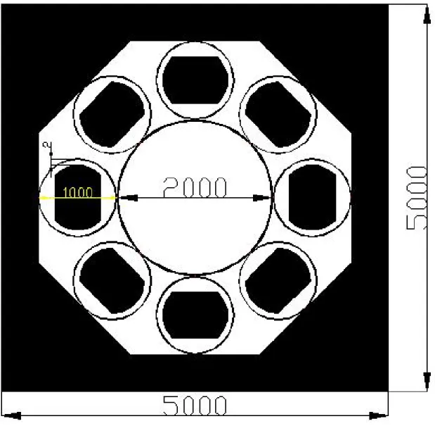
(12) mechanisms for micro-gyroscopes have been investigated. Our vibrating ring gyroscope which is shown in Fig. 1.1 consists of the main ring, eight support rings, and eight electrodes. The main structure of vibration ring gyro made by deep reactive ion etching (DRIE) of a silicon substrate is bonded to PYREX 7740 glass by anodic bonding.. 1.2 Related Researches The typical applications of bonding techniques are to integrated pressure sensors and fabricate accelerometer. The integrated silicon pressure sensors reported here are fabricated using standard IC processes to establish the electronic circuitry on the frontside of a silicon wafer. Subsequently, small cavities are formed on the backside by an anisotropic etching process that employs an electrochemical etch stop. A thin membrane is thus created on each die of the wafer. A differential pressure applied across the membrane will produce a mechanical stress within the membrane, which is transformed into an electrical signal by integrated piezoresistors. The silicon chip incorporates the entire signal conditioning and circuitry for electronic trimming [4,5]. The accelerometer described in the following is a capacitive discrete sensor. It consists of three layers. All wafers are fabricated separately by anisotropic etching techniques. The middle plate of the sensor chip bears the moveable seismic mass, which is fixed with a beam. Upper and lower plates are the counter 2.
(13) electrodes. The three wafers are electrically isolated by SiO2-layers and are bonded together by bonding techniques [28]. A method of bonding silicon to glass that appears to be gaining in popularity is anodic bonding (electrostatic bonding). The first application in silicon micromachining were reported more than 20 years ago [6]. The silicon wafer and glass substrate are brought together and heated to a high temperature. A large electric field is applied across the join, which causes an extremely strong bond to form between the two materials. It is also possible to bond silicon wafers directly together using wafer direct bonding. Other bonding methods include using an adhesive layer, such as a glass, or photoresist. WDB is an attractive technology for VLSI, semiconductor power and sensor device applications. WDB processes are applied to fuse bare or oxidized silicon wafers to each other [29]. The method of WDB was first published in 1986 [30].. 1.3 Motivation In our fabrication process, We use anodic bonding to join silicon and glass substrates. There are two mainly benefits of anodic bonding: (1) anodic bonding (300 ℃ ~500 ℃ ) is a low temperature process compared to WDB (800℃~1200℃) [23]. (2) Due to the electrostatic attraction, anodic bonding shows a better step. 3.
(14) coverage. Particles have less influence on the bonding process than in the case of WDB[23]. In initial process, we use the photoresist (AZ-P4620) to resist etching. But The photoresist reflow was serious during the dry etching process. So we utilize the SiO2 as mask to resist dry etching. The method successfully solves the problems caused by the thick photoresist.. 4.
(15) Chapter 2 Principles of Bonding Techniques 2.1 Introduction The two major bonding techniques (WDB and AB) have been used to fabricate micro-electro-mechanical structures (MEMS) for variety of sensors and actuators. In the following sections, the principles of the two bonding techniques will be discussed respectively.. 2.2 Wafer Direct Bonding 2.2.1 Background of WDB The expression “wafer direct bonding” refers to the phenomenon that mirror-polished flat and cleaned wafers of almost any material, when brought into contact at room temperature, are locally attracted to each other by Van der Waals forces and adhered or “bonded” to each other. Wafer direct bonding generally refers to a process by which two mirror-polished wafers adhere to each other at room temperature without the application of any macroscopic gluing layer or outside force. After starting the bonding process by locally applying a slight pressure to adjacent wafers [7]. Therefore, for many applications, the room temperature bonded wafers have to undergo a heat treatment to strength the bonds across the interface. Frequently one of the two wafers is then thinned to a thickness that depends on the specific application and may be 5.
(16) in the range of many microns down to a couple of nanometers. Although by no mean required, in most cases the wafers involved in actual applications. are. typical. semiconductor. wafers. consisting. of. single-crystalline material used in micro- or optoelectronics such as silicon or gallium arsenide. This is the concept of the activation method.. 2.2.2 Mechanism of WDB There are mainly three types of surface forces acting between two solid in sufficient proximity: (1) Van der Waals attraction forces, (2) electrostatic Coulombic forces, and (3) capillary force. It is well known that electrically polarized or at least polarizable (identical or different) atoms or molecules are attracted to each other by so-called Van der Waals interaction. Van der Walls forces originate from atomic and molecular electric dipoles whose orientations are correlated in such a way that they attract each other. Usually one distinguishes between the following three types of Van der Waals forces: (1) the dipole-dipole force between two polar molecules, (2) the dipole-induced force between a polar and a nonpolar molecules, and (3) the dispersion force between two nonpolar molecules resulting form the nonzero average value of the square of the temporary dipole moment due to charge distribution fluctuations [8, 9]. It should be noted that in some disciplines the term “Van der Waals force” refers only to the dispersion force. The three Van der Waals forces are all 6.
(17) considered being long ranged on an atomic scale, but short ranged on a macroscopic scale. The hydrogen bond is not a strong bond compared to covalent bonds (e.g., the bond energies of 1.9 and 4.5 eV for a Si-Si bond and a Si-O bond, respectively). However, the hydrogen bond can play a key role in reactions. occurring. at. normal. temperature,. such. as. that. in. room-temperature wafer bonding, owing to its relatively weak bond and the small activation energy involved in its formation and rupture. If hydrogen bonding can be realized across two mating surfaces, it will result in strong dipole-dipole Van der Waals attraction forces between these surfaces. Moreover, when the mating surfaces are hydrophilic and water molecules are present, the linkages of two or three water molecules may bridge the gaps between the two mating surfaces. Since the size of an OH group is 1.01Å [10] and the distance between two hydrogenbonded oxygen atoms in ice is 2.76 Å [11], hydrophilic Si surface separated up to 10 Å can be bridged to adhere through clusters of three hydrogen bonded wafer molecules at room temperature. [12] (see Fig. 2.1 [7]) This long-range hydrogen bonding will cause the smoothness requirements of the mating surfaces for successful room-temperature bonding. The purpose of surface activation is thus to realize a reactive surface with practically available smoothness and flatness for room-temperature bonding. 7.
(18) As discussed above, silicon wafers with hydrophilic surfaces can bond to each other at room temperature. This has been attributed to the pressure of OH groups on the mating surfaces that form hydrogen bonds between the two wafers. It has been found that hydropholic Si wafers prepared by a dip in diluted HF without subsequent water rinse show a similar room temperature-bonding performance [13]. When the DI water rinse is not performed after a dilute HF dip, the Si surfaces are mainly terminated by H, but a significant amount of F, about 0.12 of a monolayer [14] or ≦1×10¹⁴ atoms/cm2 [15], has also been found on the silicon surface. The bondability of the HF-dipped Si wafers is most likely correlated to the presence of Si-F bonds. Recently, thermal-adsorption spectroscopy results [16, 17] show some physisorbed HF residual molecules on the Si surface after HF dip without a DI water rinse. The distance between two fluorine atoms of F-H … F in a hydrogen-bonded polymer H-F … H-F … H-F is 2.55Å [18]. The bond angle in the gas polymers is reported to be ~140° [18]. Crystal chemistry has shown that F ions and OH ions are similar. Not only are they of approximately the same size, but they are also isoelectric [19]. It is therefore conceivable that, similar to the hydrophilic wafer bonding via hydrogen-bonded water linkages, a cluster of three or more hydrogen-bonded HF molecules may bridge the two mating surfaces so that two surfaces which are separated 8.
(19) up to 8Å can still be bonded by hydrogen bonding (see Fig. 2.2 [7]). It should be noted that in order to avoid the roughening of the Si surface during an HF dip, very diluted HF aqueous solutions such as 0.6~1% HF have to be used for a short time ranging from 15sec to 5 min at room temperature. After hydrophilic surface formation, Water molecules come out and the voids (intrinsic) are observed beyond 200℃. The voids tend to disappear and bonding strength is increased at more than 300℃ forming siloxane (Si-O) bonds. At high temperatures (>800℃), Oxygen at the interface may diffuse into the silicon bulk to form Si-Si bonds like single crystal silicon at above 1000℃.. 2.3 Anodic Bonding 2.3.1 Background Anodic bonding [20] has become a key process in microsensor and microactuator technology within the last 15 years. Other commonly used for this technique are Field Assisted Bonding or Electrostatic Bonding. The process is often used for joining silicon with glass at temperatures below the softening temperature of the glass [21]. However this technique can also be used for joining metals or alloys with glass or ceramics provided that the surfaces of the materials to be bonded are polished, very 9.
(20) plane and free of particles and that the thermal expansion coefficients of the two materials are closely matched[20],[22]. The equipment for the process consists of a hot plate on which the parts to be bonded are heated to temperatures between ca. 300℃ and 500 ℃ and a DC-power supply which is connected in such a way to the two parts that the silicon is positively charged with respect to the glass, it is shown in Fig. 2.3.[23]. 2.3.2 Bonding Mechanism Usually borosilicate glass (PYREX 7740 glass) is used which have thermal expansion coefficients that almost equal the thermal expansion coefficient of silicon and which have the necessary electrical conductivity at the temperature at which the bonding process occurs PYREX 7740 glasses consist of approximately 80% SiO2, 13% B2O3, 3.5% Na2O, and 2.35% Fe2O3, Al2O3. A necessary requirement for a good seal is that the two parts have a very intimate physical contact. For anodic bonding this is achieved by applying the DC-voltage mentioned above across the two parts. Without applying an external force the mirrorlike bond partners are separated by a gap of several μm. The applied voltage (400V-1000V) creates an electrostatic field in the gap which generates an electrostatic force that pulls the parts into intimate contact. At the same time Na+ ions. 10.
(21) which are mobile at the bonding temperature move through the electrostatic field from the glass/silicon interface to the negative electrode where they are neutralized. This causes a depletion of free positive ions in the region near the glass/silicon interface. The fixed negative ions remaining create a space charge region (Fig. 2.3[23]). The bonding chemistry is yet not thoroughly understood. It is assumed that due to the high electric field oxygen ions leave the glass and create Si-O-Si bonds, i.e., a thin SiO2 layer is formed. This assumption is strengthened by the fact that the bonding process is irreversible. In addition, the formation of a thin SiO2 layer was verified by RBS (Rutherford Backscattering) [24]. The progress of the bonding process can be observed optically or by measuring the current through the silicon-glass-stack or by measuring the space charge capacitance. Contact for the electrical voltage is generally made between the heating plate (anode) beneath the silicon and a point contact (cathode) on the glass. The bonding process starts at the point contact and spreads radially. The radial spreading of the bonding front makes it impossible for air to become trapped between the silicon and the glass. To avoid contamination of the bonding areas by particles the bonding process has to be performed in a clean room of class 100 or better. However, it is possible to bond around small particles because of the electrostatic attraction of the bond partners. 11.
(22) 2.3.3 Bond Strength of Anodic Bonding To determine the bond strength several methods, e.g., pressure test, pull test, shear test, and bending test and are used. Due to the different ways the force is applied different values for the bond strength are obtained from each method for samples bonded with the same process parameters. To determine the influence of the process parameters on the bond strength the same test method has to be used for all experiments. From our experiments it was not possible to determine the real bond strength, i.e., the strength with which the silicon and the glass are bonded to each other, since the break in all samples occurred in the glass and not at the silicon/glass interface. In values for the bond strength between 30 MPa and 40 MPa were determined from pull tests[23].. 2.3.4 Process Variations It is not only possible to join one silicon part with one glass part by anodic bonding but also to fabricate multi wafer stacks of several bond partners made of silicon and glass. E. Obermeier has successfully fabricated three-layer (silicon/SiO2/glass) structures. Fig. 2.4 [23] shows the measured values for the bond strength for thermally oxidized silicon vs. the thickness of the oxide. The figure shows that with oxidized silicon almost the same bond strength can be obtained as with bare silicon. 12.
(23) However, with increasing oxide thickness the process time increases dramatically. Our SiO2 thickness is about 150~200 nm and the bond strength is about 30 MPa from Fig. 2.4 [23].. 13.
(24) Chapter 3. Fabrication Technology. 3.1 Introduction The initial fabrication process flow is shown in Fig. 3.1 [25]. The phenomenon of photoresist (AZ-P4620) reflow is very serious. The phenomenon will influence the real size of the gap after dry etching process. The phenomenon of photoresist reflow is shown in Fig.3.2 [25]. We use SiO2 layer instead of photoresist as mask to resist dry etching to avoid the photoresist reflow. The modified fabrication process flow is shown in Fig. 3.3.. 3.2 Surface Cleaning Microstructure requires wafers with clean surfaces which are free of particulate, organic, and metallic contaminations. Clean and flat wafer surface is important because the surface conditions have a direct effect on both the structural and electrical properties of the bonding interface as well as on the resulting electrical properties of the bonded materials. The first step in the RCA Clean is preliminary cleaning. We use a mixture of H2SO4: H2O2 (3:1 by volume) to remove organic film. Wafers are immersed in the solution at 85℃-100℃ for about 10 minutes. Then the wafers are rinsed in de-ionized (DI) water for 5 minute. The next step is SC-1, it is mainly removing organic films, certain metals, and particles. It 14.
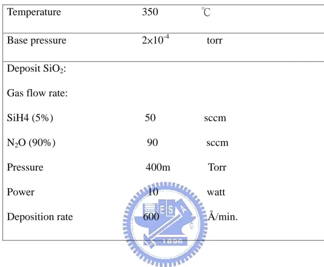
(25) is a mixture of H2O: H2O2: NH4OH (5:1:0.25 by volume) heated to 75℃. The wafers and their holder are submerged in the solution for 10 minutes. The wafers are then rinsed in DI water for 5 minutes. The third step is SC-2, which can remove the Alkali and heavy metals. It is a fresh mixture of H2O: HCl: H2O2 (6:1:1 by volume) heated to 75℃. The wafers are submerged in the solution for 10minutes. The wafers are then rinsed in DI water for 5 minutes. The wafers are finally rinsed in the mixture of H2O: HF (100:1 by volume) . The wafers are dried in heated N2.. 3.3 Deposit SiO2 with PECVD Plasma enhanced chemical-vapor deposition (PECVD) has the advantage of deposition thick oxide in a clean processing vicinity a at very low temperature. Its operational pressure is about 400m Torr. The film deposition is operated in a gas flow consisting of silane and N2O.Tthe PECVD oxide is not a pure silicon dioxide SiO2, it always has a small amount of hydrogen in the deposited film.. SiH 4 + N 2O. plasma → SiOx H y +H 2O+ N 2 + NH3+... heat. (reaction3.1)[26]. In plasma, electrons dissociate both silane and nitrous oxide via dissociation collisions.. e− + SiH → e− + SiH + H 4 2 2 − − e + N O → e +O + N 2 2. (reaction3.2)[26]. 15.
(26) Deposition rate is high and mainly depends on the gas flow rate. N2O is overflowed; therefore, the deposition rate is controlled mainly by the silane flow rate. The process parameters of the deposition system are listed in table 3.1. We utilize PECVD to deposit about 2μm of SiO2. The SiO2 layer is covered silicon surface as a mask to resist dry etching.. 3.4 Deposit Aluminum with Thermal Evaporation Coater Aluminum has a relatively low melting point(660℃) and boiling point(2519℃), so it is relatively easy to vaporize aluminum under low pressure. We use the system to vaporize aluminum layer (the thickness is about 5000Å). The system needs to be under high vacuum, about 10-6Torr, and the rate is about 10Å/sec. The layer of aluminum serves as the mask throughout the process sequence and transfer the pattern from photoresist to aluminum using dry etching.. 3.5 Photolithography process 3.5.1 Primer coating process The photolithography process includes three major steps: photoresist coating, exposure, and developing. Particles on the wafer surface can 16.
(27) cause pinholes in the photoresist; the organic and inorganic contamination may cause photoresist adhesion problems and device and circuit defects. Wafer clean is very important, using solvents and acids to remove organic and inorganic contaminant residues. It is a deposition process called priming. In this process a thin layer of primer, which can “wet” the wafer surface and promote adhesion between the organic photoresist and the inorganic silicon or silicon compound wafer surface, is coated on the wafer surface before the photoresist coating. Hexamethyldislazane (HMDS, (CH3)3SiNHSi (CH3)3) is the most commonly used primer in the photolithography process. The wafer is placed in YES oven (Vacuum Oven), the HMDS is vaporized, introduced into the oven chamber ,and deposited on the wafer surface. The temperature is constantly 150℃ in the chamber.. 3.5.2 Photoresist Coating photoresist coating is a deposition process in which a thin layer of photoresist is applied on the wafer surface. A positive photoresist, FH-6400L, is used in our work. Our patterned feature of main structure is shown in Fig. 1.1. We use. 17.
(28) the photo exposure system is Karl-Suss MJB-3, it is the contact printer. The highest resolution a contact printer can achieve is about 2μm. Our minimum line spacing is 2μm, so we could pattern feature which we want. The photoresist material is FH-6400L. . The spin coating includes two steps. The first step is at low spin rate, around 1000rpm. The PR will be applied at the center of the wafer. After the PR dispensed, the second step is accelerated to high spin rate, up to 4500 rpm, to spread the photoresist uniformly across the wafer surface. The thotoresist thickness is about 1μm.. 3.5.3 Soft Bake After the photoresist coating, the wafer is placed on a hot plate which temperature is 90℃ to drive out the majority of solvent inside the PR and transform the photoresist from the liquid state to solid state. This soft bake also improves the photoresist adhesion to the wafer surface. We put the wafers on the hot plate for 1 minute.. 3.5.4 Exposure Exposure is the most critical steps of the photolithography process.. 18.
(29) The patterned image on the mask is exposed to the photoresist on the wafer. We use Karl-Suss MJB-3 which is in NFC to expose our patterned image for 30 seconds. The dose is calculated as follows:. dose(. mJ mW )=intensity( ) × time(sec) cm2 cm2. (reaction. 3.3) 3.5.5 Development There are three steps in the development process: develop, rinse, and dry. The development process removes the unwanted photoresist and forms the desired pattern defined by the mask. We use FHD-5 to develop our wafers for 45 sec. but there are so many particles to cause the defects after the dry etching process.. 3.5.6 Hard Bake After development, wafers are put on the hot plate which temperature is 120℃ for 3 minutes. Hard bake drives out the remaining solvents in the PR, strengthens the PR, and improves the PR etch and implantation resistance via further thermal polymerization, and also improves its adhesion to the wafer due to further thermal dehydration.. 19.
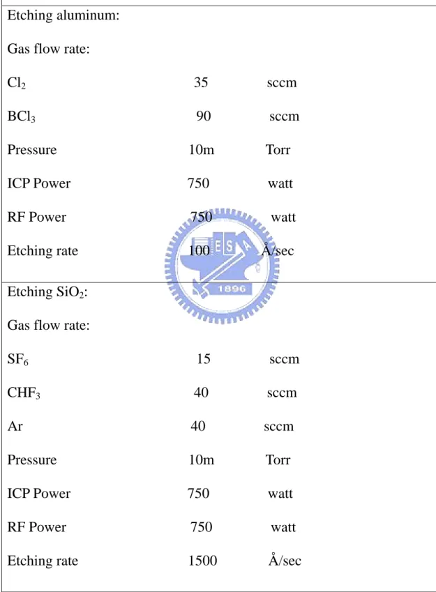
(30) 3.6 Etch Aluminum and SiO2 with HDP-RIE High-density plasma (HDP) reactors are increasingly used in dry etching in place of conventional reactive ion etching (RIE) reactors. We utilize HDP-RIE to etch aluminum. Fig. 3.4 shows the surface profile after etching aluminum process. The etchants are Cl2 and BCl3. Metal etch normally uses Cl2 as the main etchant, and BCl3 is commonly used for the sidewall passivation.. Cl. 2. plasma → Cl + Cl. plasma Cl + Al → AlCl. (reaction 2.3) 3. After aluminum etch process, we used gases for SiO2 etches are CHF3, SF6 and Ar. We fabricate the SiO2 mask to resist silicon etch process with ICP-RIE (see Fig. 3.5). Finally, we remove aluminum with a mixture of H3PO4: CH3COOH: HNO3:H2O=80: 5:5:10. The recipes of etching aluminum and SiO2 with HDP-RIE are shown in Table 2.3.. 3.7. Fabricate the Microstructure with ICP-RIE. ICP-RIE is usually used to make HARMS (High Aspect Ratio Micro 20.
(31) Structure). We utilized ICP-RIE to etch silicon to depths about 180μm. The advanced silicon etch process is based on the technique invented by Larmer and Schip, the sidewall passivation layer is necessary for an anisotropic etching deposited in a separate step from the silicon etch process. By sequentially alternating etch and deposition steps, anisotropic etching an carried out on feature sizes ranging from submicro to several millimeter in size. SF6 and C4F8 are used as the etching and deposition gas recipes. The SF6 gas supplies fluorine radicals for spontaneous isotropic etching of exposed silicon as illustrated:. CF +e- → CF + +CF * +F* +eX X 4 → CF nCF * → nCF X 2(ads) 2(f) SF +e- → S F + +S F * +F* +eX Y X Y 6 nCF +F* → CF CF X(g) 2(f) X(ads) Si+F* → Si-nF Si-nF → SiF X(ads) SiF → SiF 4(g) X(ads). 3.8. (reaction2.3). Generate the Bonding Field. We use HDP-RIE to etch the step, which avoids the ring bonding to 21.
(32) 7740 glass. First, we deposit a layer of aluminum that will serve as the mask throughout the process sequence and transfer the pattern from photoresist (FH-6400) to aluminum using Cl2 and BCl3 etching. After to transfer the pattern, aluminum is in order to serve a mask to protect the bulk silicon substrate, because the selectivity between aluminum and silicon is very high. Then we utilize SF6, CHF3, and Ar gas to etch silicon substrate, Fig.3.6 shows the bonding fields after the dry etching process. The depth of the step is about 15μm. Finally, we remove aluminum with a mixture of H3PO4: CH3COOH: HNO3:H2O=80: 5:5:10.. 3.9 Dry Oxidation. We use the frame to grow the dry oxide, the motive of the dry oxide is protecting the ring against TMAH etching. Dry oxidation has a lower grower growth rate than wet oxidation, it is a advantage for my process. Thermally grown silicon dioxide is an amorphous material. It is unstable, and the molecules tend to cross-link to form a crystalline structure. This is the main reason silicon dioxide exists in the form of quartz and quartz sand in nature. However, the crystallization process can be dramatically accelerated at the high temperature (>1000℃) required during silicon dioxide growth. If the silicon surface is not free of. 22.
(33) contamination, defects and particles can serve as nucleation sites for crystallization during the oxidation process, and silicon dioxide will grow in a polycrystalline structure like icecrystal flowers formed on glass in winter. Proper pre-oxidation wafer clean becomes very important to eliminate to eliminate the crystallization by removing the particles, organic and inorganic contaminants, native oxide, and surface defects. Wet clean process is shown in section 2.1. The gap of the microstructure is 2μm and the deep is 180μm, it is very high aspect ratio, so the property of silicon dioxide on the sidewall is very important. The thickness of the silicon dioxide is about 2000Å. Fig. 3.7 (a) shows the profile of silicon after dry oxidation, Fig. 3.7 (b) shows the bottorn of a trench. From the above figure, the sidewall is perfectly covered a SiO2 layer.. 3.10 Anodic Bonding. Anodic bonding is one of the key technologies in the fabrication and packaging of microsensors and microactuators. The difficulty in obtaining good bonds when there are intermediate layers such as silicon dioxide over the silicon wafer is well known. Fig 2.4[23] shows tensile bonding strength of silicon with different thickness of silicon dioxide bonded to PYREX by anodic bonding. Our thickness of silicon dioxide is about 2000Å, from Fig. 2.4 [23], the bonding strength is about 30 MPa. 23.
(34) 3.11 Etch Back with TMAH. TMAH water solution has started to be gradually introduced in industry and lab. This is because TMAH water solution is hardly to attack silicon dioxide which used as an etching mask. And it doesn’t have the harmful ion K that might attack the circuit on the microstructure. The etching rate of silicon is function of temperature, concentration and silicon orientation. But it is important when the concentration is lower than 25%, the etching rate decreased as the concentration decreased. U. Schnakeubery and O. Tabata developed a new organic solution, tetramethyl ammonium hydroxide(TMAH, (CH 3 ) 4 NOH ) for anisotropic etchant of silicon. The important of this etchant are non-flammable, non-toxic, less harmful for metal and CMOS compatible. The silicon etching rate of TMAH is orientation dependent. The etching rate of TMAH is very slow at [111] orientation. The etching rate is fast at[110] orientation. The etching rate ratio of [100]/[111] in TMAH is about half that KOH. So the TMAH is not suitable to fabricating structure which is the orientation [111] to be mask. The etching rate for TMAH and KOH solutions compare the orientation. Two differences were observed in the etching-rate distribution patterns of the two solution. (1)the valley of the distribution pattern around the [111] orientation for TMAH is stepper and 24.
(35) narrower than that for KOH. (2)the distribution pattern showed a plateau region starting from [110] toward [100] in the case of KOH, but it didn’t for the TMAH, but show a local minimum at [110] unlike KOH. The dependences of (100) silicon and silicon oxide etch rates in TMAH on concentration and temperature are shown in Fig. 3.8 and Fig. 3.9, respectively [27]. We use the solvent that the temperature is about 90 ℃ to etch silicon, the etch rate is about 75 μm/h. The etch rate to SiO2. is about 168 Ǻ/h.. 3.12. Remove the Protective Layer of SiO2. After wet etching process, the protective layer of silicon dioxide is not removed. We will utilize BOE to etch the layer of silicon dioxide, and simultaneously the dummy field will be fell. BOE is commonly used for the silicon dioxide wet etch. BOE solution is about 6:1 (NH4F: HF) because only HF and H2O (1:1) etches oxide too fast at room temperature. Normally, HF is further diluted either in water or in a buffer solution such as ammonium fluoride (NH4F) to slow down the oxide etch rate to control the etch rate and uniformity.. 25.
(36) Chapter 4 Fabrication Results and Discussion The main fabricated processes are discussed in the followings: (1). In the fabrication of SiO2 mask, we must deposit aluminum layer about 5000Å. The layer of aluminum serves as the mask throughout the process sequence and transfer the pattern from photoresist to aluminum using dry etching.. (2). After the above process, we utilize DRIE to fabricate the height of the rings of micro-gyroscope.. (3). During the DRIE process, the sidewall will be covered a polymeric layer caused by the C4F8 plasma. We tried using HNO3 to remove the layer, the solution has successfully removed the polymeric layer.. (4). We deposit aluminum layer about 5000 Å again, the step is to fabricate the electrode mask. The second dry etching to generate the step between the silicon and glass substrate. The step between the silicon and glass substrate is about 15 µm.. (5). The step is to oxidize silicon wafer, the SiO2 thickness is about 2000Å, then we use anodic bonding join the wafer and glass substrate.. (6). Etching backside silicon with TMAH.. During ICP-RIE etching process, the C4F8 plasma deposits a (CxFy)n polymeric passivation layer on all substrate surface. The directional ion. 26.
(37) energy supplied by the capacitively coupled platen electrode during the etch step preferentially removes the passivation layer from the bottom of the trench hence exposing silicon for spontaneous etching.. But the. passivation layer of the sidewall of the trench didn’t be removed. The layer will influence the following oxide growth process. We tried utilizing the solution HF : H2O2 with 1:1 to remove the passivation layer, but the result is bad. The layer doesn’t be all removed. Finally, we use KNO3 to remove the layer, and the result is very perfect. Dummy fields is used to avoid the phenomenon of RIE lag, it lets all the critical dimension be 2μm. Form the Fig. 1.1, the minimum line width of the gap is 2 μm, and there is a hole with radius 1 mm beside the gap. After removing the protective layer, the dummy field should be all fell. But the fact is that the dummy field is not fell, there are two probable reasons: (1). The dummy field is bonded to PYREX 7740 glass: during anodic bonding process, the electrostatic force is very strong to bond the dummy field. The distance is about 15μm between the dummy field and PYREX 7740 glass. The electrostatic force makes the microstructure deform and the. 27.
(38) deflection is larger than 15μm. Fig. 4.1 shows the dummy field boned on glass. (2). Particles influence the effect of lithography: particles will generate such as the effect of mask. It will seriously influences the following process, e.g. dry etching, wet etching, as show in Fig. 4.2.. In the first problem, we enhance the roughness of the non-bonding region; table 4.1 lists the parameters of roughing non-bonding region. Fig. 4.3 shows the surface before roughing process. The value of surface roughness (Ra) of the non-bonding region is smaller than 50 Å. After the roughing process , the non-bonding region has a measured Ra value of 693 Å (with Dektak II A). The non-bonding region without roughing process is shown in Fig. 4.4(a). Fig. 4.4(b) shows the surface of non-bonding region after the roughing process. and the other is increasing the time of the wafer in BOE (about 6 hours). We use HDP-RIE to rough the non-bond surface with CHF3 and Ar for five minutes. The Ra is about 693Å. After the above process, it is reduced that the phenomenon of dummy field bonded to glass. It is about 180 µm that the desired depth of micro-structure, but the real depth is about 120µm. The cause is that the sidewall of the SiO2 mask is not vertical, which is shown in Fig. 4.5. The problem would 28.
(39) influence the following dry etching process, Fig. 4.6 shows the profile after dry etching process. Because the amount of SF6 influences the profile of the SiO2 mask, we will try changing the recipe of the amount of SF6 during etching SiO2 mask process. Fig. 4.7 shows the real crosssection after dry etching process, the bottorn of the trench is closed. The structure is vibrating when we charge one of the eight electrodes, as shown in Fig. 4.8, the charged voltage is about 60V.. 29.
(40) Chapter 5. Conclusions and Suggestions for Feature Works. Two major contributions are carried out in this paper. First, the thick photoresist (AZ-P4620) cause the phenomenon of reflow during the drying pocess. it influences the size of the structural gap during the dry etching process. We utilize the SiO2 as mask to resist dry etching, and the method successfully solves the problem of photoresist reflow. In the fabrication of SiO2 mask, we must deposit aluminum layer about 5000Å. The layer of aluminum serves as the mask throughout the process sequence and transfer the pattern from photoresist to aluminum using dry etching. Second, the method of roughing the dummy fields is implemented. The method like gaseous chemical etchants, gas flow rate, power, process cycle time are discussed. After that, we understand that enchanced roughness of dummy fields reduces the phenomenon of non-bonding fields bonded to glass. Finally, we have the several suggestions for our fabricated processes: (1) Optimize the parameters of enhanced roughness, including gas flow rate, power, process cycle time. The step will reduce the bond strength of non-bonding region. (2) Change the parameters of dry etching process to fabricate SiO2 mask, we will try to reduce the value of SF6 and increase the time for etching SiO2. The bad SiO2 mask will influence the depth of trenches. The method will be used to achieve the desired depth of trenches. 30.
(41) References [1] K. E. Petersen, in Proceedings of the IEEE, 70, p.420(1982). [2] P. Greiff. B. Boxenhorn. T. King, L. Niles, “Silicon Monolithic Micromechanical Gyroscope,” Transducers’91, San Francisco, CA, USA; 24-27 June 1991, pp.966-8. [3] M. W. Putty and K. Najafi, “A micromachined vibrating ring gyroscope,” Digest ,Solid-State Sensors and Actuators Workshop, Hilton Head, SC, June 1994, pp. 213-220. [4] H. J. Kress, F. Bantien, J. Marek and M. Willmann, Sensors and Actuators A, 25-27, 21(1991). [5] H. J. Kress, J. Marek, M. Mast, O. Schatz, and J. Muchow, “Integrated silicon pressure sensor for automotive application with electronic trimming,” SAE Technical Paper Series 950533(1995). [6] A. D. Kurz, J. R. Mallon and H. Bernsten, ISA ASI 73246, p. 229, (1973) [7] Q-Y.TONG, and U.GOSELE, “SEMICONDUCTOR WAFER BONDING: SCIENCE AND TECHNOLOGY”, JOHN WILEY & SONS, INC, 1999. [8] C.Kittel, Introduction to Solid State Physics, 2nd ed, Wiley, New York,. 31.
(42) pp. 60, 1986. [9] R. G. Horn, “Surface Forces and their action in ceramic materials,” J. Am. Ceram. Soc., Vol. 73, pp. 1117, 1990. [10] L. Pauling, The Nature of the Chemical Bond, 3rd., Comell University Press, Ithaca, NY, pp. 468, 1960. [11] L. Pauling, The Nature of the Chemical Bond, 3rd., Comell University Press, Ithaca, NY, pp. 452, 1960. [12] T. A. Michalske and E. R. Fuller, “Closure and repropagation of healed cracks in silicate glass,” J. Am. Ceram. Soc., Vol. 68, pp. 586, 1985. [13] K. Ljungberg, A. Soderbarg and Y. Backlund, “Spontaneous bonding of hydrophobic silicon surfaces,” Appl. Phys. Lett., Vol. 62, pp. 1362, 1993. [14] T. Sunada, T. Yasaka, M. Takakura, T. Sugiyama, S. Miyazaki, and M. Hirose, “The role of fluorine termination in the chemical stability of HF-trested Si surfaces,” Jpn. J. Appl. Phys., Vol. 29, L2408, 1990. [15] D. Graf, M. Grundner , and R. Schulz, “Reaction of water with hydrofluoric acid treated silicon (111) and (100) surfaces,” J. Vac. Technol., A7, pp. 808, 1989.. 32.
(43) [16] M. Hirose, T. Yasaka, K. Kanda, M. Takakura, and S. Miyazaki, “Behavior of hydrogen and fluorine bonds on chemically cleaned silicon surfaces,” in J. Ruzyllo and R. Novak (Eds.), Proceesings of the. International. semiconductor. Symposium. Device. on. Cleaning. Manufacturing,. Technology. Vol.. 92-12,. in The. Electrochemical Society, Pennington, NJ, pp. 1, 1992. [17] G. J. Pietsch, U. Kohler, and M. Henzler, “Chemical status and surface topography of Si (111) after HF/NH4F/H2O wet chemical treatments: Investigations with STM, AES and TDS,” Materials Research Society Spring Meeting 1993, Y12.4, San Francisco, pp.459, 1993. [18] L. Pauling, The Nature of the Chemical Bond, 3rd ed., Cornell University Press, Ithaca, NY, pp. 461, 1960. [19] T. Thomas, H. Elemer, I. D. Chapman and M. E. Nordberg, “Changes in infrared transmittance of fluorine-containing porous glass on heating,” J. Chem. Phys., Vol. 62, pp. 2219, 1963. [20] G. Wallis and D. I. Pomerantz, J. Appl. Phys., 40, 1946, 1969. [21] W. H. Ko, J. T. Suminto, and G. J. Yeh, in Micromachining and Micropackaging of Transducers, C. D. Fung, P. W. Cheung, W. H.. 33.
(44) and D. G. Fleming, Editors, Amsterdam: Elsevier Science Publishers B. V., 1985 [22] K. Gustafsson, B. Hők, S. Johansson, and T. Murray, Sensors and Materials, 2, 65, 1988. [23] E. Obermeier, “Anodic wafer bonding,” Proceedings of 3th International Symposium on Semiconductor Wafer Bonding: Science and Technology and Applications, Vol. 95-7, The Electrochemical Society, Pennington, NJ, p.212,1995. [24] A. Cozma and B. Puers, Micro Mechanics Europe (MME) Workshop Digest, p.40, 1994. [25] C. Y. Tsai, “Micro vibrating ring gyroscope fabricated with fusion bonding,” pp. 40, 2003. [26] H. Xiao, “Introduction to semiconductor manufacturing technology,” Prentice-Hall Inc., 2001. [27] O. Tabata, R. Asahi, H. Funabashi, K. Shimaoka, and S. Sugiyama, “Anisotropic etching of silicon in TMAH solutions,” Sens. and Actuators A, 34, 51, 1992. [28] H. Baumann, S. Mack, and H. Münzel, “Bonding of structured wafers,”. Proceedings. of. 3th. 34. International. Symposium. on.
(45) Semiconductor Wafer Bonding: Science and Technology and Applications, Vol. 95-7, The Electrochemical Society, Pennington, NJ, p.212,1995. [29] K. Petersen, P. Barth, J. Poydock, J. Brown, J. Mallon Jr. and J. Bryzek, in Proceedings of the IEEE Soild-State Sensor and Actuator Workshop, IEEE, 144 (1988). [30] J. B. Lasky, Appl. Phys. Lett., 48, 78(1986).. 35.
(46) Table 3.1 The parameters of the deposited SiO2 with PECVD.. ℃. Temperature. 350. Base pressure. 2×10⁻⁴. torr. SiH4 (5%). 50. sccm. N2O (90%). 90. sccm. Pressure. 400m. Torr. Power. 10. watt. Deposit SiO2: Gas flow rate:. Deposition rate. 600. Å/min.. 36.
(47) Table 3.2 The parameters of etching aluminum and SiO2 with HDP-RIE. 23. ℃. Cl2. 35. sccm. BCl3. 90. sccm. Temperature Etching aluminum: Gas flow rate:. Pressure. 10m. Torr. ICP Power. 750. watt. RF Power. 750. watt. Etching rate. 100. Å/sec. Etching SiO2: Gas flow rate: SF6. 15. sccm. CHF3. 40. sccm. Ar. 40. sccm. Pressure. 10m. Torr. ICP Power. 750. watt. RF Power. 750. watt. Etching rate. 1500. Å/sec. 37.
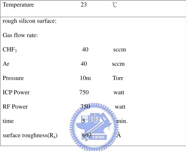
(48) Table 4.1 the parameters of roughing non-bonding region. 23. ℃. CHF3. 40. sccm. Ar. 40. sccm. Pressure. 10m. Torr. ICP Power. 750. watt. RF Power. 750. watt. time. 5. min.. surface roughness(Ra). 693. Å. Temperature rough silicon surface: Gas flow rate:. 38.
(49) Fig. 1.1 The profile of micro gyro structure.(unit: µm). 39.
(50) Surface preparation and cleaning. Room temperature bonding. Annealing. Bonding interface. Fig. 2.1 Schematic of wafer-bonding process flow. [7]. 40.
(51) Fig. 2.2 Schematic of tree types of interactions between two solids.[7]. 41.
(52) Fig. 2.3 Borosilicate glass with space charge region at the silicon glass interface during anodic bonding.[23]. Fig. 2.4 Bond strength vs. SiO2 thickness.[23]. 42.
(53) Etching electrode pattern Si. PR. Pattern Structure. Si. ICP-RIE. Oxidation SiO2. Fusion Bonding. One Side Si Etching. Released Structure. Fig. 3.1 The original fabrication flow chart. [25]. 43.
(54) Fig. 3.2 The phenomenon of photoresist reflow. [25]. 44.
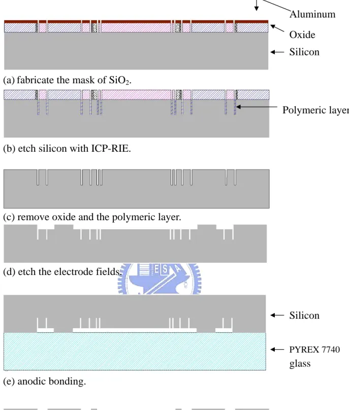
(55) Aluminum Oxide Silicon (a) fabricate the mask of SiO2. Polymeric layer. (b) etch silicon with ICP-RIE.. (c) remove oxide and the polymeric layer.. (d) etch the electrode fields.. Silicon PYREX 7740. glass (e) anodic bonding.. (f) etch back with TMAH. Fig. 3.3 The modified fabrication flow chart.. 45.
(56) Fig. 3.4 After etching aluminum process.. Fig. 3.5 The SiO2 mask. .. 46.
(57) Bonding field. Fig. 3.6 The bonding fields after dry etching process.. 47.
(58) SiO2. (a) cross-section of the microstructure. (b) the bottorn of a trench. Fig. 3.7 The profile of silicon after dry oxidation.. 48. Silicon.
(59) Fig. 3.8 Etch rate of (100) silicon as a function of TMAH concentration and temperature. [27]. Fig. 3.9 etch rate of SiO2 as a function of TMAH concentration and temperature. [27] 49.
(60) Fig. 4.1 The dummy field was bonded to glass.. defect Fig. 4.2 The defect of lithographic process. 50.
(61) Fig. 4.3 The surface before roughing process.. 51.
(62) Fig. 4.4 The surface after roughing process. 52.
(63) Fig. 4.5 The profile of the SiO2 mask.. Fig. 4.6 The profile after dry etching process.. 53.
(64) Fig. 4.7 The real cross-section after dry etching process, the bottorn of the trench is closed.. Fig. 4.8 The vibrating ring. 54.
(65)
數據
+7
![Fig. 2.1 Schematic of wafer-bonding process flow. [7]](https://thumb-ap.123doks.com/thumbv2/9libinfo/8487331.184517/50.892.126.786.93.846/fig-schematic-wafer-bonding-process-flow.webp)
![Fig. 2.2 Schematic of tree types of interactions between two solids.[7]](https://thumb-ap.123doks.com/thumbv2/9libinfo/8487331.184517/51.892.223.731.104.793/fig-schematic-tree-types-interactions-solids.webp)
![Fig. 2.4 Bond strength vs. SiO 2 thickness.[23]](https://thumb-ap.123doks.com/thumbv2/9libinfo/8487331.184517/52.892.246.641.549.929/fig-bond-strength-vs-sio-thickness.webp)
![Fig. 3.1 The original fabrication flow chart. [25]](https://thumb-ap.123doks.com/thumbv2/9libinfo/8487331.184517/53.892.93.808.106.1017/fig-original-fabrication-flow-chart.webp)
![Fig. 3.2 The phenomenon of photoresist reflow. [25]](https://thumb-ap.123doks.com/thumbv2/9libinfo/8487331.184517/54.892.136.676.108.509/fig-phenomenon-photoresist-reflow.webp)
相關文件
To reduce the leakage current related higher power consumption in highly integrated circuit and overcome the physical thickness limitation of silicon dioxide, the conventional SiO
To reduce the leakage current related higher power consumption in highly integrated circuit and overcome the physical thickness limitation of silicon dioxide, the conventional SiO 2
The bottleneck stations with multiple machines are generally in the industry, such as semiconductor wafer manufacturing plants, IC substrate manufacturing plants,
The second coated layer is the Ag reference mirror layer with the thickness of about 100nm, 450nm and 900nm corresponding to sapphire/Ti/Ag/AuSn, sapphire/Cr/Ag/AuSn, and
When the specimen with 1mm 2 in square put on the silicon dissipation plate after the sapphire substrate was removed, it was fond that the measured junction temperature can be
This thesis is mainly from numerous semiconductor industry's companies and academic organizations,Investigate and is it have something to do with wafer and wafer fabrication
This research is based on the consumer decision- making theory, to study what may affect people to join the army force and the intention to enlist oneself in military force.. We
Courtesy: Ned Wright’s Cosmology Page Burles, Nolette & Turner, 1999?. Total Mass Density
