國 立 交 通 大 學
光 電 工 程 研 究 所
碩士論文
氮化鎵面射型雷射與極激子在多模氮化鎵微共振腔內
色散的光學特性研究
Optical Characteristics of GaN-based Vertical Cavity
Surface Emitting Lasers and Cavity Polariton
Dispersion in Multimode GaN Microcavity
研 究 生:劉 玫 君
指 導 教 授:郭 浩 中 教授
盧 廷 昌 教授
氮化鎵面射型雷射與極激子在多模氮化鎵微共振腔內色散的
光學特性研究
Optical Characteristics of GaN-based Vertical Cavity Surface
Emitting Lasers and Cavity Polariton Dispersion in Multimode
GaN Microcavity
研究生:劉玫君 Student:Mei-Chun Liu
指導教授:郭浩中 教授
Advisor:Prof. Hao-Chung Kuo
盧廷昌 教授 Prof. Tien-Chang Lu
國 立 交 通 大 學 電機資訊學院
光電工程研究所
碩 士 論 文
A Thesis
Submitted to Institute of Electro-Optical Engineering
College of Electrical Engineering and Computer Science
National Chiao Tung University
in Partial Fulfillment of the Requirements
for the Degree of
Master
In
Electro-Optical Engineering
July 2009
Hsinchu, Taiwan, Republic of China
中華民國 九十八 年 七 月
氮化鎵面射型雷射與極激子在多模氮化鎵微共振腔內色散的
光學特性研究
研究生: 劉玫君
指導教授: 郭浩中 教授
盧廷昌 教授
國立交通大學光電工程研究所
摘要
由於,以氮化鎵所混合而成的半導體基材具有從0.7到6.2電子伏特的寬廣能隙和 其直接能隙的特性,使其發光波長範圍能從紅外光到紫外光並且發光效率也比較 高。因其以上特性,使得氮化鎵基材發光元件可廣泛應用,故其成為世界上各研發 團 體 的 重 要 研 究 課 題 之 ㄧ 。 在 此 研 究 論 文 中 , 我 們 製 作 氮 化 鎵 面 射 型 雷 射 (VCSEL),並研究分析其主要的特性。 於此,我們提出含有上下兩高反射鏡介電質之氮化鎵面射型雷射結構。並利用雷 射剝離技術並沉積成長介電質反射鏡,製作出一含有氮化鎵與氮化銦鎵(GaN/InGaN) 多量子井(MQW)的面射型結構。在室溫下以一雷射(波長為355 nm)為激發光源, 在光激發操作下,研究其發光特性。此氮化鎵面射型雷射的Q係數(quality factor)為 1000,雷射波長為 412 nm,雷射頻譜之半高寬為 0.26 nm。從實驗中,我們可以得 到雷射頻譜之極化率為 79.4 %和其發散角為5度。此氮化鎵面射型雷射於室溫下之 臨界條件為 784 nJ且其特徵溫度為 130 K。 我們利用 Hakki-Paoli 方法和量測不同溫度下的頻譜,並計算求得此面射型雷射們發現溫度越低,光增益隨著注入的載子數目增加而變大的速率越快。線寬增加係
數 (linewidth enhancement factor) 在室溫下為 4.3,其值隨著操作溫度下降而
降低,直至溫度為 80 K時,其也降至0.6了。利用微螢光激發 (micro-PL)方式量測 發現在雷射發光孔徑中有螢光強度不均勻的現象,並對其發光強度不同的位置各自 量測並計算其增益的特性。發現,螢光強度較強的位置得到的增益值比在較弱位置 的大,並由其增益的頻譜圖觀察到,波長從 400 nm到 420 nm的增益斜率比較大, 而波長從 420 nm到 445 nm的增益斜率趨於平緩。 另外,在實驗過程中觀察到一個特別的現象,從波長 470 nm到 370 nm的範圍 中,發現其模態間距 (mode spacing) 有漸漸變小的趨勢。故我們利用材料本身的 折射率色散和極激子 (polariton) 的色散去對其共振模態作曲線的吻合程度,發現 極激子的色散曲線比較吻合。
Optical Characteristics of GaN-based Vertical Cavity Surface
Emitting Lasers and Cavity Polariton Dispersion in Multimode
GaN Microcavity
Student: Mei-Chun Liu Advisor: Prof. Hao-Chung Kuo
Prof. Tien-Chang Lu
Institute of Electro-Optical Engineering, National Chiao Tung University
Abstract
Due to the inherent advantages of GaN-based compound materials, such as wide band gap varying from 0.7 to 6.2eV、direct band gap characteristics…, etc. Which all make them possible to emit emission wavelength ranging from red to ultra-violet with higher illumination. Therefore, GaN-based semiconductors have recently attracted much interest owing to their applications in optoelectronics devices. In this study, the fabrication of GaN-based vertical cavity surface emitting lasers (VCSELs) is analyzed and characterized.
We proposed a GaN-based VCSEL structure which consists of InGaN/GaN MQWs and two dielectric DBRs with high reflectivity. We investigated the laser emission characteristics of the GaN-based VCSEL under optically pumping operation at room temperature. The quality factor of VCSEL is 1000, indicating a good interfacial layer quality of the structure. The laser emits emission wavelength at 412 nm with a linewidth of 0.26 nm. The measurement results reveal the linewidth reduction, degree of polarization of 79.4%, and the divergent angle of 5°. The laser has a threshold pumping energy of 784 nJ at room temperature and the characteristic temperature is 130K.
spectrum to estimate the temperature dependent optical gain and linewidth enhancement factor of the VCSELs. At 80 K, the optical gain of 2.2×103 cm-1 was estimated at the threshold condition with a carrier density of 6.8×1019 cm-3 by pulse laser. We found that the gain increases more rapidly as a function of the injected carrier density at lower temperature by two difference pumping sources. The α-factor at 300 K was estimated to be 4.3 and decreased to as low as 0.6 at 80 K. Micro-PL intensity mapping indicated that there exists nonuniform PL emission intensity over the VCSEL aperture. The gain values of the highest PL intensity are larger than the ones of lower PL intensity. We obtained the sharp slope of gain spectrum from 400 nm to 420 nm, while the slope of the gain spectrum ranging from 420 nm to 445 nm is smooth.
The frequency spacing between adjacent PL peaks decreases by almost a factor of five from 470 nm to 370 nm. We use the intrinsic material index dispersion and polariton dispersion to fit the experimental data, it shows that the latter fitting curve is much better than the former one.
Acknowledgement
時光飛逝,在碩士班的兩年內,不管是在學業、研究和生活方面,都得到許多人 的指導與協助。首要感謝實驗室的老師們—王老師、郭老師、盧老師,王老師爽朗 的笑聲總是充斥著整個實驗室,替我們帶來很多歡樂與鼓勵;郭老師平時總是和我 們聊天,並適時給予鼓勵和要求,期達到學術研究的完整性;盧老師對實驗進度的 要求並教導我如何運用物理機制去分析數據以達到合理的解釋,讓我學習到很多知 識。並且要感謝中研院的程老師,從我碩一開始,就慢慢灌輸我很多學識並教導我 應用到研究上,還和我一起做實驗到很晚,一直到我畢業還是不停的在教導我更多 知識。 還要感謝當初在我剛進實驗室,就開始帶領我學習儀器和有關研究方面的基本觀 念的小朱學長,雖然我升碩二時,學長就畢業了,但其還會時常關心我的進度,甚 至有問題時,學長還會說明給我聽;也要感謝明華學長帶領我架設量測系統並教導 我如何從零到完整的系統出來,一個多月以來,每天架到凌晨三點的辛勞,令人難 以忘懷;還有俊榮學長在我研究上的幫助,學長時常幫助我分析數據、檢查每次咪 聽要報告的資料,還有一起架設影像系統,令人萬般感激;還有啄木在課業研究和 心靈上,給予我很多的幫助;加上柏孝、世杰和輝閔學長,還有小馬、政暐、小柯、 睿中、阿綱、智凱、勁生、尚樺、永吉、詳祺、重卿、伊嚀、惟雯,很開心能和你 們在實驗室相遇,一起度過很多歡笑和淚水的日子,期待往後大家都能更順心。 最後,還要感謝我的父母、親人和朋友,在我不順利的時候,一直給予我前進的 力量。感謝大家的幫忙,讓我能完成我的碩士學業。
Contents
Abstract (in Chinese)……….………..…………...I
Abstract (in English )………..………III
Acknowledgement………...………...V
Contents………...……….…...VI
List of Figures...IX
Chapter 1 Introduction and Motivation……….1
1.1 GaN-based materials and motivation………1
1.2 GaN-based laser diodes………...3
1.3 GaN-based laser microcavities………..5
1.4 An overview of the thesis………...…...6
Reference………9
Chapter 2 Fundamental of GaN-based vertical cavity surface emitting
lasers and semiconductor microcavities……….15
2.1 Vertical cavity surface emitting lasers………...15
2.1.1 Fundamental of VCSELs………...15
2.1.2 Distributed Bragg reflector………....17
2.2 Fundamental of semiconductor microcavities………..23
2.2.1 polariton dispersion curve in the strong coupling regime…....….23
Reference...34
Chapter 3 Characteristics of the two dielectric DBR GaN-VCSELs
………...37
3.1 Structure design………...37
3.1.1 GaN-based VCSELs with two mirrors………..37
3.1.2 Laser lift-off technique……….38
3.1.3 Sample structure………39
3.2 Measurement setup………..…40
3.3 Threshold condition and spectrum evolution………..….41
3.4 Temperature characteristic………43
3.5 The gain characteristics for different temperature………44
3.5.1 Temperature dependent gain characteristics by a Nd: yttrium
aluminum garent (YAG) laser………..….….44
3.5.2 Temperature dependent gain characteristics by a CW laser…..…47
Reference………64
Chapter 4 Characteristics of semiconductor microcavity……….65
4.1 Sample structure and measurement setup……….…65
4.2 Strong cavity polariton dispersion in multimode GaN microcavity…..65
Reference……….75
5.1 Conclusion………..….76
5.1.1 Two dielectric DBRs VCSELs……….…...76
5.1.2 Cavity polariton dispersion in multimode GaN microcavity…....77
5.2 Future works………....77
List of figures
Chapter 1
Figure 1.1 Lattice constant as s function of band gap energy of III-V
nitride compounds………..8
Figure 1.2 (a) Schematic structure of EEL. (b) Schematic structure of
VCSEL………...8
Chapter 2
Figure 2.1 Basic geometry of a vertical cavity surface emitting laser…30
Figure 2.2 A typical microcavity structure. The central cavity layer
having a thickness equal to an integer number of half-wave-lengths of light
at the exciton resonance frequency is sandwiched between two Bragg
mirrors. A quantum well (several quantum wells) should be embedded in the
antinodes of the cavity mode electric field in order to provide the strongest
coupling to light………...30
Figure 2.3 Schematic draw of the light reflected from the top and bottom
of the thin film………..31
Figure 2.4 Schematic of distributed Bragg reflector incorporating m pairs
of two mediums with indices n
1and n
2………31
Figure 2.5 Reflectance of an
λ/2empty microcavity……….…32
Figure 2.6 Polaritons are produced by interaction between excitons and
photons………...…..32
Figure 2.7 When the exciton state is strongly coupled to the
cavity-photon mode, quasi-particle called cavity polaritons are produced
with an anti-crossing dispersion relation……….…33
Figure 2.8 Polariton dispersion for different detuning between exciton
and photon modes: (a) δ= positive, (b) δ= zero, (c) δ= negative. Dashed lines
show the energies of uncoupled exciton and photon modes…………...33
Chapter 3
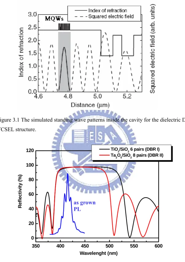
Figure 3.1 The simulated standing wave patterns inside the cavity for the
dielectric DBRs VCSEL structure………49
Figure 3.2 Measure spectral reflectivity of 6 pairs of SiO
2/TiO
2DBR and
8 pairs of SiO
2/Ta
2O
5DBR. The PL spectrum of the as grown cavity consists
of 10 pairs of 5 nm GaN barriers and 3 nm In
0.1Ga
0.9N wells………….…49
Figure 3.3 The layer structure used for calculation of standing wave
patterns. The structure was constructed according to the fabricated dielectric
DBRs VCSELs………50
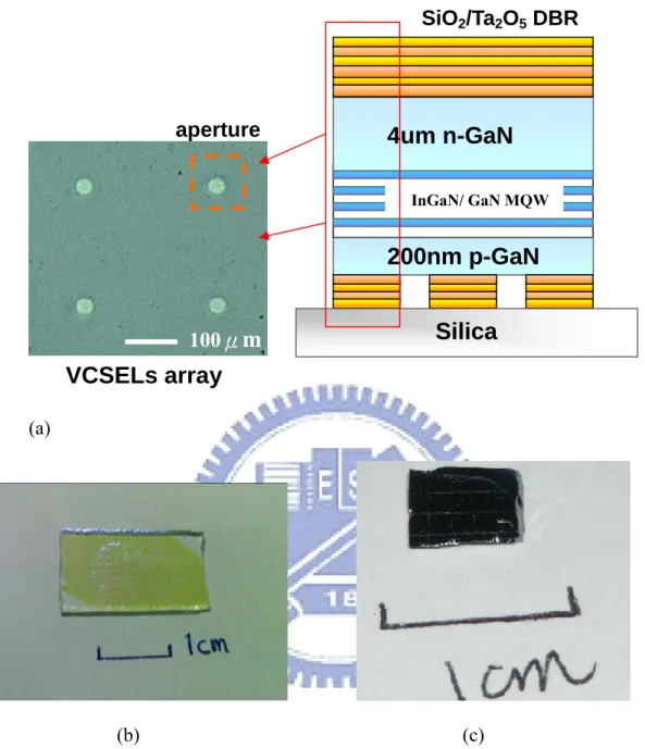
Figure 3.4 Fabrication of the GaN-based dielectric DBRs VCSEL…..51
Figure 3.5 (a) The left picture is the microscopic image of a fabricated
2x2 VCSEL array. The circular areas are the locations of VCSELs with
DBRs, also serving the emission apertures. (b)、(c) A photograph of the
fabricated VCSEL on a silica host substrate and a Si substrate,
respectively………...52
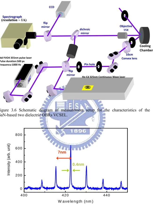
Figure 3.6 Schematic disgram of measurement setup for the
characteristics of the GaN-based two dielectric DBRs VCSEL……….…..53
Figure 3.7 Spontaneous emission spectrum below threshold condition
shows multiple cavity modes………...53
Figure 3.8 Spectral evolution of the VCSEL emission different pumping
levels………54
Figure 3.9 Laser emission intensity obtained from the emission spectra
as a function of pumping energy at room temperature. The inset represents
one of the lasing conditions,
whose pumping power is 0.89mW.…………54
Figure 3.10 Far field pattern of the VCSEL………...…55
Figure 3.11 The angle dependent laser intensity………55
Figure 3.12 Temperature dependence of the lasing threshold of the
VCSEL……….…56
Figure 3.13 Photoluminescence spectra of the GaN-based VCSEL under
different pumping power levels at 80 K………...…………57
Figure 3.14 Gain spectra of the VCSEL under different pumping power
levels at 80 K………..….57
Figure 3.15 Pumping carrier density dependence of the peak gain of the
lasing mode for different temperature………..58
Figure 3.16 The α-factor value at different temperature temperature…58
Figure 3.17 (a) Micro-PL intensity mapping image of the VCSEL
aperture. (b) Fine micro-PL scan inside the square area in (a)………59
Figure 3.18 PL spectra of highest PL intensity point (A) and the lower
PL intensity point (B)………..…60
Figure 3.19 Photoluminescence spectra of the GaN-based VCSEL under
different pumping power levels at 80k (a) the bright areas (A), (b) the dark
areas (B)………..……61
Figure 3.20 Gain spectra of the VCSEL under different pumping power
levels at 80k.(a) the bright areas (A), (b) the dark areas (B)……...………62
Figure 3.21 Pumping carrier density dependence of the peak gain of the
lasing mode for different temperature (a) the bright areas (A), (b) the dark
areas (B)………..…63
Chapter 4
Figure 4.1 Schematic diagram of measurement setup………..………69
Figure 4.2 The PL spectra of optically pumped GaN/InGaN surface
emitting microcavity (a) PL spectra at various pump power levels. The GaN
and InGaN/GaN QW transitions are both excited. The resonant spacing
decreases by almost a factor of five from 470 nm to 370 nm. (b) A zoom in
spectrum around GaN transition wavelength region. (c) (d) Typical multiple
Lorentzian profile fitting along with the sums of the fitted profiles
superimposed on PL spectra……….70
Figure 4.3 Phase shift and reflectance of DBR………..………72
Figure 4.4 The index of refraction measured by ellipsometer (blue curve)
is fitted by a theoretical index dispersion equation (red curve)………72
Figure 4.5 The effective index from PL resonant peaks (blue square
legend) are fitted by a theoretical index dispersion equation (red curve)…73
Figure 4.6 The red square legends are the observed multimode energy
positions plotted versus equally spaced wave numbers. The blue line is the
fitted curve based on cavity polariton dispersion equation. The two straight
lines are the exciton and photon energies obtained from fitting parameters.
The black triangle legends are the corresponding cavity photon modes….74
Chapter 1
Introduction and Motivation
1.1 GaN-based materials and motivation
Group III-nitride wide-band-gap semiconductors have recently attracted considerable interest owing to their applications in optoelectronics devices, such as blue-light-emitting diodes (LEDs) and laser diodes (LDs).GaN based-compound in optical devices that are active in the blue/green and ultraviolet (UV) wavelength regions make it a compelling material system for electronic devices capable of operating at high temperature, high power levels, and in harsh environments. In 1993, the first prototype high brightness GaN-based blue LEDs were developed by Nakamura’s group, also they developed the first GaN-based violet LD with an emission wavelength of around 400nm in 1996. From that time, research groups in the laboratories and companies have spent more time on the development of GaN-based devices and many commercial products with various applications were produced. Today, bright blue LEDs based on III-nitrides paved the way for full-color display as well as for the mixing of the three primary colors to obtain white light for illumination by semiconductor LEDs. Short-wavelength LDs based on III-nitrides are essential for high-density optical storage applications because the diffraction-limited optical storage density increases quadratically as the probe laser wavelength is reduced. GaN-based shot-wavelength devices, such as blue LEDs and LDs, are required for a number of applications including solid-state lighting, full-color electroluminescent displays, laser printers, read-write laser sources for high-density information storage on magnetic and optical media, and sources for short-distance optical
of the GaN-based materials due to the high luminescence efficiency, reliability and durability of the semiconductor light-emitting devices.
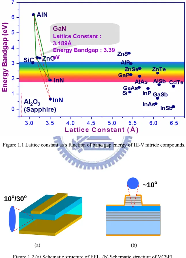
As demonstrated by III-nitride bright blue LEDs and LDs, all III-nitride-based devices must take advantage of heterojunctions and QWs. InGaN and AlGaN are direct band gap semiconductor alloys with energy band gap varying from 0.7 to 3.4 eV (InGaN) and 3.4 to 6.2 eV (AlGaN), with a predominant wurtzite structure for both alloys at all composition, as shown in Figure 1.1. Thus, red- to ultraviolet-emitting devices are possible to be fabricated by using AlGaInN. It is well known that localized exciton recombination is the dominant optical process in many semiconductor alloys at low temperature, including CdSSe, GaAsP, and CdMnTe alloys. The unique properties of III-nitrides make them have many particularly problemsin growth, characterization, and device fabrications. Substrate is an important issue for III-V ntride material growth. Comparing to the GaAs material system, GaN-based substrate generally have a large lattice mismatch. Due to the lack of GaN substrates, III-nitride epilayers are most commonly grown on SiC or sapphire substrates, which contain a high dislocation density of the order of 108~1010/cm2. Nevertheless, SiC is more proper than sapphire for the
substrate for GaN since it has small lattice mismatch. However, the cost of a SiC substrate is very expensive. Therefore, sapphire becomes a suitable and alternative substrate for GaN growth. The first progress used AlN [1.1, 1.2] or GaN [1.3, 1.4] nucleation layers to get high-quality GaN films including of high mobility and strong photoluminescence (PL) intensity. For the LEDs and LDs p/n layers are used to inject holes and electrons into the active layers, therefore, both p-type and n-type conductivity control are required to fabricate those devices. N-type GaN was easy to form but it was
impossible to obtain p-type GaN films for a long period [1.5, 1.6]. Nevertheless, Amano et al [1.7] in 1989 and Nakamura et al [1.8, 1.9] in 1992 obtained the low-resistivity p-type GaN films. Optical properties of III-nitride quantum wells (QWs) are more complicated in comparison with other better understood III-V QWs due to the lack of GaN substrates and the large energy band gap offset and lattice mismatch between the well and the barrier materials. The main progress was the growth of InGaN film which is the most important compound semiconductor among III–V nitride compounds because InGaN active layers emit light by the recombination of the injected electrons and holes in the InGaN. An InGaN multiquantum-well (MQW) structure and confirmed an enhanced strong PL intensity from the quantized energy levels of the InGaN well layer with a thickness of 25 Å for the first time [1.10]. A small amount of indium added to the GaN could result a strong band-to-band emission from green to ultraviolet (UV) by changing the In content of InGaN. While the GaN without indium cannot emit a strong band-to-band emission at room-temperature. Therefore, indium content is very important which reason is considered to be related to deep localized energy states [1.11-1.15].
Many efforts were done on improving the internal quantum efficiency (IEQ) and light extraction efficiency (LEE) of GaN-based LEDs. Therefore, how to reduce the dislocation or defect and improve the light extraction efficiency is an important issue. For example, textured or roughtened surfaces [1.16], substrate shaping [1.17], thin-film LED [1.18], flip-chip LED [1.19] and photonic crystal on LED [1.20], ect.
1.2 GaN-based laser diodes
At present, the main focus of III-V nitride research is to develop a commercially viable current-injection laser diode which operates by continuous-wave (CW) at room
temperature. Recent developments have yielded on optically pumped stimulated emission from GaN films [1.21, 1.22], InGaN films [1.23-1.26], AlGaN/InGaN double heterostructures [1.27] and GaN/AlGaN double heterostructures [1.28, 1.29]. The RT violet edge-emitting laser (EEL) with InGaN MQW GaN/AlGaN-based heterostructures under pulsed operation were achieved [1.30]. After that, many groups have reported pulsed operation of EELs [1.31-1.38] and high-power LDs fabricated using epitaxially laterally overgrown GaN (ELOG) [1.39] and GaN substrates [1.40]. Also, owing to ensuing continual advances in GaN technology, optically [1.23, 1.41-1.47] and electrically [1.48, 1.49] pumped GaN-based Vertical-cavity surface-emitting lasers (VCSELs) have been reported at low and room temperature.
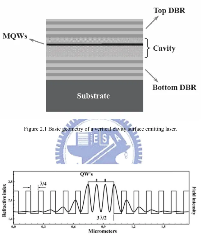
VCSELs are different from EELs in device structure, it is another type of semiconductor lasers. The optical cavity length of VCSELs and EELs are of about 1 μm and 300 μm respectively. Therefore, VCSEL structures can emit a single longitudinal mode with a symmetrically circular beam due to a smaller optical mode volume compared to the EELs. Recently, the realization of GaN-based blue-violet-light VCSELs has attracted much attention because of their many advantages over EELs, including a circular beam, a small beam divergent angle, light emission in the vertical direction, and two-dimensional arrays at the wafer level, as shown in Figure 1.2. In particular, the use of two-dimensional arrays of the blue VCSEL could reduce the read-out time in high density optical storage and increase the scan speed in high-resolution laser printing technique. Several groups have reported optically pumped GaN-based VCSELs using different kinds of vertical resonant cavity structure [1.50-1.59]. VCSELs in many respects outperform EELs diodes. These devices have already become the dominating transmitter source for
commercial high-speed optical interconnects operating in the 800 to 1000nm wavelength regime, and the emergence of 1.3 and 1.55 μm long-wavelength VCSELs on the market is eagerly awaited. Additionally, the strong field in the VCSEL microcavity can facilitate the investigation of the cavity quantum electrodynamics effect such as single photon and polariton emission, controlled spontaneous emission, and low threshold or thresholdless lasing [1.60-1.62].
1.3 GaN-based laser microcavities
A typical microcavity (MC) consists of a few half wavelength lengths cavity and a pair of high-reflectivity distributed Bragg mirrors (DBRs) are necessary for reducing lasing threshold. The planar semiconductor MCs in the strong coupling regime [1.63] have attracted a good deal of attention owing to their potential to enhance and control the interaction between photons and excitons, which leads to cavity polaritons. Beyond the standard VCSELs mentioned above, another type of laser, polariton laser is very attractive owing to its nearly thresholdless operation through Bose-Einstein condensation using cavity polaritons whose genesis lies in the interaction between photons and excitons.Polariton lasers have attracted much attention because of their many advantages over conventional lasers, including the reason that light is emitted by a macroscopic population of exciton-polaritons accumulated in the lowest energy state of their spectrum due to stimulated scattering. Note that no population inversion is needed in a polariton laser. Polariton lasers, MC structures, operative in the strong coupling regime can produce ultra-coherent light. Emission of photons by a polariton laser is a tunneling effect: light passes through a mirror from inside the cavity (where it is incorporated in an exciton-polariton condensate) to outside the cavity (where it becomes conventional light
composed of free photons). Thus, polariton lasers have no threahold linked to the population inversion. Amplification of light in polariton lasers is governed by the ratio between the lifetime of exciton polaritons and their relaxation time towards the condensate. This relaxation has a stimulated character in polariton lasers, which is why it can be quite rapid.
Polariton lasing at high temperatures requires other material systems in which excitons actually survive at that temperature. The semiconductor-based MCs such as GaN came to attract increasing attention to room temperature polariton devices, such as polariton lasers, polariton LEDs, and polariton parametric amplifiers owing to the large exciton binding energies and oscillator strengths. Recently, room temperature polariton lasing has been observed in a bulk-GaN MC [1.64], and multi quantum well (MQW) MC [1.65]. Since the study of polariton induced nonlinear phenomena is in its early stage, electrically injected polariton lasers are awaiting further development. However, the optically pumped experiments, which have been successful, form the stepping stone for electrical injection.
1.4 An overview of the thesis
Chapter 2 outlines the GaN-based VCSEL. We fabricating a GaN-based VCSEL and overview the three main types of propertied GaN-based VCSELs. The reasons for using VCSEL structure with two dielectric mirrors in the thesis are presented. We presents the structure and designing issues of the GaN-based VCSELs with two dielectric mirrors. The spectral reflectivity of the SiO2/TiO2 and SiO2/Ta2O5 DBRs are calculated by
transfer matrix method. The standing optical field in the resonant cavity were also simulated in order to design the epitaxial structure for obtaining a optimal optical gain.
The fabrication steps of the two dielectric DBRs VCSELs are also demonstrated. Basic theory of the laser lift-off technique used in our work is reviewed and introduced. We have introduced a theory of the semiconductor microcavity and discussed the interaction between excitons and photons in the strong coupling regime. We also explore the Bose Einstein condensation characteristics. for polariton at the same time.
Chapter 3 shows the performance of the optically pumped GaN-based VCSELs. The threshold condition, cavity Q factor, characteristic temperature, polarization of the laser emission, divergent angle, gain and linewidth enhancement factor are characterized and discussed. The inhomogeneous indium composition in the InGaN/GaN MQWs are observed.
Chapter 4 present the frequency spacing between adjacent PL peaks decreases by almost a factor of five from 470 nm to 370 nm. We use the intrinsic material index dispersion and polariton dispersion to fit the experimental data, it shows that the latter fitting curve is much better than the former one. It is shown a very strong polariton dispersion in a multimode GaN surface emitting microcavity at room temperarure.
In the final chapter, chapter 5, an overview of this hesis and directions of future works are given and proposed.
InN
Figure 1.1 Lattice constant as s function of band gap energy of III-V nitride compounds.
(a) (b)
Figure 1.2 (a) Schematic structure of EEL. (b) Schematic structure of VCSEL.
10
o/30
oReference
[1.1] S. Yoshida, S. Misawa and S. Gonda: Appl. Phys. Lett. 42, 427 (1983)
[1.2] H. Amano, N. Sawaki, I. Akasaki and T. Toyoda: Appl. Phys. Lett. 48, 353 (1986) [1.3] S. Nakamura and G. Fasol: The Blue Laser Diode (Heidelberg: Springer,1997) [1.4] S. Nakamura: Jpn. J. Appl. Phys. 30, L1705 (1991)
[1.5] S. Strite and H. Morko: J. Vac. Sci. Technol. B 10, 1237 (1992) [1.6] F. A. Ponce and D. P. Bour: Nature 386, 351 (1997)
[1.7] H. Amano, M. Kito, K. Hiramatsu and I. Akasaki: Japan. J. Appl. Phys. 28, L2112 (1989)
[1.8] S. Nakamura, T. Mukai , M. Senoh and N. Iwasa: Japan. J. Appl. Phys. 31, L139 (1992)
[1.9] S. Nakamura, N. Iwasa, M. Senoh and T. Mukai: Japan. J. Appl. Phys. 31, 1258 (1992)
[1.10] S. Nakamura , T. Mukai, M. Senoh, S. Nagahama and N. Iwasa: J. Appl. Phys. 74, 3911 (1993)
[1.11] S. Chichibu, T. Azuhata, T. Sota and S. Nakamura: Appl. Phys. Lett. 69, 4188 (1996)
[1.12] S. Chichibu, T. Azuhata, T. Sota and S. Nakamura: Appl. Phys. Lett. 70, 2822 (1997)
[1.13] Y. Narukawa, Y. Kawakami, Sz Fujita, Sg Fujita and S. Nakamura: Phys. Rev. B 55, 1938 (1997)
[1.14] Y. Narukawa, Y. Kawakami, M. Funato, Sz Fujita, Sg Fujita and S. Nakamura: Appl. Phys. Lett. 70, 981 (1997)
[1.15] S. Chichibu, K. Wada and S. Nakamura: Appl. Phys. Lett. 71, 2346 (1997) [1.16] C. Huh, K. S. Lee, E. J. Kang and S. J. Park: J. Appl. Phys. 93, 9383 (2003) [1.17] Compound Semiconductors 7(1), 7 (2001).
[1.18] W. S. Wong and T. Sands: Appl. Phys. Lett. 75, 1036 (1999)
[1.19] J. J. Wierer, D. A. Steigerwald, M. R. Krames, J. J. O’Shea, M. J. Ludowise, G. Christenson, Y.-C. Shen, C. Lowery, P. S. Martin, S. Subramanya, W. Gotz, N. F. Gardner, R. S. Kern, and S. A. Stockman: Appl. Phys. Lett. 78, 3379 (2001)
[1.20] J. Shakya, K. H. Kim, J. Y. Lin and H. X. Jiang: Appl. Phys. Lett. 85, 142 (2004) [1.21] H. Amano, T. Asahi and I. Akasaki: Jpn. J. Appl. Phys. 29, L205 (1990)
[1.22] A.S. Zubrilov, V.I. Nikolaev, D.V. Tsvetkov, V.A. Dmitriev, K.G. Irvine, J.A. Edmond and C.H. Carter: Appl. Phys. Lett. 67, 533 (1995)
[1.23] T. Someya, K. Tachibana, J. Lee, T. Kamiya, and Y. Arakawa: Jpn. J. Appl. Phys., vol. 37, pp. L1424-L1426, Dec. 1998.
[1.24] T. Someya, R. Werner, A. Forchel, M. Catalano, R. Cingolani, and Y. Arakawa: Science, vol. 285, pp. 1905-1906, Sep. 1999.
[1.25] M.A. Khan, S. Krishnankutty, R.A. Skogman, J.K. Kuznia and D.T. Olson: Appl, Phys. Lett. 65, 520 (1994).
[1.26] S.T. Kim, H. Amano and I. Akasaki: Appl. Phys. Lett. 67, 267 (1995).
[1.27] H. Amano, T. Tanaka, Y. Kunii, K. Kato, S.T. Kim and I. Akasaki: Appl. Phys. Lett. 64, 1377 (1994).
[1.28] R.L. Aggarwal, P.A. Maki, R.J. Molnar, Z.L. liau and I. Melngailis: J. Appl. Phys. 79, 2148 (1996).
Botchkarev, and H. Morkoc: Appl. Phys. Lett. 68,1820 (1996).
[1.30] S. Nakamura, M. Senoh , S. Nagahama, N. Iwasa, T. amada, T. Masushita, H. Kiyoku and Y. Sugimoto: Jpn. J. Appl. Phys. 35, L74 (1996)
[1.31] K. Itaya: Japan. J. Appl. Phys. 35, L1315 (1996)
[1.32] G. E. Bulman, K. Doverspike , S. T. Sheppard, T. W. Weeks, H. S. Kong, H. M. Dieringer, J. A. Edmond, J. D. Brown, J. T. Swindell and J. F. Schetzena: Electron. Lett. 33, 1556 (1997)
[1.33] M. P. Mack, A. Abare, m. Aizcorbe, P. Kozodoy, S. Keller, U. K. Mishra, L. Coldren and S. DenBaars: 1997 MRS Internet J. Nitride Semicond. Res. 2 41 (available from http://nsr.mij.mrs.org/2/41/)
[1.34] A. Kuramata, K. Domen, R. Soejima, K. Horino, S. Kubota and T. Tanahashi: Jpn. J. Appl. Phys. 36, L1130 (1997)
[1.35] F. Nakamura et al 1998 J. Crystal Growth 189/190 84
[1.36] M. Kneissl, D. P. Bour, N. M. Johnson, L. T. Romano, B. S. Krusor, R. Donaldson, J. Walker and C. D. Dunnrowicz: Appl. Phys. Lett. 72, 1539 (1998)
[1.37] H. Katoh, T. Takeuchi, C. Anbe, R. Mizumoto, S. Yamaguchi, C. Wetzel, H. Amano, I. Akasaki, Y. Kaneko and N. Yamada: Jpn. J. Appl. Phys. 37. L 444
(1998)
[1.38] Nanfang Yu, Romain Blanchard, Jonathan Fan, Federico Capasso, Tadataka Edamura, Masamichi Yamanishi, and Hirofumi Kan: Appl. Phys. Lett. 93, 181101 (2008) [1.39] S. Nakamura: Japan. J. Appl. Phys. 37, L627 (1998)
[1.40] S. Nakamura: Japan. J. Appl. Phys. 37, L309 (1998)
Science, vol. 285, pp. 1905-1906, Sep. 1999.
[1.42] Y. –K. Song, H. Zhou, M. Diagne, I. Ozden, A. Vertikov, A. V. Nurmikko, C. Carter-Coman, R. S. Kern, F. A. Kish, and M. R. Krames: Appl. Phys. Lett., vol. 74, pp. 3441-3443, Jun. 1999.
[1.43] H. Zhou, M. Diagne, E. Makarona, J. Han, K. E. Waldrip, and J. J. Figiel: Electron. Lett., vol. 36, pp. 1777-1779, Oct. 2000.
[1.44] Y. –K. Song, H. Zhou, M. Diagne, A. V. Nurmikko, R. P. Schneider, Jr., C. P. Kuo, M. R. Krames, R. S. Kern, C. Carter-Coman, and F. A. Kish: Appl. Phys. Lett., vol. 76, pp. 1662-1664, Mar. 2000.
[1.45] T. Tawara, H. Gotoh, T. Akasaka, N. Kobayashi, and T. Saitoh: Appl. Phys. Lett., vol. 83, pp. 830-832, Aug. 2003.
[1.46] E. Feltin, G. Christmann, J. Dorsaz, A. Castiglia, J. –F. Carlin, R. Butté, N. Grandjean, S. Christopoulos, G. Baldassarri Höger von Högersthal, A. J. D. Grundy, P. G. Lagoudakis, and J. J. Baumberg: Electron., Lett., vol. 43, pp. 924-925, Aug. 2007.
[1.47] A. Castiglia, D. Simeonov, H. J. Buehlmann, J. –F. Carlin, E. Feltin, J. Dorsaz, R. Butté, and N. Grandjean: Appl. Phys. Lett., vol. 90, pp. 033514/1-3, Jan. 2007.
[1.48] T. -C. Lu, C. -C. Kao, H. -C. Kuo, G. -S. Huang, and S. -C. Wang: Appl. Phys. Lett., vol. 92, pp. 141102/1-3, Apr. 2008.
[1.49] Y. Higuchi, K. Omae, H. Matsumura, and T. Mukai: Appl. Phys. Express., vol. 1, 121102/1-3, Dec. 2008
[1.50] J. M. Redwing, D. A. S. Loeber, N. G. Anderson, M. A. Tischler, and J. S. Flynn: Appl. Phys. Lett. 69, 1 (1996)
37, L1424 (1998)
[1.52] Y.-K. Song, H. Zhou, M. Diagne, I. Ozden, A. Vertikov, A. V. Nurmikko, C. Carter-Coman, R. S. Kern, F. A. Kish, and M. R. Krames: Appl. Phys. Lett. 74, 3441 (1999)
[1.53] T. Someya, R.Werner, A. Forchel, M. Catalano, R. Cingolani and Y.Arakawa: Science, 285, 1905 (1999)
[1.54] T. Tawara, H. Gotoh, T. Akasaka, N. Kobayashi and T. Saitoh: Appl. Phys. Lett., 83, 830 (2003)
[1.55] Y.-K. Song, H. Zhou, M. Diagne, A. V. Nurmikko, R. P. Schneider, Jr., C. P. Kuo, M. R. Krames, R. S. Kern, C. Carter-Coman and F. A. Kish: Appl. Phys. Lett., 76, 1662 (2000)
[1.56] H. Zhou, M. Diagne, E. Makarona, A. V. Nurmikko, J. Han, K. E. Waldrip and J. J. Figiel: Electron. Lett., 36,1777 (2000)
[1.57] T. Someya, K. Tachibana, J. Lee, T, Kamiya and Y. Arakawa: Jpn. J. Appl. Phys., 37, L1424 (1998)
[1.58] J. M. Redwing, D. A. S. Loeber, N. G. Anderson, M. A. Tischler, and J. S. Flynn: Appl. Phys. Lett., 69, 1 (1996)
[1.59] S. H. Park, J. Kim, H. Jeon, T. Sakong, S. N. Lee, S. Chae, Y. Park, C. H. Jeong, G. Y. Yeom, and Y. H. Cho: Appl. Phys. Lett., 83, 2121 (2003)
[1.60] M. Pelton, C. Santori, J. Vuckovic, B. Zhang, G. S. Solomon, J. Plant, and Y. Yamamoto: Phys. Rev. Lett. 89, 233602 (2002)
[1.61] H. Deng, G. Weihs, C. Santori, J. Bloch, and Y. Yamamoto: Science 298, 199 (2002)
[1.62] T. Kobayashi, T. Segawa, A. Morimoto, and T. Sueta: presented at 43rd Fall Meet. Japan Society of Applied Physics, Tokyo, September, 1982
[1.63] M. S. Skolnick, T. A. Fisher, and D. M. Whittaker: Semicond. Sci. Technol., vol. 13, pp. 645-669, Mar. 1998.
[1.64] S. Christopoulos, G. Baldassarri Höger von Högersthal, A. J. D. Grundy, P. G. Lagoudakis, A. V. Kavokin, J. J. Baumberg, G. Christmann, R. Butté, E. Feltin, J. –F. Carlin, and N. Grandjean: Phys. Rev. Lett., vol. 98, pp. 126405/1-4, Mar. 2007.
[1.65] G. Christmann, R. Butté, E. Feltin, J. –F. Carlin, and N. Grandjean: Appl. Phys. Lett., vol. 93, pp. 051102/1-3, Aug. 2008.
Chapter 2
Fundamental of GaN-based vertical cavity surface emitting
lasers and semiconductor microcavities
2.1 Vertical cavity surface emitting lasers
2.1.1 Fundamental of VCSELs
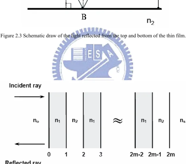
As depicted in Figure 2.1, the typical structure of most VCSELs consist of two parallel reflectors which are distributed Bragg reflectors (DBRs), and a cavity including a multiple quantum wells (MQWs) served as active layer. Besides, diode lasers like the other types of lasers, diode laser contain three ingredients, including Gain medium, pumping source, and resonant cavity. The gain medium consists of a material which normally absorbs incident radiation over some wavelength range of interest. But, if it is pumped by inputting either electrical or optical energy, the electrons within the material can be excited to the higher, nonequilibrium energy level, so that the incident radiation can be amplified rather than absorbed by stimulating the de-excitation of these electrons along with the generation of additional radiation. If the resulting gain is sufficient to overcome the losses of some resonant optical mode of the cavity, this mode is said to have reached threshold, and relatively coherent light will be emitted. Pumping source provides the energy that can excite the electrons within gain medium at lower energy level to higher energy level. It could be either optical or electrical energy. The resonant cavity provides the necessary positive feedback for the radiation being amplified, so that a lasing oscillation can be established and sustained above threshold pumping level. Therefore, the reflectivity necessary to reach the lasing threshold should normally be
higher than 99.9%. Corresponding to the ingredients of a laser, the active layer is the gain medium that amplify the optical radiation in the cavity; the top DBR, bottom DBRs and cavity form a resonant cavity where the radiation can interact with active region and have positive feedback.
An optical cavity or optical resonator is an arrangement of mirrors that forms a standing wave cavity resonator for light waves. Light confined in the cavity reflect multiple times producing standing waves for certain resonance frequencies. The standing wave patterns produced are called modes; longitudinal modes differ only in frequency while transverse modes differ for different frequencies and have different intensity patterns across the cross section of the beam. Recently, the Fabry-Perot cavity are employed in nearly all laser cavity.It is by using the interference of lightreflectedmany times between two coplanar lightly-silvered mirrors. It is a high resolution instrument that has been used today in precision measurement and wavelength comparisons in spectroscopy. Also, the Fabry-Perot cavities can be used to ensure precise tuning of laser frequency. The thickness of the cavity and the position of the MQWs inside the MCs are two key features of the VCSEL devices. Thickness of a cavity decides the resonant wavelength that will lase above threshold condition according to
n N L 2 λ = , where L is cavity length, N is an integral, λ is resonant wavelength and n is the refractive index of the cavity. Usually the resonant wavelength of the cavity is chosen to be equal to the Bragg wavelength, such that the resonant wavelength can encounter the maximum reflectivity of the DBR. Typically, the cavity length of VCSELs is on the order of few half operating wavelengths. In such a short cavity device, the electromagnetic waves
would form standing wave patterns with nodes (electromagnetic wave intensity minima) and anti-nodes (electromagnetic wave intensity maxima) within the GaN microcavity. The location of the InGaN/GaN MQWs with respect to the anti-modes can significantly affect the coupling of laser mode with the cavity field. As the MQWs are well aligned with the cavity field, the more electromagnetic wave interact with the MQWs result in more photon generated in the cavity, that is optical gain of resonant mode is increased. The proper alignment of the MQWs region with the anti-nodes of the cavity standing wave field patterns will enhance the coupling and reduce laser threshold condition. As a result, the precise layer thickness control in the VCSEL fabrication is important. Therefore, optical cavities are designed to have a large Q factor; a beam will reflect a very large number of times with little attenuation and the frequency linewidth of the beam is very small indeed compared to the frequency of the laser.
2.1.2 Distributed Bragg reflector
In the GaN-based VCSEL structure, a micro cavity with a few λ in the optical
thickness and a pair of high reflectivity (above 99%) distributed Bragg reflectors (DBRs) are necessary for reducing the lasing threshold. Recently, several groups have reported optically pumped GaN-based VCSELs mainly using three different kinds of vertical resonant cavity structure forms: (1) monolithically grown vertical resonant cavity consisting of epitaxially grown III-nitride top and bottom DBRs (epitaxial DBR VCSEL), (2) vertical resonant cavity consisting of dielectric top and bottom DBR (dielectric DBR VCSEL). (3) vertical resonant cavity consists of an epitaxially grown III-nitride top DBR and a dielectric DBR (hybrid DBR VCSEL).
VCSELs, dielectric DBRs was used in the GaN-based VCSEL in this study. Distributed Bragg reflector (DBR) consists of an alternating sequence of high and low refractive index layers with quarter-wavelength thickness, as Figure 2.2 [2.1]. Therefore, it’s necessary to know the theory of quarter-wave layer before discussing the DBRs. Now, consider the simple case of a transparent plate of dielectric material having a thickness d and refractive index n
f, as shown in Figure 2.3. Suppose that the film is nonabsorbing and
that the amplitude-reflection coefficients at the interfaces are so low that only the first two reflected beams (both having undergone only one reflection) need be considered. The reflected rays are parallel on leaving the film and will interference at image plane. The optical path difference (P) for the first two reflected beam is given by
P=nf[(AB)+(BC)]−n1(AD) (2.1) And since
( ) ( )
t d BC AB θ cos = = (2.2)( ) ( )
AD = AC sinθi (2.3)Using Snell’s Law n1sinθi =nf sinθt (2.4) Then
( ) ( )
f t n n AC AD sinθ 1 = (2.5) also( )
AD =2dtanθt (2.6)The eq. (2.1) becomes t f t
t f d n d n P θ θ θ (1 sin ) 2 cos cos 2 2 = − = (2.7) The corresponding phase difference (δ) associated with the optical path length difference is then just the product of the free-space propagation number and P, that is, K0P.
as n1=n2=n. It is noted that no matter nf is greater or smaller than n, there will be a
relative phase shift π radians. Therefore, 4 ) 1 2 ( cosθ = m+ λ0 d t (m=0,1,2,3,…) (2.8) π λ θ π δ = − ± 0 2 2 2 2 sin ) ( 4 nf nf n i (2.9) The interference maximum of reflected light is established when δ=2mπ, in other words, an even multiple of π. In that case, eq. (2.8) can be rearranged; and the interference minimum of reflected light when δ = (2m±1) π, in other words, an odd multiple of π. In that case eq. (2.9) also can be rearranged.
⎪ ⎪ ⎩ ⎪ ⎪ ⎨ ⎧ = = = + = ] [min ,...) 3 , 2 , 1 , 0 ( , 4 2 cos ] [max ,...) 3 , 2 , 1 , 0 ( , 4 ) 1 2 ( cos 0 0 imum m n m d imum m n m d f t f t λ θ λ θ (2.10)
Therefore, for an normal incident light into thin film, the interference maximum of reflected light is established when d = λ0/4n
f (at m=0). Based on the theory, a periodic
structure of alternately high and low index quarter-wave layer is useful to be a good reflecting mirror. This periodic structure is also called Distributed Bragg Reflectors (DBRs). Therefore, the concept of DBR is that many small reflections at the interface between two layers can add up to a large net reflection. At the Bragg frequency the reflections from each discontinuity add up exactly in phase. Spectral-dependent of the reflectivity can be calculated by the transfer-matrix method [2.2]. Considering a layer if dielectric material b which is clad between two layers a and c. A transverse electromagnetic wave at normal incidence propagates throught the layer in z direction.
Taking the electric and magnetic (E and H) fields into consideration by Maxwell’s equation, a transmission matrix relating these fields can be written as
⎟ ⎟ ⎠ ⎞ ⎜ ⎜ ⎝ ⎛ ⎟⎟ ⎟ ⎟ ⎟ ⎠ ⎞ ⎜⎜ ⎜ ⎜ ⎜ ⎝ ⎛ = ⎟ ⎟ ⎠ ⎞ ⎜ ⎜ ⎝ ⎛ ) 0 ( ) ( ) cos( ) sin( ) sin( ) cos( ) 0 ( ) 0 ( 0 0 H d E d k d k jn d k n j d k H E b b b b b b η η (2.11)
In the equation, nb is the refractive index of layer b and ηo the impedance of free space,
j is the unit imaginary number, kb is the phase propagation constant in layer b,
λ π
b
b n
k = 2 , where λ is the wavelength in free space. Here, the absorption was not considered in this discussion. For a multilayer, a matrix Mi is formed for each layer i of thickness di in the
stack. By considering the effect of all layers with summation length of each layers L, a matrix M relates to input and output fields ca be obtained,
⎪ ⎪ ⎪ ⎩ ⎪ ⎪ ⎪ ⎨ ⎧ ⎟ ⎟ ⎟ ⎟ ⎠ ⎞ ⎜ ⎜ ⎜ ⎜ ⎝ ⎛ = = ⎟⎟ ⎠ ⎞ ⎜⎜ ⎝ ⎛ = ⎟⎟ ⎠ ⎞ ⎜⎜ ⎝ ⎛
∏
22 21 12 11 ) ( ) ( ) 0 ( ) 0 ( m m m m M M L H L E M H E i i (2.12)The reflection coefficient r of the stack is:
22 21 12 0 11 0 22 21 12 0 11 0 m Y m m Y m Y m Y m m Y m Y r s s + + + − − + = (2.13)
where the Y is wave admittance and o and s refer to the incident and substrate respectively. If we have a layer of index n l between layer o and s of lower under, then the
reflection from interface has a phase of π radians relative to the incident wave, because of the positive index step. If the thickness of the layer is a quarter wavelength the two
second reflection. For a stack with many alternate 1/4 wave (or (n/2+1/4) wave, n integral) layers of low and high index, all interfacial reflections will add in phase.
For a Bragg reflector made from quarter wavelength layers of indices n1 and n2,as
shown in Figure 2.4, the maximum reflectivity R at resonant wavelength, also denoted as Bragg wavelength (λB), of a stack with m non-absorbing pairs can be expressed by:
2 2 2 1 0 2 2 1 0 ) ( 1 ) ( 1 ⎥ ⎥ ⎥ ⎥ ⎦ ⎤ ⎢ ⎢ ⎢ ⎢ ⎣ ⎡ + − = m s m s n n n n n n n n R (2.14)
The no and ns in the equation are the refractive indices of incident medium and substrate,
respectively and m is pair numbers of the DBR. Layer thicknesses L1,2 have to be chosen
as L1,2=λ /(4nB 1,2). The maximum reflectivity of a DBR therefore increases as the
increasing difference in refractive indices and pair number of DBR. A broad spectral plateau of high reflectivity, denoted as a stop-band, appear around the Bragg wavelength, the width of which can be estimate as [2.3]
eff B sb n n π λ λ ≈ Δ
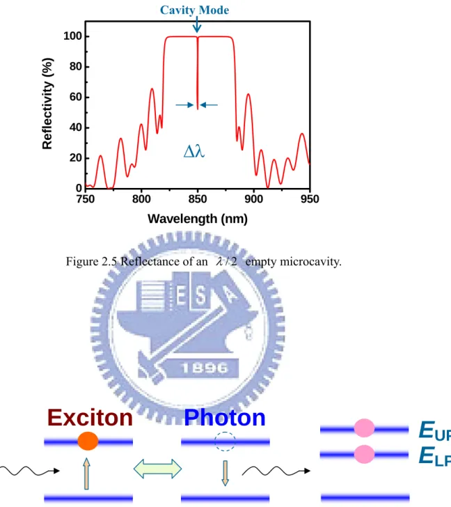
Δ 2 . A wide stop-band provides a larger tolerance between the designed λ and the main wavelength of the cooperated B MQWs, this is another important reason for us to use dielectric DBRs as mirrors in our VCSEL structure. When two such high-reflectance DBRs are attached to a layer with an optical thickness integer times ofλc/2 (λc ≈λ), a cavity resonance is formed at λc, leading to a sharp increase of the transmission T at λc:
) 2 ( sin 4 ] 1 [ ) 1 )( 1 ( 2 2 1 2 2 1 2 1 φ R R R R R R T + − − − = (2.15)
If(R1 ≈R2 =R), ) 1 2
1
( −R 2 ≤T ≤ depending on φ. One characteristic parameter of the cavity quality is the cavity quality factor Q defines as:
2 / 1 2 1 4 / 1 2 1 ) /( 1 ) ( R R R R Q c c π λ λ ≈ Δ = (2.16) Where Δ is the width of the resonance. An ideal cavity has Q = ∞ . If the cavity λc length is λ/2, Q is the average number of round trips a photon travels inside the cavity before it escapes. Figure 2.5 shows an example of the reflection spectrum of a cavity. The high-reflectivity or stop band of a DBR depends on the difference in refractive index of the two constituent materials, n △ (≣n1-n2). We can calculate by requiring the
same optical path length normal to the layers for the DBR and the effective medium. The effective refractive index is then given by
1 2 1 1 1 2 − ⎟⎟ ⎠ ⎞ ⎜⎜ ⎝ ⎛ + = n n neff (2.17) For DBRs, the optical wave penetrates into the reflector by one or several quarter-wave pairs. Only a finite number out of the total number of quarter-wave pairs are effective in reflecting the optical wave. The effective number of pairs seen by the wave electric field is given by ⎟⎟ ⎠ ⎞ ⎜⎜ ⎝ ⎛ + − − + = 2 1 2 1 2 1 2 1 tanh 2 2 1 n n n n m n n n n meff (2.18) For very thick DBRs (m→∞) the tanh function approaches unity and one obtains
2 1 2 1 2 1 n n n n meff − + ≈ (2.19) Also, the penetration depth is given by
) 2 tanh( 4 2 1 mr r L L Lpen = + (2.20) where r = (n1-n2)/ (n1+n2) is the amplitude reflection coefficient.
For a large number of pairs (m→∞), the penetration depth is given by
2 1 2 1 2 1 2 1 4 4 n n n n L L r L L Lpec − + + = + ≈ (2.21) Comparison of eqs. (2.17) and (2.19)
) ( 2 1 2 1 L L m Lpen = eff + (2.22) The factor of (1/2) in Eq. (2.20) is due to the fact that m applies to effective number of eff periods seen by the electric field whereas applies to the optical power. The optical power is equal to the square of the electric field and hence it penetrates half as far into the mirror. The effective length of a cavity consisting of two DBRs is thus given by the sum of the thickness of the center region plus the two penetration depths into the DBRs. So effective cavity length is extended in a semiconductor microcavity as
pen L DBR c eff L L L = +
2.2 Fundamental of semiconductor microcavities
2.2.1 polariton dispersion curve in the strong coupling regime
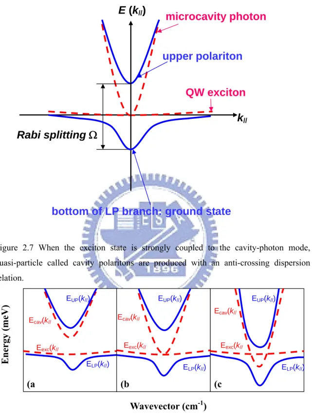
A typical structure of a semiconductor microcavity consisting of a λ/2 cavity layer sandwiched between two DBRs. The planar semiconductor MCs in the strong coupling regime have attracted a good deal of attention and controlled the interaction between photons and excitons, which leads to cavity polaritons, as shown in Figure 2.6. When the exciton state is strongly coupled to the cavity-photon mode, quasi-particle called cavity polaritons are produced with an anti-crossing dispersion relation, as shown in Figure 2.7.
Thus, the elementary excitations of the system are no longer exciton or photon, but a new type of quasi-particle called the polaritons. Polaritons, predicted theoretically by Hopfield [2.4] and Agranovich [2.5] in the end of 1950s, have been extensively studied in bulk semiconductor materials [2.6, 2.7], thin films [2.8, 2.9], quantum wells [2.10, 2.11], and quantum wires and dots [2.12, 2.13]. They can be interpreted as virtual exciton–photon pairs that propagate in the crystal because of a chain of processes of virtual absorption and emission of photons by excitons. The polariton states are true eigenstates of the system, so that once the polaritons are present there are no more pure excitons or photons. The exciton-photon interaction are often described by linear dielectric dispersion model [2.14] or coupled oscillator model [2.15]. The dielectric dispersion is used to described transmissive or reflective spectral experiments. The coupled oscillator model on the other hand is more suitable for describing active PL experiment. In linear regime, the coupled oscillator rate equations for the interaction between a cavity mode a and exciton J are a i a igJ dt da a − + − = γ ω (2.23) J i J iga dt dJ J − Ω + − = γ (2.24) where ω and Ω are photon and exciton frequencies, a and J are the respective decay rates, and g is the interaction constant. The formal solutions of polariton frequencies are
2 / 4 )) ( ) (( 2 / ) ( 2 / ) ( 2 2 , i J a i J a g ex± = Ω+
ω
−γ
+γ
± Ω−ω
−γ
−γ
+ω
, where ±corresponds to the upper and lower branch polariton. We start from the Hamiltonian with the spacial dependence explicitly spelled out,
∑
+ +∫
Ω + +∑ ∫
+ − + = + + = n x n x k k k k k k n exciton photon x u a x J x J x u a g i x J x J a a H H H H n n n n n n ( ) ( ) ( ( ) ( ) ( ) ( )) * . int h h hω
(2.25) where ukn(x) is cavity mode function, kn is the corresponding wave number, and J(x) isexciton field operator. We will discuss the spacial dependence of J(x) and exciton Hamiltonian in more detail shortly. The interaction of photon and exciton with reservoir are neglected for simplicity. These interactions introduce decay to photon and exciton and will be discuss later. g is the exciton-photon interaction constant. Excitons are treated as bosons under low excitation limit [2.16-18]. In the above exciton-photon interaction Hamiltonian Hint, the overlap integral projects exciton field on cavity modes ukn. It can be
shown that, using tight-binding model for exciton wave function, the exciton field in interaction with radiation behaves exactly as a quantized polarization field [2.17]. Similar result could also be obtained from using weak-binding model [2.17]. In our microcavity, excitons in GaN expand the whole cavity defined by two DBR mirrors. Applying the same cavity boundary condition to quantize exciton field, the exciton field is then written in terms of the same cavity mode functions as
J(x) J nukn(x) n
k
∑
= (2.26) where Jkn is the exciton amplitude operator of mode function ukn and satisfies the
commutation relation . The use of cavity mode functions as a basis for exciton field to describe the exciton-photon interaction can be understood from another point of view. To be in the strong interaction regime, one would like to have a
' '
]
,
[
n n n n k kk kJ
J
+=
δ
those excitons with the same cavity mode functions. Therefore, as far as cavity polariton is concerned, it is natural to express exciton field in terms of cavity mode functions. From cavity boundary condition, the cavity mode function ukn satisfies orthogonal
relation . Using this expression, the exciton Hamiltonian is rewritten
as , where Ω nm x k kn
u
mu
=
δ
∫
*∑
Ω
+ n k k nJ
nJ
nh
n is the transition frequency of exciton mode n. Strictly speaking, the exciton transition frequency is wave vector dependent and expression Ωnshould be used. Here, we will treat it as a constant and drop index n from now on since the change of Ωn is small within the range of cavity modes of interest. The Hamiltonian is
thus simplified to n n n n ( n n kn kn) n n k k n k k k k n a a J J i g a J J a H =h
ω
∑
+ +hΩ∑
+ + h∑
+ − + (2.27) The formal operator rate equations are readily obtained asn n n k k n k igJ a i dt da + − =
ω
(2.28) n n n k k kiga
J
i
dt
dJ
+
Ω
−
=
(2.29) One can see that each cavity mode is only coupled to the corresponding exciton mode. There are multiple independent cavity polaritons. The root cause of no cross coupling lies in the fact that mode functions ukn are orthogonal and both photon and exciton fields arebased on the same mode functions. The polariton frequencies for mode ukn are
( )/2 ( )2 4 2 /2
, n n g
pol± = Ω+
ω
± Ω−ω
+ω
(2.30)In particular, the strength of exciton–light coupling is greatly enhanced in microcavities, which results in the so-called strong-coupling regime manifested by anti-crossing of the exciton–polariton modes, observed for the first time by ClaudeWeisbuch et al. [2.19] in 1992. These eigenmodes appeared to be split at the anti-crossing point that defines the strong-coupling regime. Splitting between modes at this point is widely referred to as vacuum-field Rabi splitting or simply Rabi splitting. In the opposite case of the weak-coupling regime, there is no splitting between polariton eigenmodes at the crossing point. The weak-coupling regime is realised, in particular, in VCSELs and vertical cavity light emitting diodes (VCLEDs). For a system of two oscillators there are two possibilities: either they continue to oscillate with the same frequency, or the system starts with two new eigenfrequencies split by a value proportional to the coupling strength between the two oscillators, as shown in Figure 2.7. The first regime is called the weak-coupling regime, and the second is called the strong-coupling regime. If there is no attenuation (appearance of non-zero imaginary parts of the eigenfrequencies) in the system, it is always in the strong-coupling regime. Also, magnetic field can increase the exciton oscillator strength and make it into the strong coupling regime. Note that in semiconductor MCs, strong coupling is usually invisible at room temperarure due to the exciton broadening altered by varying the temperature. Polariton dispersion curves is strongly dependent on the detuning between the bare cavity mode ωc(k)and the bare exciton mode ωex(k) at zero in-plane wave-vector
k=0.The detuning δ is given by ωc(0)- ωex(0). Figure 2.8 shows three typical dispersion
curves of cavity polaritons for positive, zero and negative detunings. One can see that at small k the dispersion of exciton–polaritons in the cavity is essentially parabolic, and can
be characterised by some effective mass, while this mass varies dramatically as a function of detuning. The possibility of tuning the polariton effective mass over a wide range is an important peculiarity of microcavities. Recently, the observed Rabi splittings have reached 50 meV and 56 meV for 3λ/2 and 3λ cavity respectively [2.20, 2.21].
2.2.2 Bose Einstein condensation
Bose Einstein condensation (BEC) [2.22] has been a source of imagination and innovation of physicists ever since its first proposal by Einstein in 1925. The theory mainly focus on describing the characteristics of eigenstates distribution for Bosons, and the most appealing property is that bosons can coexist on the same energy level. In addition, the lower the energy level, the more the particle occupancym, it is far from fermion obeyed “Pauli exclusion principle“. A BEC is a state of matter of a dilute gas of weakly interacting bosons confined in an external potential and cooled to temperatures very near to absolute zero . Under such conditions, a large fraction of the bosons collapse into the lowest quantum state of the external potential, and all wave functions overlap with each other, then quantum effects become apparent in a macroscopic scale.The first application of BEC to a physical system was by London in 1938 [2.23], right after the discovery of superfluid in liquid helium [2.24]. Though we can observe BEC by the characteristics of superfluid, we can not reach the same phenomena at room temperature It has attracted much attention owing to the polariton splitting phenomena of a planar GaAs microcavity discovered by C. Weisbush et al. and M, Nishioka et al. in 1992. In recent years, much attention has been given to the behavior of these cavity polaritons which is the so-called bosonic particles in the strong coupling regime. One area of interest relates to the BEC of cavity polaritons. These polaritons will condense to their
final state with a gain as a result of certain scattering processes, and then coherent light will be emitted from the polaritons in that state. The BEC of the polaritons is expected to yield new scientific fields, such as the coherent manipulation of bosons in a solid state, and be applied to a new generation of devices, such as polariton lasers [2.25], polariton LED [2.26], and polariton amplification [2.27] without threshold or population inversion .
Figure 2.1 Basic geometry of a vertical cavity surface emitting laser.
Figure 2.2 A typical microcavity structure. The central cavity layer having a thickness equal to an integer number of half-wave-lengths of light at the exciton resonance frequency is sandwiched between two Bragg mirrors. A quantum well (several quantum wells) should be embedded in the antinodes of the cavity mode electric field in order to provide the strongest coupling to light.
Figure 2.3 Schematic draw of the light reflected from the top and bottom of the thin film.
Figure 2.4 Schematic of distributed Bragg reflector incorporating m pairs of two mediums with indices n1 and n2.
750 800 850 900 950 0 20 40 60 80 100 Reflectivity (%) Wavelength (nm) Cavity Mode
Δλ
Figure 2.5 Reflectance of an λ/2 empty microcavity.
Exciton
Photon
E
UP
E
LP
k
//E (k
//)
microcavity photon
QW exciton
upper polariton
Rabi splitting
Ω
bottom of LP branch: ground state
Figure 2.7 When the exciton state is strongly coupled to the cavity-photon mode, quasi-particle called cavity polaritons are produced with an anti-crossing dispersion relation.
Wavevector (cm
-1)
Energy (meV)
(a
(b
(c
ELP(k//) EUP(k//)Figure 2.8 Polariton dispersion for different detuning between exciton and photon modes: (a) δ= positive, (b) δ= zero, (c) δ= negative. Dashed lines show the energies of uncoupled exciton and photon modes.
Ecav(k// Ecav(k//
Ecav(k//
Eexc(k// Eexc(k// Eexc(k//
ELP(k//) ELP(k//)
Reference
[2.1] Alexey Kavokin, Guillaume Malpuech: Thin films and nanostructures: cavity polaritons.
[2.2] T. E. Sale: VERTICAL CAVITY SURFACE EMITTING LASERS, (Research Studies Press LTD. 1995)
[2.3] Carl W. Wilmsen, Henryk Temkin and Larry A. Coldren: Vertical-Cavity Surface-Emitting Lasers: Design, Fabrication, Characterization, and Applications, (Cambridge, 1999)
[2.4] J. J. Hopfield, Theory of the contribution of excitons to the complex dielectric constant of crystals: Phys. Rev. 112, 1555 (1958).
[2.5]. V. M. Agranovich, Zh. Eksper. Teoret. Fiz. 37, 1555 (1959).
[2.6] V. M. Agranovich, V. L. Ginzburg: Interscience Publ., London, 1966.
[2.7] E. L. Ivchenko, Spatial dispersion effects in exciton resonance region, in “Excitons” (E. I. Rashba and M. D. Sturge, Eds.). Elsevier, North-Holland, 1982.
[2.8] D. Frölich, A. Kulik, B. Uebbing, A. Mysyrowicz, V. Langer, H. Stolz, W. von der Osten, Coherent propagation and quantum beats of quadrupole polaritons in Cu2O: Phys. Rev. Lett. 67, 2343 (1991).
[2.9]. G. Panzarini, L. C. Andreani, Bulk polariton beatings and two-dimensional radiative decay: Analysis of time-resolved transmission through a dispersive film: Solid State Comm. 102, 505 (1997).
[2.10] L. C. Andreani, F. Tassone, F. Bassani, Radiative lifetime of free excitons in quantum wells: Solid State Comm. 77, 641 (1991).
[2.11] E. L. Ivchenko, Excitonic polaritons in periodic quantum well structures: Sov. Phys. Solid State 33, 1344 (1991).
[2.12] E. L. Ivchenko, A. V. Kavokin, Light reflection from quantum well, quantum wire and quantum dot structures: Sov. Phys. Solid State 34, 1815 (1992).
[2.13] A. D’Andrea, R. Del Sole, Excitons in semiconductor confined systems: Solid State Comm. 74, 1121 (1990).
[2.14] A. P. D. Love, D. N. Krizhanovskii, D. M. Whittaker, R. Bouchekioua, D. Sanvitto, S. Al Rizeiqi, R. Bradley, M. S. Skolnick, P. R. Eastham, R. Andre, et al.: Phys. Rev. Lett. 101 (2008).
[2.15] T. Tawara, H. Gotoh, T. Akasaka, N. Kobayashi, and T. Saitoh: Phys. Rev. Lett. 92, 256402 (2004).
[2.16] L. C. Andreani, G. Panzarini, and J.-M. G´erard: Phys. Rev. B 60, 13276 (1999). [2.17] J. J. Hopfield: Phys. Rev. 112, 1555 (1958).
[2.18] S. Pau, G. Bj¨ork, J. Jacobson, H. Cao, and Y. Yamamoto: Phys. Rev. B 51, 14437 (1995).
[2.19]. C. Weisbuch, M. Nishioka, A. Ishikawa, Y. Arakawa, Observation of coupled exciton–photon mode splitting in a semiconductor quantum microcavity: Phys. Rev. Lett. 69, 3314 (1992).
[2.20] J. Kasprzak, D. D. slonyshkov, R. Andre, L. S. Dang, and G. Malpuech: Phys. Rev. Lett. 101, 146404 (2008).
[2.21] L. C. Andreani, G. Panzarini, and J.-M. G´erard: Phys. Rev. B 60, 13276 (1999). [2.22] Hui Deng: DYNAMIC CONDENSATION OF SEMICONDUCTOR MICROCAVITY POLARITONS (2006).
[2.23] London, F. The ¸-phenomenon of liquid helium and the Bose-Einstein degener- acy: Nature 141, 643 (1938).