國 立 交 通 大 學
電信工程學系
碩士論文
超寬頻射頻傳收機模組
Ultra Wide Band RF Transceiver Module
研究生:江俊賢
指導教授:張志揚 博士
超寬頻射頻傳收機模組
Ultra Wide Band RF Transceiver Module
研 究 生:江俊賢
Student:Chin-Hsien Chiang
指導教授:張志揚 博士 Advisor:Dr. Chi-Yang Chang
國立交通大學
電信工程學系
碩士論文
A Thesis Submitted to Institute of
Communication Engineering
College of Electrical Engineering and Computer Science
National Chiao Tung University
In Partial Fulfillment of the Requirements
for the Degree of Master of Science
In
Communication Engineering
June 2005
Hsinchu, Taiwan, Republic of China
超寬頻射頻傳收機模組
研究生:江俊賢 指導教授:張志揚 博士
國立交通大學電信工程學系
摘要
軍用無線通信系統有別於商用無線通信系統,在使用情景上需
具靈活性、機動性與強韌性。本論文中將介紹超寬頻的射頻傳收機
模組,以完成 UWB 之通訊機。其中包括下列各個微波關鍵性電路,
包含:UWB 射頻濾波器、UWB 功率放大器、UWB 低雜訊放大器、頻率
合成器、寬頻升降頻混頻器、寬頻微波開關、及微波功率偵測器等。
首先,我們將介紹一般的無線通訊系統,並對傳送路徑與接收路徑
分開討論。最後,再實作所有主要的電路元件實作並整合成電路模
Ultra Wide Band RF Transceiver Module
Student:
Chin-Hsien Chiang
Advisor: Dr. Chi-Yang Chang
Department of Communication Engineering
National Chiao-Tung University
Abstract
Military wireless communication systems are fundamentally
different from commercial ones; they must offer flexibility, mobility,
and robustess in the applied scenarios. In this thesis, a new architecture
of UWB RF T/R module will be proposed to realize the target UWB
communication unit. There are several RF key components which
include UWB RF filter, UWB power amplifier, UWB low noise
amplifier, frequency synthesizer, broadband up/down mixer, broadband
microwave switch, broadband microwave detector, etc. We will
introduce general wireless systems and separate into transmit path and
receive path to analysis. Finally, implement the whole RF components
Acknowledgment
誌謝
首先要感謝指導教授張志揚博士在兩年的時間中辛勤地指導與鼓 勵,老師在微波電路豐富的知識與經驗使學生在學業上獲益良多。同時要 感謝口試委員邱煥凱教授、楊正任教授及林育德教授的不吝指導得以使得 此篇論文更為完善。 感謝陳慧諄學長對我的指導,雖然我的程度不好,但還是肯一步一步 的教我,對我的問題耐心的回答,還教了我很多在實作電路上的技巧。謝 謝金雄學長在我心情不好的時候陪我聊天,平時沒事時陪我說些五四三, 當然也有教我關於濾波器的學問。謝謝實驗室的同學子閔,不管如何,真 的很謝謝你,從碩一修課的作業到陪我打球打屁,還有其他課業以外的幫 忙。謝謝志偉同學,雖然平常沒幫上你什麼,但還是謝謝你。謝謝秀琴同 學,平常一些瑣事都麻煩你。謝謝思嫻~~~~。 最後特別感謝我那籃球挑輸我,但一直都很罩我的弟弟,還有他的小 學同學,論文的完成真的麻煩你們了,想不到我也要畢業了。Contents
Abstract (Chinese) ---Ⅰ Abstract ---Ⅱ Acknowledgment ---Ⅲ Contents ---Ⅳ List of Figures ---Ⅵ Chapter 1 Introduction ---1 1.1 Motivations 11.2 Objectives and Approaches 1
1.2.1 Project Background 1
1.2.2 UWB RF Module 2
1.3 Chapter Outline 3
Chapter 2 RF System Theory and Analysis ---5
2.1 Introduction 5
2.2 Receiver System Considerations 5
2.2.1 Receiver Noise 7
2.2.2 Dynamic Range 8
2.2.3 Third-order Intermodulation 9
2.3 Transmitter System Considerations 11
2.3.1 Transmitter Noise 13
2.3.2 Adjacent Channel Power Ratio 14
2.4 Analysis of the System 14
2.4.1 Frequency Conversion 14
2.4.2 Stages Tracking 16
2.4.3 Practical Design 18
3.1 Introduction 21
3.2 RF Bandpass Filters 21
3.2.1 3.3~3.6GHz Bandpass Filter 21
3.2.2 0.9~1.2GHz Bandpass Filter 23
3.3 Broadband Voltage Controlled Oscillator 25
3.4 Broadband Mixer 28
3.5 Broadband Low Noise Amplifier 31
3.6 Broadband Power Amplifier 32
3.7 Frequency Synthesizer 34
3.8 Measurement and Discussion 42
3.8.1 Transmit Path 43
3.8.2 Receive Path 45
3.8.3 Measurements 47
Chapter 4 Conclusion ---49
List of Figures
Figure 1.1 UWB RF transceiver system block diagram. ---3
Figure 2.1 (a) Transmitter and (b) receiver front ends of a wireless transceiver. ----5
Figure 2.2 Block diagram of a basic radio receiver. ---6
Figure 2.3 Determining the noise figure of a noisy network. ---8
Figure 2.4 Cascaded noisy circuit with n networks. ---8
Figure 2.5 Illustrating the dynamic range of realistic mixers, amplifiers, or receivers. ---9
Figure 2.6 Intermodulation in a nonlinear system. ---10
Figure 2.7 Growth of output components in an intermodulation test. ---10
Figure 2.8 Cascaded n nonlinear stages. ---10
Figure 2.9 Block diagram of a basic radio transmitter. ---11
Figure 2.10 Ideal signal and noisy signal. ---13
Figure 2.11 Oscillator output power spectrum. ---14
Figure 2.12 Adjacent channel power. ---14
Figure 2.13 Problem of image. ---15
Figure 2.14 The cascaded gain, noise figure, and IIP3 are plotted in a receive path. ---17
Figure 2.15 The cascaded gain, P1dB, and IIP3 are plotted in a transmit path. ---17
Figure 2.16 Block diagram of the RF transceiver. ---18
Figure 2.17 Design procedure of RF transceiver module. ---20
Figure 3.1 Block diagram of the RF transceiver. ---21
Figure 3.2 3.3~3.6 GHz bandpass filter simulation. (a) Circuit configuration. ---22
(b) Simulated return loss and insertion loss. ---22 Figure 3.3 3.3~3.6 GHz bandpass filter physical implementation.
(a) Circuit layout. ---23
(b) Measured return loss and insertion loss. ---23
Figure 3.4 0.9~1.2 GHz bandpass filter simulation. (a) Circuit configuration. ---24
(b) Simulated return loss and insertion loss. ---24
Figure 3.5 0.9~1.2 GHz bandpass filter physical implementation. (a) Circuit layout. ---24
(b) Measured return loss and insertion loss. ---25
Figure 3.6 Photograph of broadband voltage controlled oscillator. ---26
Figure 3.7 Controlled voltage tuning range. ---26
Figure 3.8 Measured phase noise. (a) @ 2 MHz offset. ---27
(b) @ 1 MHz offset. ---27
(c) @ 500 kHz offset. ---28
Figure 3.9 Measured power of 2-order harmonic frequency. ---28
Figure 3.10 Photograph of broadband mixer. ---29
Figure 3.11 Conversion loss V.S. LO power @ IF= 2.4 GHz, -10 dBm. ---29
Figure 3.12 Conversion loss V.S. LO freq. @ IF= 2.4 GHz, -10 dBm. ---30
Figure 3.13 Conversion loss V.S. LO freq. @ IF=2.5 GHz, -10 dBm. ---30
Figure 3.14 Different freq. of IF to RF leakage @ IF= -10 dBm. ---31
Figure 3.15 Different power of IF to RF leakage @ IF= 2.4 GHz. ---31
Figure 3.16 Photograph of broadband low noise amplifier. ---32
Figure 3.17 Measured S-parameters of broadband low noise amplifier. ---32
Figure 3.18 Measured noise figure of broadband low noise amplifier. ---32
Figure 3.19 Photograph of broadband power amplifier. ---33
Figure 3.21 Measured P1dB of broadband power amplifier. ---34
Figure 3.22 Photograph of frequency synthesizer. ---35
Figure 3.23 Codeloader interface. ---35
Figure 3.24 Controlled voltage tuning range. ---36
Figure 3.25 Measured phase noise at 500 kHz offset. (a) @ 3.3 GHz. ---37
(b) @ 3.4 GHz. ---37
(c) @ 3.6 GHz. ---38
Figure 3.26 Measured power spectrum at 3.3 GHz. (a) Phase noise with 100 kHz offset. ---39
(b) 2-order harmonic power spectrum. ---39
(c) 3-order harmonic power spectrum. ---39
Figure 3.27 Measured power spectrum at 3.4 GHz. (a) Phase noise with 100 kHz offset. ---40
(b) 2-order harmonic power spectrum. ---40
(c) 3-order harmonic power spectrum. ---41
Figure 3.28 Measured power spectrum at 3.6 GHz. (a) Phase noise with 100 kHz offset. ---41
(b) 2-order harmonic power spectrum. ---42
(c) 3-order harmonic power spectrum. ---42
Figure 3.29 Photograph of transceiver module. ---42
Figure 3.30 Photograph of transmit path. ---43
Figure 3.31 Measured S-parameters of transmit path. ---43
Figure 3.32 Transmit testing setup diagram. ---44
Figure 3.33 Transmit testing on spectrum analyzer. (a) Power spectrum of transmitted carrier. ---45
(b) Power spectrum of transmitted packets. ---45
Figure 3.34 Photograph of receive path. ---45
Figure 3.35 Measured S-parameters of receive path. ---46
Figure 3.36 Receive testing setup diagram. ---46
Figure 3.37 The diagnostic program (MFP) interface. ---47
Chapter1 Introduction
1.1 Motivations
In the last twenty years, we have witnessed wireless communications with dramatic down-scaling and price decreasing. This evolution has been enabled by significant advances in radio and integrated circuit techniques. For example, time-division or code-division multiple access enabled by modern digital signal processing, together with vary large scale integrated circuit (VLSI) increased significantly radio capacity and brought the radio costs down to the consumer level. To accommodate different bandwidth signals, a multi-standard receiver/transmitter must have a bandwidth equal to the largest one. In another words, the receiver/transmitter has to be wideband.
1.2 Objectives and Approaches
1.2.1 Project Background
Military wireless communication systems are fundamentally different from commercial ones; they must offer flexibility, mobility, and robustess in the applied scenarios. Since fixed wireless stations cannot function effectively in an unpredictable battlefield, military communications must reply on wireless ad-hoc technologies to reply information. On the other hand, it is equally important to implement a system that can collect, transfer, and distribute information effectively and quickly in order to meet the demand of future “digital battlefield”, in which a great deal of message and actions are to be shared among users.
According to above view, our proposal is designed to achieve the following goals:
1. To meet the communication requirements of mobile military operation by means of ad-hoc networking;
2. Design communication equipments for digital warfighters based on the UWB technique to provide high-speed, secure, and robust data links;
3. Employee an SDR platform to provide flexible communication ability to accommodate the demand of varying battlefield scenarios. More effective utilization of system resources should be achieved via adaptive parameter selection.
In this year, five modules which complete the system will be planned, designed or implemented. They are given as following:
1. UWB antenna module 2. UWB RF module 3. UWB baseband module
4. Ad-Hoc wireless communication networks module 5. SDR module, each module will be planned.
1.2.2 UWB RF Module
UWB (Ultra Wide Band) was originally developed to serve for the military purpose, and was applied in military radar the earliest time. However, the huge commercial benefits that followed stimulate FCC (Federal Communication Commission) to allow their people to use it. They even set 3.1~10.6GHz as the frequency band. This decision brought about an extremely agitation in applying UWB in the commercial wireless communication field. Many electric factories and stores and computer companies come in great numbers to proceed to develop different kinds of products.
After saying the popular and importance of UWB, you may ask what UWB means? UWB is different from traditional narrow band and broadband, and it has wider frequency band. Narrowband means the relative bandwidth is under 1%. On the other hand, if the relative bandwidth is between 1% to 25%, we call it broadband. If
the relative bandwidth is over 25% and the central frequency is over 500MHz, it would be Ultra Wide Band.
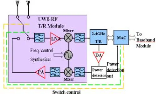
Fig. 1.1 is the first structure draft of UWB RF transceiver system block diagram. As we can see in Fig. 1.1, it uses a broadband frequency synthesizer between 3.3 to 3.6GHz to produce local oscillated signal, and then sends it into the broadband upconvert/downconvert mixer. When it sends to the receiver, it will raise 900 to 1200MHz of receiving signal to 2.4GHz, and then sends it into the 2.4GHz receive/transmit chip. As for the transmitter, it will downconvert the frequency, which is from the 2.4GHz to 900~1200MHz, and then sends it into the power amplifier to enlarge the amplitude and transmits from the antenna.
Figure 1.1 UWB RF transceiver system block diagram.
1.3 Chapter Outline
There are four chapters in this thesis. Chapter one is an introduction. We will talk about the research background first, and introduce the structure and standards of UWB RF transceiver system. Chapter two will include the basic theory of wireless systems and the parameter discussion that needed to be take into consider when receiver and transmitter are independent in the wireless systems. After this, we will
introduce UWB RF T/R module designing procedures and circuit analysis. In chapter three, we will show the fabrication of real circuits and measuring outcome, and have a further discussion according to the outcome. Chapter four will be a conclusion of this thesis.
Chapter2 RF System Theory and Analysis
2.1 Introduction
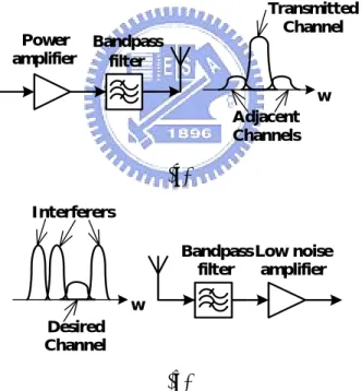
Any wireless system consists of a transmitter and a receiver. The transmitter delivers the carrier signal modulated by information through an antenna. The receiver recovers the information from the received signal from the antenna. Besides, as depicted in Fig. 2.1 [1], the transmitter must employ narrowband modulation, amplification, and filtering to avoid leakage to adjacent channels, and the receiver must be able to process the desired channel while sufficiently rejecting strong neighboring interferers. And, more detail parameters used in transmitter and receiver systems will discuss as follow.
Power amplifier Bandpass filter w Transmitted Channel Adjacent Channels (a) w I nterferers Desired Channel Low noise amplifier Bandpass filter (b)
Figure 2.1 (a) Transmitter and (b) receiver front ends of a wireless transceiver.
2.2 Receiver System Considerations
The input to a wireless transmitter may be voice, video, data, or other
information to be transmitted to one or more distant receivers. So, the basic function of the receiver is to demodulate, or decode, the transmitted baseband data. The performance of the receiver depends on the system design, circuit design, and
working environment. To facilitate the discussion, a basic radio receiver as shown in Fig. 2.2 [2] is used. Data out Demodulator I F filter Mixer Local oscillat or Bandpass filt er Antenna Low noise amplifier amplifierI F
Figure 2.2 Block diagram of a basic radio receiver.
The antenna receives electromagnetic waves radiated from many sources over a relatively broad frequency range. A preselector bandpass filter can minimize the intermodulation and spurious responses by filtering out received signals at undesired frequencies. The bandpass filter is followed by a low noise amplifier, which has a low noise figure, high gain, and high intercept point, can amplify the possibly very weak received signal and minimize the noise power that is added to the received signal. Next, a mixer is used to downconvert the received RF signal to a low frequency signal called intermediate frequency (IF). When IF signal is selected by a IF filter, a high gain IF amplifier raises the power level of the signal so that the baseband information can be recovered easily. This process is called demodulation. A local oscillator provides a LO source which should have low phase noise and sufficient power to pump the mixer. The receiver system considerations are listed below [3]:
1. Sensitivity: Receiver sensitivity quantifies the ability to respond to a weak signal. The requirement is the specified signal-to-noise ratio (SNR) for an analog receiver and bit error rate (BER) for a digital receiver.
2. Selectivity: Receiver selectivity is the ability to reject unwanted signals on adjacent channel frequencies. This specification, ranging from 70 to 90 dB, is difficult to achieve. Most systems do not allow for simultaneously active adjacent channels in the same cable system or the same geographical area.
3. Spurious response rejection: The ability to reject undesirable channel response is important in reducing interference. This can be accomplished by properly choosing the IF and using various filters. Rejection of 70-100 dB is possible. 4. Intermodulation rejection: The receiver has the tendency to generate its own
on-channel interference from one or more RF signals. These interference signals are called intermodulation (IM) products. Greater than 70 dB rejection is normally desirable.
5. Frequency stability: The stability of the LO source is important for low frequency modulated (FM) and phase noise. Stabilized sources using dielectric resonators, phase-locked techniques, or synthesizers are commonly used.
6. Radiation emission: The LO signal could leak through the mixer to the antenna and radiate into free space. This radiation causes interference and needs to be less than a certain level specified by the FCC.
2.2.1 Receiver Noise
In many analog circuits, noise figure is a measure of the degradation in the signal-to-noise ratio between the input and output of the component. The noise figure of a system depends on losses in the circuit, kind of the solid-state device, bias applied, and amplification. The noise figure, F, is defined as
o o i i N S N S output at ratio power noise to Signal input at ratio power noise to Signal F = − − − − =
where Si, Ni are the input signal and noise powers, and So, No are the output signal
and noise power. By definition, the input noise power is assumed to be the noise power resulting from a matched resistor at T0=290K; that is, Ni=kT0B.
Consider Fig. 2.3 [4], which shows noise power Ni and signal power Si being
B, and an equivalent noise temperature Te. If we define Nadded as the noise power
added by the network, then the output noise power can be expressed as
(
Ni Nadded)
G
N0 = + .
The noise figure can be written as
(
)
i added added i i i i N N N N G GS N S F = + + = 1 R networkN oisy R G, B, Te Si Pi= Si+ N i N i= kT0B P0= S0+ N0 T0= 2 9 0 KFigure 2.3 Determining the noise figure of a noisy network.
For a cascaded circuit with n networks as shown in Fig. 2.4, the overall noise figure can be expressed as 1 2 1 1 2 1 3 1 2 1 1 1 − − + + − + − + = n n cas G G G F G G F G F F F … … . F1 G1 F2 G2 Fn Gn F3 G3
…
Figure 2.4 Cascaded noisy circuit with n networks. 2.2.2 Dynamic Range
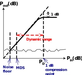
Dynamic range (DR) is generally defined as the ratio of the maximum input level that the circuit can tolerate to the minimum input level at which the circuit provides a reasonable signal quality. The typical definition of DR is shown in Fig. 2.5 [4]. The dynamic range (DR) is defined as the range between the 1dB compression point and the minimum detectable signal (MDS). If the input power is above this range, the output starts to saturate. If the input power is below this range, the noise dominates.
Pout( dB) Pin( dB) 1 dB compression point M DS N oise floor 1 dB PD Dynamic range
Figure 2.5 Illustrating the dynamic range of realistic mixers, amplifiers, or receivers. From the 1dB compression point, gain, bandwidth, and noise figure, the dynamic range (DR) of a receiver can be calculated. Expressing the DR in dBm, we can write as
MDS P
DR= D − .
But, the definition is quantified in different applications differently. Another definition is called the “spurious-free dynamic range” (SFDR). The upper end of the dynamic range is defined as the maximum input level in a two-tone test for which the third-order IM products do not exceed the noise floor. The SFDR is given by
(
P G MDS)
SFDR= OIP3− −
3 2
.
where G is the gain of a receiver, POIP3 is the output power at the third-order, two-tone
intercept point in dBm.
2.2.3 Third-order Intermodulation
When two signals with different frequencies are applied to a nonlinear system, the output in general exhibits some components that are not harmonics of the input frequencies. Called intermodulation (IM), this phenomenon arises from mixing of the two signals when their sum is raised to a power greater than unity. We are particularly interesting in the third-order IM products at 2w1-w2 and 2w2-w1, illustrated in Fig. 2.6
they are difficult to filter from desired channel and may corrupt the desired signal. w w 2 w1-w2 2 w2-w1 w2 w1 w2 w1
Figure 2.6 Intermodulation in a nonlinear system.
The third intercept point (IP3) is a figure of merit for intermodulation product suppression. A high intercept point indicates a high suppression of undesired intermodulation products. Also, it is an important measure of the system linearity. As shown in Fig. 2.7, the magnitude of the IM products grows at three times the rate at which the main signal increases. The third-order intercept point is defined to be at the intersection of the two lines. The horizontal coordinate of this point is called the input IP3 (IIP3), and the vertical coordinate is called the output IP3 (OIP3).
Pin( dB) Pout( dB) M ain signal power I M power O I P3 I I P3
Figure 2.7 Growth of output components in an intermodulation test.
For a cascaded circuit, as shown in Fig. 2.8, the following procedure can be used to calculate the overall system intercept point:
y2( t) x( t) I I P3 ,2 I I P3 ,1 y1( t)
…
yn( t) I I P3 ,nFigure 2.8 Cascaded n nonlinear stages.
dB for dB.
2. Convert intercept point to power (dBm to mW).
3. Assuming all intercept points are independent and uncorrelated, add powers in parallel:
( )
( )
( )
(
mW)
n IP IP IP IP INPUT 3 1 2 3 1 1 3 1 1 3 + + + = … .4. Convert IP3INPUT from power (mW) to dBm.
2.3 Transmitter System Considerations
The basic function of the transmitter is to modulate, or encode, the baseband information onto a high frequency sine wave carrier signal that can be radiated by the transmit antenna. The reason for this is that signals at higher frequency can be radiated more effectively, and use the RF spectrum more efficiently, than the direct radiation of the baseband signal. A simple transmitter could have only an oscillator, and a complicated one would include a phase-locked oscillator or synthesizer. Generally, a transmitter consists of a modulator, an oscillator, an upconverter, filters, and power amplifiers as shown in Fig. 2.9 [2].
Data in
Modulator I F filter Mixer
Local oscillator Bandpass filter Antenna Power amplifier
Figure 2.9 Block diagram of a basic radio transmitter.
First, the baseband data modulates an intermediate sine wave signal, then the IF signal upconverts to the desired RF transmit frequency using a mixer. A bandpass filter allows the RF signal to pass, while rejecting the spurious interferers. A power amplifier is used to increase the output power of the transmitter. Finally, the antenna radiates a propagating electromagnetic wave converted from the modulated carrier
signal. The transmitter system considerations are listed below [3]:
1. Power output and operating frequency: The output RF power level generated by a transmitter at a certain frequency or frequency range.
2. Efficiency: The dc-to-RF conversion efficiency of the transmitter. Efficiency is defined as =( )×100%
dc RF
P P
η . For a power amplifier, the power added
efficiency (PAE) is defined as = − ×100%
dc in out P P P
η where Pout and Pin are the
output and °input RF power, respectively.
3. Power output variation: The output power level variation over the frequency range of operation.
4. Frequency tuning range: The frequency tuning range due to mechanical or electronic tuning.
5. Stability: The ability of an oscillator/transmitter to return to the original operating point after experiencing a slight electrical or mechanical disturbance.
6. Circuit quality (Q) factor: The loaded and unloaded Q-factor of the oscillator’s resonant circuit.
7. Noise: The AM, FM, and phase noise. AM noise is the unwanted amplitude variation of the output signal, FM noise is the unwanted frequency variations, and phase noise is the unwanted phase variations.
8. Frequency variations: Frequency jumping, pulling, and pushing. Frequency jumping is a discontinuous change in oscillator frequency due to nonlinearities in the device impedance. Frequency pulling is the change in oscillator frequency versus a specified load mismatch over 360° of phase variation. Frequency pushing is the change in oscillator frequency versus dc bias point variation. 9. Post-tuning drift: Frequency and power drift of a steady-state oscillator due to
10. Spurious signals: Output signals at frequencies other than the desired oscillation carrier.
11. Adjacent channel power ratio (ACPR): A figure-of-merit to evaluate the intermodulation distortion performance of power amplifiers designed for digital wireless communication systems.
2.3.1 Transmitter Noise
In RF systems, local oscillators provide the carrier signal for both the receiver and transmit paths. If the LO output contains phase noise, both downconverted and upconverted signals are corrupted. So, it is important to concern about the noise of the local oscillators. Consider the output power shown in Fig. 2.10 [3], for an ideal sinusoidal oscillator operating at f0, the spectrum assumes the shape of an impulse.
But, for an actual oscillator, the spectrum exhibits “skirts” around the carrier frequency. f Ou tp u t p o w e r f Ou tp u t p o w e r f0 f0
I deal signal N oise signal
Figure 2.10 Ideal signal and noisy signal.
As shown in Fig. 2.11, L(fm) is the difference of power between the carrier at f0
and the noise at fm. It is a ratio of single-sideband noise power normalized in 1Hz
bandwidth to the carrier power and is defined as
( )
C N power signal Carrier carrier from offset f at bandwidth Hz in power Noise f L m m = = 1 . The power is plotted in dB scale. The unit of L(fm) is dBc/Hz.Ou tp u t p o w e r (d B ) f0 f C N L( fm) f0+ fm
Figure 2.11 Oscillator output power spectrum. 2.3.2 Adjacent Channel Power Ratio
Adjacent Channel Power Ratio (ACPR) is normally used a figure of merit for power amplifiers to characterize their linearity. ACPR is a measure of spectral regrowth, appears in the signal sidebands, and is analogous to IM3/IM5 for an analog RF amplifier. Fig. 2.12 [1] shows the power measurement frequency spectrum. And, the ACPR is defined as
channel offset the in density spectral Power channel main the in density spectral Power ACPR= and is expressed in dBc. Signal Channel Adjacent Channel
w
Figure 2.12 Adjacent channel power.2.4 Analysis of the System
2.4.1 Frequency Conversion
First, before we design this RF T/R module, we need to decide the working frequency of whole system. We already know that transmit/receive signals are between 900MHz and 1200MHz, and use 2.4GHz of 802.11b as baseband module
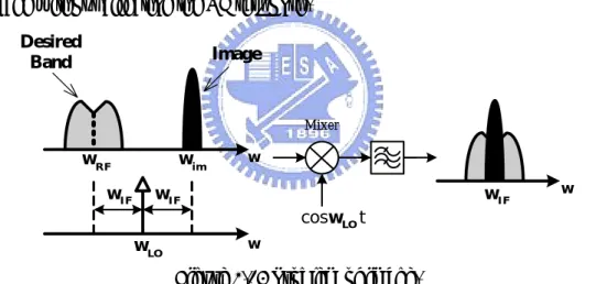
signal; so the main factor of following is to consider how to set up LO frequency. As shown in Fig. 2.13, the problem of image is a serious one which we will take into account. The radio frequency (RF) input signals at frequency of (wLO + wIF) and
(wLO - wIF) will be downconverted to the same intermediate frequency (IF) wIF by
mixing them with a local oscillator at frequency of wLO. The image interferer must be
rejected to prevent aliasing with the desired signal. In addition, to ensure that the image frequency is outside the RF bandwidth of the receiver, it is necessary to have
2
RF IF
B
f > ,
where BRF is the RF bandwidth of the receiver. The separation between the RF and
image frequencies must be greater than the bandwidth of the system in order to filter the image without affecting the RF response.
Mixer w w wLO wI F wI F wim wRF Desired Band Image w wI F coswLOt
Figure 2.13 Problem of image.
Finally, because of considering the cost and system structure simplified, we choose a voltage controlled oscillator between 3.3GHz and 3.6GHz as our LO frequency. 2 2 9 . 0 2 . 1 4 . 2 RF IF B GHz GHz GHz f = > − =
From this formula, we could know that if we choose LO frequency this way, image frequency would not act within the wanted bandwidth. Because of above reason, a band select filter between receiver and antenna is essential to pass the desired signal and reject the interferences.
2.4.2 Stages Tracking
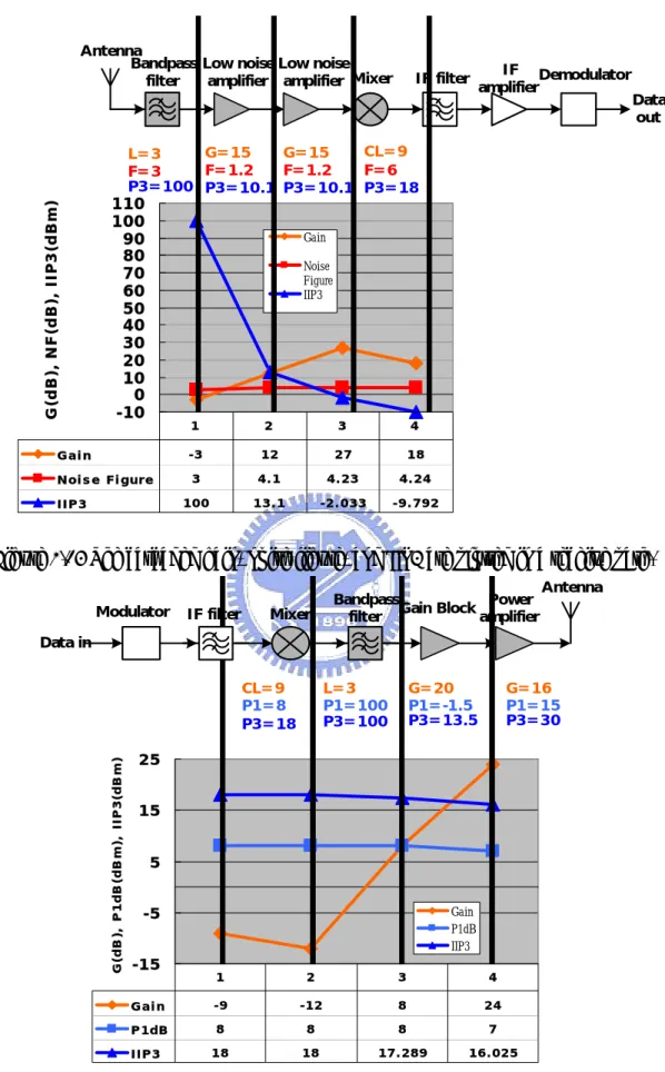
The receiver encounters two types of the noise: the noise picked up by the antenna and the noise generated by the receiver. And, the noise that occurs in a receiver masks weak signals and limits the ultimate sensitivity of the receiver. So, consider the gain, noise figure, and third-order intercept point listed for each component in Fig. 2.14, which is the typical value of the chip data sheet. Using the cascade formulas for noise figure and third-order intercept, the gain, noise figure, and third-order intercept are plotted in Fig. 2.14 at the output of each stage, versus position through the receiver.
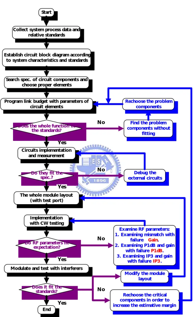
The specifications for a transmitter depend on the applications. For communication systems, low noise and good stability are required. As discussed in previous sections, the power level that exceed the 1 dB compression point P1 of an amplifier will cause harmonic distortion, and power levels in excess of the third-order intercept point P3 will cause intermodulation distortion. Thus it is important to track P1 and P3 through the stages of the transmit path as shown in Fig. 2.15.
-100 10 20 30 40 50 60 70 80 90 100 110 G (d B ), N F (d B ), IIP 3 (d B m) Gain Noise Figure IIP3 Gain -3 12 27 18 Noise Figure 3 4.1 4.23 4.24 IIP3 100 13.1 -2.033 -9.792 1 2 3 4 Data out Demodulator I F filter Mixer Bandpass filter Antenna Low noise amplifier amplifierI F L= 3 P3 = 1 0 0 G= 1 5 P3 = 1 0 .1 Low noise amplifier CL= 9 P3 = 1 8 G= 1 5 P3 = 1 0 .1 F= 3 F= 1 .2 F= 1 .2 F= 6
Figure 2.14 The cascaded gain, noise figure, and IIP3 are plotted in a receive path.
-15 -5 5 15 25 G(d B ), P 1 d B (d B m ), IIP 3 (d B m ) Gain P1dB IIP3 Gain -9 -12 8 24 P1dB 8 8 8 7 IIP3 18 18 17.289 16.025 1 2 3 4 Data in
Modulator I F filter Mixer Bandpassfilter
Antenna Power amplifier G= 1 6 P1 = 1 5 P3 = 3 0 L= 3 P1 = 1 0 0 P3 = 1 0 0 Gain Block G= 2 0 P1 = -1 .5 P3 = 1 3 .5 CL= 9 P1 = 8 P3 = 1 8
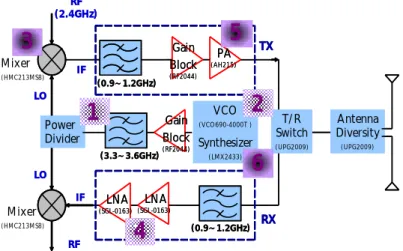
2.4.3 Practical Design M ix er ( HM C2 1 3 M S8 ) M ix er ( HM C2 1 3 M S8 ) LN A ( SGL-0 1 6 3 ) PA ( A H2 1 5 ) Gain Block ( RF2 0 4 4 ) A nt enna Diver sit y ( U PG2 0 0 9 ) TX RX RF ( 2 . 4 GH z) RF ( 2 . 4 GH z) LO LO I F I F Power Divider VCO ( VCO 6 9 0 -4 0 0 0 T ) Synt hesizer ( LM X2 4 3 3 ) Gain Block ( RF2 0 4 4 ) ( 0 .9 ~ 1 .2 GHz) ( 3 .3 ~ 3 .6 GHz) ( 0 .9 ~ 1 .2 GHz) T/ R Swit ch ( U PG2 0 0 9 ) LN A ( SGL-0 1 6 3 ) M ix er ( HM C2 1 3 M S8 ) M ix er ( HM C2 1 3 M S8 ) LN A ( SGL-0 1 6 3 ) PA ( A H2 1 5 ) Gain Block ( RF2 0 4 4 ) A nt enna Diver sit y ( U PG2 0 0 9 ) TX RX RF ( 2 . 4 GH z) RF ( 2 . 4 GH z) LO LO I F I F Power Divider VCO ( VCO 6 9 0 -4 0 0 0 T ) Synt hesizer ( LM X2 4 3 3 ) Gain Block ( RF2 0 4 4 ) ( 0 .9 ~ 1 .2 GHz) ( 3 .3 ~ 3 .6 GHz) ( 0 .9 ~ 1 .2 GHz) T/ R Swit ch ( U PG2 0 0 9 ) LN A ( SGL-0 1 6 3 )
Figure 2.16 Block diagram of the RF transceiver.
The block diagram of Fig. 2.16 shows the proposed RF transceiver module. It is a half-duplex system, where the transmitter and receiver are not operating simultaneously, and duplexing can be achieved with a T/R switch. A single-pole double-throw switch can connect the antenna to either the transmitter or the receiver. In transmitting path, we need to connect a bandpass filter after mixer to restrain the intermodulation products, which is producing at mixer, and then connect it with a gain block and a power amplifier to increase transmit power to reach requiring 30dBm. In receiving path, signal from antenna need to be filtered by a band select bandpass filter, which is chosen in-band signal and weaken out-of-band signal. In the LO path, in order to increase stability of VCO, we need to add a synthesizer circuit to make it oscillate stably. Next, in order to increase transmitting power for driving mixer, one more gain block is required. Besides, a bandpass filter to restrain the harmonic signal of VCO is also needed.
Finally, for a complete T/R module, except to have proper control of the entirety functions, the jams and matching problems between circuits need also be overcome. Whether circuit layout is suitable or not is another key point. We need to avoid coupling between signals, and we also hope to reduce the size of circuit; each one
connects to others. So, we could say that this planning process is very complicated. As a result, we bring up an effective design flow chart as shown in Fig. 2.17 as a guideline for designing of our RF T/R module. When there are some functions of whole module do not meet the specs, we need to re-select some of those key components.
Circuit s implement at ion and measurement
The whole module layout ( wit h t est port )
Do t hey fit t he spec.?
Program link budget wit h paramet ers of circuit element s
Search spec. of circuit component s and choose proper element s
Est ablish circuit block diagram according t o syst em charact erist ics and st andards
Collect syst em process dat a and relat ive st andards
St art
Implement at ion wit h CW t est ing
M odulat e and t est wit h int erferers
Do RF paramet ers fit expect at ion? Does it fit t he st andards? End Rechoose t he problem component s Find t he problem component s wit hout
fit t ing
Debug t he ext ernal circuit s
M odify t he module layout
Rechoose t he crit ical component s in order t o increase t he est imat ive margin
Yes N o Yes N o Yes N o Yes N o
Examine RF paramet ers: 1. Examining mismat ch wit h
failure .
2. Examining P1dB and gain wit h failure . 3. Examining IP3 and gain
wit h failure .
Does t he whole funct ion fit t he st andards?
Gain P1dB
IP3
Chapter3 Implementation and
Measurement
3.1 Introduction M ix er ( HM C2 1 3 M S8 ) M ix er ( HM C2 1 3 M S8 ) LN A ( SGL-0 1 6 3 ) PA ( AH2 1 5 ) Gain Block ( RF2 0 4 4 ) Ant enna Diversit y ( UPG2 0 0 9 ) TX RX RF ( 2.4 GHz) RF ( 2.4 GHz) LO LO I F I F Power Divider VCO ( VCO 6 9 0 -4 0 0 0 T ) Synt hesizer ( LM X2 4 3 3 ) Gain Block ( RF2 0 4 4 ) ( 0 .9 ~ 1 .2GHz) ( 3 .3 ~ 3 .6GHz) ( 0 .9 ~ 1 .2GHz) T/ R Swit ch ( UPG2 0 0 9 ) LN A ( SGL-0 1 6 3 ) M ix er ( HM C2 1 3 M S8 ) M ix er ( HM C2 1 3 M S8 ) LN A ( SGL-0 1 6 3 ) PA ( AH2 1 5 ) Gain Block ( RF2 0 4 4 ) Ant enna Diversit y ( UPG2 0 0 9 ) TX RX RF ( 2.4 GHz) RF ( 2.4 GHz) LO LO I F I F Power Divider VCO ( VCO 6 9 0 -4 0 0 0 T ) Synt hesizer ( LM X2 4 3 3 ) Gain Block ( RF2 0 4 4 ) ( 0 .9 ~ 1 .2GHz) ( 3 .3 ~ 3 .6GHz) ( 0 .9 ~ 1 .2GHz) T/ R Swit ch ( UPG2 0 0 9 ) LN A ( SGL-0 1 6 3 )1
2
3
5
6
4
Figure 3.1 Block diagram of the RF transceiver.
Through the system budget calculated in previous chapter, the whole system with appropriate ICs is shown in Fig. 3.1. The main purpose of this chapter is to describe each individual circuit such as filter, VCO, mixer, LNA, PA, and synthesizer and its measured results. The last thing is to estimate whole transceiver module, and discuss the possible reasons of some of these results that are not as we expected.
3.2 RF Bandpass Filters
Filters are key components in all wireless transmitters and receivers. They are used to reject interfering signals outside the operating band of receivers and transmitters. Important filter parameters include the cutoff frequency, insertion loss, and the out-of-band attenuation rate, measured in dB per decade of frequency. Filters with sharper cutoff responses provide more rejection of out-of-band signals.
3.2.1 3.3~3.6 GHz Bandpass Filter
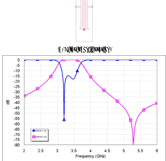
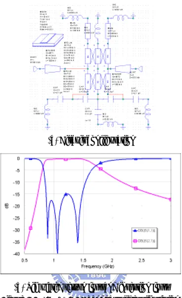
According to the system structure, we know that a 3.3~3.6GHz is required to pass the desired LO signal and reject the harmonic signals. Following shows the filter
layout, which is designed by a 3-D EM simulator Sonet. The filter is designed with a center frequency of 3.45GHz, bandwidth of 300MHz. The filter size is 244Χ470mil. The passband insertion loss is expected to be within -1dB and the return loss to be better than -10dB.
(a) Circuit configuration.
(b) Simulated return loss and insertion loss. Figure 3.2 3.3~3.6 GHz bandpass filter simulation.
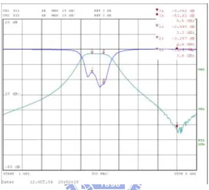
Fig. 3.3 shows the photograph of the filter and its measured results. The filter is an interdigital filter with three quarter-wave resonators. The measured passband insertion loss is within -3.2dB and the return loss is better than -10dB.
(a) Circuit layout.
(b) Measured return loss and insertion loss.
Figure 3.3 3.3~3.6 GHz bandpass filter physical implementation. 3.2.2 0.9~1.2 GHz Bandpass Filter
In the transmitting and receiving paths, we need a 0.9~1.2GHz bandpass filter. The filter we proposed is a three-resonator combline filter. Figure 3.4 depicts the schematic circuit and the simulated results where the circuit simulator is AWR’s Microwave Office. The filter is designed with center frequency of 1.05GHz, and bandwidth of 300MHz. The size of circuit is 330Χ515mil. The passband insertion loss is expected to be within -1dB and the return loss to be better than -10dB.
(a) Circuit configuration
(b) Simulated return loss and insertion loss. Figure 3.4 0.9~1.2 GHz bandpass filter simulation.
Figure 3.5 shows the circuit photo and measured results of the proposed filter. It can be seen in Fig. 3.5(a) that there are two coupling capacitors to enhance the coupling between resonators. The capacitance value is 3.3pF for both capacitors. The measured passband insertion loss is within –2.7dB and the return loss is better than -20dB..
(a) Circuit layout.
(b) Measured return loss and insertion loss.
Figure 3.5 0.9~1.2 GHz bandpass filter physical implementation.
3.3 Broadband Voltage Controlled Oscillator (VCO)
Oscillators are required in wireless receivers and transmitters to provide frequency conversion, and to provide sinusoidal sources for modulation. Usually, these sources need to be tunable over a frequency range, and must provide very accurate output frequencies. Frequency can be tuned by adjusting the value of the LC network, perhaps electronically with a varactor diode.
We choose Sirenza VCO690-4000T to be our broadband VCO, and change capacitance value to make it oscillate in the wanted frequency range. A dc voltage of 5 volts, and controlling voltage of 0 volts to 2.5 volts is desired. Fig. 3.6 is the real circuit photograph of the VCO. Figure 3.7 depicts the tuning voltage Vt versus oscillating frequency, which is measured by maximum hold mode of spectrum analyzer. It is shown in this figure that when control voltage increases slowly, the oscillated frequency will also increase from 3.28GHz to 3.67GHz.
Figure 3.6 Photograph of broadband voltage controlled oscillator.
Figure 3.7 Controlled voltage tuning range.
Next, it is to measure the phase noise of the VCO. The phase noise is measured at frequency 2MHz.1MHz, and 500KHz offset from center frequency respectively. It can be seen in Fig. 3.8 that they are all over 100dBc/Hz.
Phase noise = -79.73 dBm-10logRBW= -129.73 dBc/Hz
(a) @ 2 MHz offset.
Phase noise = -66.94 dBm-10logRBW= -116.94 dBc/Hz
Phase noise = -61.52 dBm-10logRBW= -111.52 dBc/Hz
(c) @ 500 kHz offset. Figure 3.8 Measured phase noise.
Finally, the second harmonic signal is measured to be –16.96dBc from its fundamental signal. This can be largely improved by the LO filter described previously.
Figure 3.9 Measured power of 2-order harmonic frequency.
3.4 Broadband Mixer
The primary function of a mixer in a communication system is to translate signal from one frequency (RF frequency) to another frequency (IF frequency). A passive mixer always produces an output signal (IF) of less power than the input signal (IF).
This loss is characterized by the mixer conversion loss. Mixers that use active components generally have lower conversion loss, and may even have conversion gain. As in the case of amplifiers, harmonic distortion and noise are also important considerations in mixer performance.
Fig. 3.10 shows the photograph of the broadband mixer. We choose HMC213MS8 of Hittite as our mixer. It operates with LO frequency of 3.3 to 3.6GHz, IF frequency of 2.4 to 2.5 GHz, and RF frequency of 900 to 1200MHz.
Figure 3.10 Photograph of broadband mixer.
Fig. 3.11 shows measured mixer conversion loss versus LO input power where the IF frequency is 2.4GHz and with –10dBm of power. From this graph we could see obviously that the conversion loss is better than 10dB as LO power over 10dBm. Fig. 3.12 and 3.13 shows the measured mixer conversion loss versus LO frequency where the IF frequencies are 2.4GHz and 2.5GHz respectively. The IF input power is from –5 to –13dBm as depicted with different curves in Fig. 3.12 and 3.13.
Figure 3.12 Conversion loss V.S. LO freq. @ IF= 2.4 GHz, -10 dBm.
Figure 3.13 Conversion loss V.S. LO freq. @ IF=2.5 GHz, -10 dBm.
Fig. 3.14 depicts the measured IF to RF isolation of the mixer with IF power of –10dBm. The isolation is better than –29dBm. Fig. 3.15 shows the leakage of IF power to the RF port versus input IF power where the IF frequency is fixed at 2.4GHz. According to this measured results, we need to further decrease the leakage IF signal to an appropriate degree.
Figure 3.14 IF to RF isolation @ IF= -10 dBm.
Figure 3.15 Different power of IF to RF leakage @ IF= 2.4 GHz.
3.5 Broadband Low Noise Amplifier
A low noise amplifier is used in the input stage of a receiver. This is most critical in the front end of a receiver, where the input signal level is very small, and it is desired to minimize the noise added by the receiver circuitry. In addition, the noise power in a receiver is affected more by the first few components than by later components. Thus it is important that the first amplifier in a receiver have as low a noise figure as possible.
We choose Sirenza SGL-0169 as the low noise amplifier. According to the data sheet, we adjust the input and output capacitances to make it work in the desired 0.9GHz to 1.2GHz frequency band. Fig. 3.16 depicts the photograph of the LNA..
Figure 3.16 Photograph of broadband low noise amplifier.
Fig. 3.17 shows the measured gain and return loss of this LNA. The frequency between dotted lines is the desired frequency band, 0.9GHz~1.2GHz. Within this area, the insertion gain is beyond 17.54dB, and return loss is better than –13.58dB. The measured noise figure and gain is shown in Fig. 3.18. it can be found in this figure that the measured noise figure is 1.77 to 1.65 dB with associated gain of 19.66dB to 17.54dB.
Figure 3.17 Measured S-parameters of broadband low noise amplifier.
Figure 3.18 Measured noise figure of broadband low noise amplifier.
Power amplifiers are used in the final stages of wireless transmitters to increase the radiated power level. So, high linearity is an important parameter for power amplifier. Because transistors are nonlinear devices, transistor amplifier exhibit two nonlinear effects: saturation and harmonic distortion. On the other hand, important considerations for power amplifiers are efficiency, gain, and intermodulation effects.
We choose WJ AH215 as our power amplifier. The DC biase voltage is 5 volts. Appropriated changing of the matching capacitances at input and output are required to fit this PA to work in the desired frequency band. After adjusting, we could have maximal output gain. Following is the circuit photograph.
Figure 3.19 Photograph of broadband power amplifier.
After adjusting a little bit of power amplifier circuit, we measure its small signal S-parameters. As it is shown in Fig. 3.20 that the measured gain is higher than 13dB and the measured return loss is better than –8dB. In order to insure the output power reaches 30dBm, we execute PldB measurement. As we can see in Fig. 3.21, when input
Figure 3.20 Measured S-parameters of broadband power amplifier.
Figure 3.21 Measured P1dB of broadband power amplifier.
3.7 Frequency Synthesizer
Frequency synthesizers consist of phase-locked loops and other circuits that provide accurate, stable, and tunable frequency outputs. Important parameters that characterize frequency synthesizers are tuning range, frequency switching time, frequency resolution, cost, and power consumption. Another very important parameter is the noise associated with the output spectrum of the synthesizer, in particular the
phase noise.
We choose NS LMX2433 as our frequency synthesizer IC. Fig. 3.22 is the picture of circuit layout, where the Vcc is worked at 5 volts, and input DSP signal pins are located at place marked with “1” to control this frequency synthesizer. Use PLL to lock the VCO with a reference crystal oscillator and the output frequency should cover 3.3~3.6GHz. A DSP control program “Codeloader” is used here, which is free from download at National Semiconductor website. Fig. 3.23 is interface of Codeloader. Before starting to use it, we need to set up frequency synthesizer type LMX2433, and choose RF PLL manual. Inside the RF PLL manual, input wanted value at Counter field in PLL to decide the distance of each frequency jumping. Or input the frequency that we want to lock it at VCO field directly. In the following, we will introduce each special character of input waveform at spectrum analyzer.
Figure 3.23 Codeloader interface.
Location marked by “2” in Fig. 3.22 is the output port of the frequency synthesizer. Fig. 3.24 shows the measured tuning range corresponding to VCO’s control voltage. If we want to generate LO frequency include 3.3GHz~3.6GHz, the control voltage Vt needs to be within 0.5 to 2.5 volts. The next step is to observe the phase noise of synthesized signal at frequency 3.3GHz, 3.4GHz, and 3.6GHz respectively. The measured results are shown in Fig. 3.25. We measure the phase noise at 500KHz offset from carrier frequency. The measured phase noises are all better than –109dBc/Hz @500kHz offset.
Phase noise = -60.93 dBm-10logRBW= -110.93 dBc/Hz
(a) @ 3.3 GHz.
Phase noise = -59.97 dBm-10logRBW= -109.97 dBc/Hz
Phase noise = -60.33 dBm-10logRBW= -110.33 dBc/Hz
(c) @ 3.6 GHz.
Figure 3.25 Measured phase noise at 500 kHz offset.
Location marked with “3” in Fig. 3.22 is the output where the signal is amplified and filtered to have the LO signal with proper power and clean from harmonic and spur signals. The signal is measured again with different frequencies of 3.3GHz, 3.4GHz, and 3.6GHz. Fig. 3.26(a) shows the measured spectrum of 3.3GHz signalwhere the frequency span is 1MHz. The phase noise at 100KHz offset is calculated to be –104.87dBc/Hz, and transmit power is 9.39dBm.
Phase noise = -64.87 dBm-10logRBW= -104.87dBc/Hz @ 100kHz offset. Fig. 3.26(b) and (c) shows the measured spur and harmonic signals. The results shows that the second harmonic signal is –65.29dBc where the third harmonic signal is –70.15dBc, and no apparent spur signals can be found.
Phase noise = -64.87 dBm-10logRBW= -104.87 dBc/Hz
(a) Phase noise with 100 kHz offset.
(c) 3-order harmonic power spectrum. Figure 3.26 Measured power spectrum at 3.3 GHz.
Fig. 3.27(a) is the measured results at 3.4GHz. The measured phase noise is –106.14dBc/Hz at 100KHz offset, and output power is 8.86dBm.
Phase noise = -66.14dBm-10logRBW= -106.14dBc/Hz @100kHz offset. Fig. 3.27(b) and (c) shows the measured spur and harmonic signals. The results shows that the second harmonic signal is –65.29dBc where the third harmonic signal is –70.15dBc, and no apparent spur signals can be found.
Phase noise = -66.14 dBm-10logRBW= -106.14 dBc/Hz
(a) Phase noise with 100 kHz offset.
(c) 3-order harmonic power spectrum. Figure 3.27 Measured power spectrum at 3.4 GHz.
Fig. 3.28(a) is the measured results at 3.4GHz. The measured phase noise is –102.82dBc/Hz at 100KHz offset, and output power is 6.39dBm.
Phase noise = -62.82dBm-10logRBW= -102.82dBc/Hz @ 100kHz offset. Fig. 3.28(b) and (c) shows the measured spur and harmonic signals. The results shows that the second harmonic signal is –50.86dBc where the third harmonic signal is –53.05dBc, and no apparent spur signals can be found.
Phase noise = -62.82 dBm-10logRBW= -102.82 dBc/Hz
(b) 2-order harmonic power spectrum.
(c) 3-order harmonic power spectrum. Figure 3.28 Measured power spectrum at 3.6 GHz.
3.8 Measurement and Discussion
Fig. 3.29 is the whole RF transceiver module after integrating all of above described circuits. The whole project is planed to finish within three years. In Fig. 3.29, the two of right-hand side connectors need to be connected with antenna module. Two connectors located at center of the board are 2.4GHz IF signal input and output ports respectively. The module has many dc and logic pins needs to be connected with baseband module. There are no special requirements and limitation about RF T/R module, except the operating frequency and bandwidth and transmitted signal power is controllable and can reach at least 30dBm. And, because there are some difficulties in obtaining appropriate measuring equipments, we could only measure some simple parameters, such as small signal gain, output power, and frequency spectrum to fit them into practical situation. We need to find possible components that may have bad influence on over all module performances. The following is the discussion of transmit path and receive path.
3.8.1 Transmit Path
Figure 3.30 Photograph of transmit path.
Fig. 3.30 is a circuit layout of transmit path. Thr RF signal is sent from input port and passes through a bandpass filter, Gain Block, power amplifier, and then goes to the output port. The DC bias voltage is five volts, and an extra DC power switch is added to switch off the power amplifier during receiving mode for energy saving. The baseband module will control this DC power switch in the future. Fig. 3.31 is the measured small signal S-parameters of the whole transmitter module. The approximate filter response curve can be found in the figure. The in-band small signal gain is over 30dB. It is enough to amplify the modulated RF signal which we want to transmit. Spect rum Analyzer 802.11b PC T/ R M odule Test Cable USB Test Cable + 5V
Figure 3.32 Transmit testing setup diagram.
We already know that IF frequency is 2.4GHz. So, we use a 802.11b WLAN card to generate 2.4GHz CDMA IF signal and after down converting to RF frequency the signal is send to the transmitter. The transmitter outputs are directly sent to a spectrum analyzer. Fig. 3.32 depicts the transmitter test setup. Shown in Fig. 3.33(a) and (b) are the output spectrums. Fig. 3.33(a) shows transmitted carrier only and the output power is 28dBm. Fig. 3.33(b) shows spectrum of a transmitted packet. There are some adjacent channel power is generated as shown in Fig. 3.33(b). These adjacent channel power rejection decreases as the output power increases.
(a) Power spectrum of transmitted carrier.
(b) Power spectrum of transmitted packets. Figure 3.33 Transmit testing on spectrum analyzer. 3.8.2 Receive Path
Figure 3.35 Measured S-parameters of receive path.
Fig. 3.34 is a receive circuit layout. The receiver gets signal from antenna. The received signal goes through a bandpass filter to select appropriate frequency and the signal is then amplified by a two-stage LNA. The bias voltage is also five volts. Fig. 3.35 shows the measured S-parameters of the receiver. The in-band small signal gain is over 30dB, and it is enough to amplify the received signal to proper level..
802.11b PC T/ R M odule Test Cable USB Test Cable 802.11b PC T/ R odule USB Test Cable -50 dB + 5V M + 5V
Figure 3.36 Receive testing setup diagram.
Figure 3.36 depicts the setup for the receiver testing. A 802.11b card together with the transmitter described above is used to transmit the CDMA signal. The connection between receiver and transmitter is a high loss test cable to simulate the wireless environment. As shown in Fig. 3.37, we use a test software, which is downloaded from website, to test the receiver. When we set transmitted signal to be 2Mbps, we get some BER of the received signal. It is possibly due to phase noise, and spurious caused by nonlinearities of circuit.
Figure 3.37 The diagnostic program (MFP) interface. 3.8.3 Measurements Baseband Baseband I F( 2 .4 GHz) RF( 0 .9 ~ 1 .2 GHz) LO ( 3 .3 ~ 3 .6 GHz) DSP control PA O N / O FF & T/ R switch LN A O N / O FF TX RX I F( 2 .4 GHz) 5 volts 4 5 0 mA 28 dBm 46 .9 1 m m 1 3 6 .3 3 mm
Figure 3.38 Photograph of transceiver module.
Fig. 3.38 shows the complete RF T/R module. The specifications are described as following. The LO frequency is between 3.3GHz and 3.6GHz, IF frequency is 2.4GHz, and RF frequency is between 0.9GHz and 1.2GHz. The measured output power is 28dBm, the size is 46.91mmΧ136.33mm, and relative bandwidth is 28.57%.
BPF Return Loss(dB) Insertion Loss(dB) 3.3~3.6GHz < -15 -2.94 ~ -3.257
VCO (Sirenza VCO690-4000T)
Tuning Range Phase Noise (2MHz offset) Phase Noise (1MHz offset) Phase Noise (500kHz offset) 3.28~3.67GHz (0~2.5V) -129.73 dBc/Hz -116.94 dBc/Hz -111.52 dBc/Hz Mixer (Hittite HMC213MS8) Conversion Loss (LO=10dBm) IF to RF leakage @ IF=-10dBm 10 < -29 dB LNA (Sirenza SGL-0169)
Return Loss (dB) Insertion Loss (dB)
Noise Figure
900MHz -13.58 19.96 1.66
1200MHz -16.82 17.84 1.72
PA (WJ AH215) Return Loss (dB) Insertion Loss
(dB) P1dB (dBm) 900MHz -7.99 13.334 > 31 1200MHz -8.525 13.323 Synthesizer (NS LMX2433) Tuning Range 3.3 ~ 3.6GHz (0.5~2.5V) Phase Noise (500kHz offset) 2nd-order harmonic suppression 3rd-order harmonic suppression 3.3GHz -104.87 dBc/Hz -65.29 dB -70.15 dB 3.4GHz -106.14 dBc/Hz -57.41 dB -52.13 dB 3.6GHz -102.82 dBc/Hz -50.86 dB -53.09 dB
Ch4 Conclusion
In the future, this module will combine with baseband module and antenna module. And, in order to make the performance better, the RF T/R module still have room to be improved. Some suggestions are listed as following.
1. Load-pull Measurements of the PA: We can measure the source-pull and load-pull data of the PA. Then, these data helps us to design the matching networks for power amplifiers to achieve maximum power, better PAE, and good IM3 and ACPR.
2. Insertion Loss of the Filter: On the receiving path, a preselect filter is placed in fromt of LNA. So, in order to have lower receiver noise figure, the loss of the bandpass filter should be as low as possible. Furthermore, on the transmit path, the filter may also reduce the spurious and harmonic content of the output signal.
3. LO power: Because the conversion loss of mixer decreases as LO power decreases. Proper LO power level that saturates the loss of the mixer is essential. We can increase the LO power by changing of gain block chip.
4. Size of the Whole Module: To make the whole module more compact, we can change all passive components in LTCC. Reducing of test and ground pad can also reduce the module size. Rough estimation shows that a 50% of size reduction would be possible.
In conclusion, the RF T/R module is important and commonly used unit in general wireless systems. Wider bandwidth and smaller size are always in demand. The results of this thesis can be applied to other wireless systems.
References
[1] Behzad Razavi, RF Microelectronics, Prentice Hall PTR.
[2] David M. Pozar, Microwave and RF Wireless Systems, John Wiley & Sons, N. Y. 1998.
[3] Kai Chang, Inder Bahl, and Vijay Nair, RF and Microwave Circuit Component
Design for Wireless Systems, John Wiley & Sons, INC.
[4] David M. Pozar, Microwave Engineering, 2nd Edition, John Wiley & Sons, N. Y. 1998.