INTRODUCTION
The eutectic In49Sn solder possesses the advan-tages of higher ductility, better wettability, and longer fatigue life, merits suitable for the employment of In49Sn as a candidate for Pb-free solders in the elec-tronics industry. On account of its low melting point, this eutectic solder has also been commonly used for bonding recycled-sputtering targets to their Cu back plates. During the soldering process, intermetallic compounds are formed at the In-49Sn/Cu interfaces, providing evidence of the interfacial reactions and connections between In-49Sn solders and Cu plates. However, too thick an intermetallic compound can re-sult in brittle cracking at the interfaces. Therefore, phase identification and growth analysis of the re-acted intermetallics during interfacial reactions be-tween In-49Sn solders and Cu substrates provide vital links in such an application.
The interfacial reactions between eutectic In-Sn solders and Cu substrates have been studied.1–7 Roming et al.1dipped Cu into In-50Sn molten solder and then aged the specimens in air at the
tempera-tures ranging from 60°C to 110°C. Two intermetallic compounds of Cu2(Sn,In) and Cu2In3Sn were found at the In-Sn/Cu interface. According to their report, the intermetallic growth was dominated by Cu2In3Sn, while the Cu2(Sn,In) phase was formed as the initial layer at the interface during the dipping process but failed to attain any further growth. The rate-limiting mechanism for the growth of the inter-metallic layer changed with temperature. At higher temperatures, the intermetallic growth was limited by volume diffusion, while at lower temperatures, the growth kinetics was interfacial controlled. Vianco et al.2investigated the solid-state reactions between Cu and four solders (pure In, In-50Sn, pure Sn, and Pb-63Sn). They found that the intermetallic layer formed at the In-50Sn/Cu interface was more irregular than in the other three cases. In the case of In-50Sn/Cu interfacial reactions, the intermetallic compounds contained a thin Cu17Sn9In24layer near the solder matrix and a thicker Cu26Sn13In8layer on the side of the Cu substrate. In a study on the inter-facial reactions and mechanical behaviors of solder joints on Cu substrates, Frear and Vianco3 found that In-50Sn/Cu exhibited faster intermetallic
Phase Identification and Growth Kinetics of the Intermetallic
Compounds Formed during In-49Sn/Cu Soldering Reactions
T.H. CHUANG, C.L. YU, S.Y. CHANG, and S.S. WANG
Department of Materials Science and Engineering, National Taiwan University, Taipei 106, Taiwan For the application of In-49Sn solder in bonding recycled-sputtering targets to Cu back plates, the intermetallic compounds formed at the In-49Sn/Cu inter-face are investigated. Scanning electron microscopy (SEM) observations show that the interfacial intermetallics consist of a planar layer preceded by an elongated scalloped structure. Electron-probe microanalyzer analyses indicate that the chemical compositions of the planar layer and the scalloped structure are Cu74.8In12.2Sn13.0 and Cu56.2In20.1Sn23.7, respectively, which correspond to the ε-Cu3(In,Sn) and -Cu6(In,Sn)5 phases. Kinetics analyses show that the growth of both intermetallic compounds is diffusion controlled. The activation energies for the growth of - and ε-intermetallics are calculated to be 28.9 kJ/mol and 186.1 kJ/mol. Furthermore, the formation mechanism of inter-metallic compounds during the In-49Sn/Cu soldering reaction is clarified by marking the original interface with a Ta-thin film. Wetting tests are also per-formed, which reveal that the contact angles of liquid In-49Sn drops on Cu substrates decline to an equilibrium value of 25°C.
Key words: Intermetallic compounds, In-49Sn/Cu, soldering
(Received November 19, 2001; accepted February 25, 2002) 640
growth at 100°C in comparison with the case of Pb-63Sn/Cu. The intermetallic compound formed at the In-50Sn/Cu interface was Cu2In3Sn. In further stud-ies on the microstructures and mechanical proper-ties of In-Sn solder joints on Cu and Ni substrates, Freer and Morris4–6and Freer et al.7reported that a double layer of Cu2In3Sn and Cu2(Sn,In) intermetal-lic compounds was formed at the In-Sn/Cu interface. In contrast, a very thin intermetallic layer was found at the In-Sn/Ni interface, signifying a good barrier of Ni on the In-Sn solder.
In the literature, investigations of intermetallic compounds formed at the In-Sn/Cu interfaces have focused on cases of solid/solid reactions. However, this present study delves into the interfacial reac-tions between liquid In-49Sn solders and Cu sub-strates, and hence, the intermetallic compounds formed during such a liquid/solid state of reaction are identified, and their growth kinetics analyzed.
EXPERIMENTAL
Copper plates with a purity of 99.95% and thick-ness of 0.8 mm were cut to the size of 8 mm ⫻ 6 mm. They were ground with 1500-grit SiC paper and pol-ished with 0.3-m Al2O3 powder. The In-49wt.%Sn solder was prepared by vacuum melting into an ingot, homogenized at 100°C for 50 h, cold rolled into a 0.3-mm-thick foil, and then cut into a size of 7 mm ⫻ 5 mm. The solder foils were laid on the Cu plates and heated in an infrared furnace under a vacuum of 10⫺3torr. Interfacial reactions were car-ried out at various temperatures ranging from 150°C to 400°C for various times. To eliminate the oxidation during soldering, a rosin mildly activated (RMA)-type flux was employed before testing.
For scanning electron microscopy (SEM) morphol-ogy observations, the reacted specimens were cut along the cross section, ground with 1500-grit SiC paper, and polished with 0.3-m Al2O3powder. The compositions of intermetallic compounds were ana-lyzed by an electron-probe microanalyzer. To clarify the growth mechanism of intermetallic compounds during the interfacial reactions, the surface regions of the Cu plates were partially sputter-coated with a Ta-thin film that acted as a diffusion barrier be-tween In-49Sn solders and Cu substrates. In so doing, the original In-49Sn/Cu interfaces could be marked.
To evaluate the wettability of In-49Sn solders on Cu substrates, the sessile-drop method was em-ployed. The measurement of their contact angles was carried out in an infrared furnace under a vac-uum of 10⫺3torr using an in-situ video system.
RESULTS AND DISCUSSION
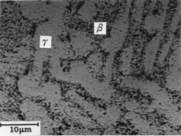
As shown in Fig. 1, the microstructure of the In-49Sn alloy before soldering reactions is composed of a lamellar Sn-rich ␥ phase and an In-rich  matrix. The In-49Sn eutectic solder possesses excellent wet-tability on Cu substrates (Fig. 2). The contact angles measured at temperatures above 200°C decline to
Phase Identification and Growth Kinetics of the Intermetallic
Compounds Formed During In-49Sn/Cu Soldering Reactions 641
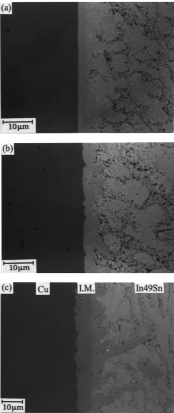
25° as the solder drops reach the melting point of 120°C. Below 200°C, the contact angles of the molten solder drops stay at 90° for several minutes and then collapse to attain the equilibrium value of 25°. The intermetallic compounds that appear at the In-49Sn/Cu interface after soldering reactions consist-ing of an elongated scalloped structure followed by a planar layer (Figs. 3 and 4). Chemical compositions of the intermetallic compounds formed at various temperatures are shown in Table I. The planar-inter-metallic layer possesses a composition (at.%) of Cu:In:Sn ⫽ 74.8:12.2:13.0, which corresponds to the ε-Cu3(In,Sn) phase. The composition of the elongated intermetallic scallops is Cu:In:Sn ⫽ 56.2:20.1:23.7, which corresponds to the -Cu6(In,Sn)5phase. It has been reported that the intermetallic compounds formed at the Sn/Cu,8,9Sn-Pb/Cu,10,11Sn-Ag/Cu,12,13 Sn-Bi/Cu,14–16and Sn-Cu/Cu17interfaces consist of a
Fig. 1. Microstructure of the eutectic In-49Sn solder.
Fig. 2. Contact angles (⌽) of In-49Sn solder drops on Cu substrates at various temperatures as a function of wetting time (t).
planar layer of Cu3Sn and a scalloped structure of Cu6Sn5. The intermetallic phases formed during the In-49Sn/Cu soldering reaction in this study are simi-lar to those in the preceding cases, except that the In element partially substitutes for Sn. From Table I, the Sn/In ⫹ Sn ratios in Cu3(In,Sn) and Cu6(In,Sn)5
intermetallic compounds are the same for the solder-ing reactions at the same temperatures. The Sn/In ⫹ Sn ratios in both intermetallic compounds decline slightly from 0.58 to 0.48 as the reaction tempera-ture rises from 150°C to 400°C. The Sn/In ⫹ Sn ra-tios in the reacted intermetallics are near the atomic percentage (0.48) of Sn in the In-49wt.%Sn solder. In addition, the compositions of the intermetallic com-pounds formed during the In-49Sn/Cu soldering
re-Fig. 3. Typical morphology of intermetallic compounds formed at In-49Sn/Cu interfaces after soldering reactions at various temperatures for 15 min: (a) 200°C, (b) 300°C, and (c) 400°C.
Fig. 4. Typical morphology of intermetallic compounds formed at In-49Sn/Cu interfaces after soldering reactions at various temperatures for 120 min: (a) 200°C, (b) 300°C, and (c) 400°C.
Phase Identification and Growth Kinetics of the Intermetallic
Compounds Formed During In-49Sn/Cu Soldering Reactions 643
actions (in liquid/solid state) are different from those reported in the literature for thermal-aging reac-tions (i.e., solid/solid state) at In-49Sn/Cu interfaces, where the intermetallic compounds were found to be Cu2In3Sn/Cu2(Sn,In) or Cu17Sn9In24/Cu26Sn13In8 dou-ble layers.1–7The difference in the compositions of the double layers, as reported by Roming et al.1 and Vianco et al.,2can be attributed to the disparate dip-ping conditions of both studies, which was already ex-plained by Vianco et al.2It has been shown that the predominant phases for the growths of Cu2In3Sn/ Cu2(Sn,In) and Cu17Sn9In24/Cu26Sn13In8 double lay-ers are Cu2In3Sn and Cu17Sn9In24, respectively. Obvi-ously, either Cu2In3Sn1,3–7or Cu17Sn9In24,2has grown close to the ␦ phase (CuIn2) formed during the In/Cu interfacial reactions.2In contrast, the Cu
3(In,Sn) and Cu6(In,Sn)5 intermetallics formed during the InSn(l)/Cu(s)reactions in our study are consistent with the εphase (Cu3Sn) and the phase (Cu6Sn5) present in the Sn/Cu interfacial reactions.8,9The results indi-cate that the low-melting-point In atoms become pre-dominant to react with Cu during the thermal-aging reactions of InSn(s)/Cu(s). However, the higher temper-ature range of InSn(l)/Cu(s) soldering reaction causes the higher-melting-point Sn to become the predomi-nate reaction agent.
From Figs. 3 and 4, it can also be seen that both types of intermetallic compounds grow with increas-ing reaction time and temperature. However, at tem-peratures below 300°C, the growth of scalloped inter-metallics (the phase) dominates over the planar-intermetallic layer (the εphase). In contrast, the planar-intermetallic layer grows much more rap-idly than the scallops at temperatures above 300°C. Consistent with the interpretation of Bader et al.9 for the formation of Cu3Sn intermetallic compounds at the Sn/Cu interface, the continuous Cu3(In,Sn) layer is also generated from the solid-state reaction between the scallop-shaped Cu6(In,Sn)5 inter-metallics and the Cu substrate: Cu6(In,Sn)5⫹ 9Cu → 5Cu3(In,Sn). The predominant growth of Cu3 (In,Sn) intermetallic compounds at temperatures above 300°C could be attributed to the acceleration of the aforementioned solid-state reaction at higher temperatures because of its higher activation ener-gies. Another explanation is that the maximum tem-peratures for (Cu6Sn5) and ε(Cu3Sn) phases in the Cu-Sn binary phase diagram are 415°C and 670°C,
respectively. The reaction temperatures above 300°C are near the maximum temperature of the phase, resulting in a lower chemical driving force for the formation of this type of intermetallic compound.
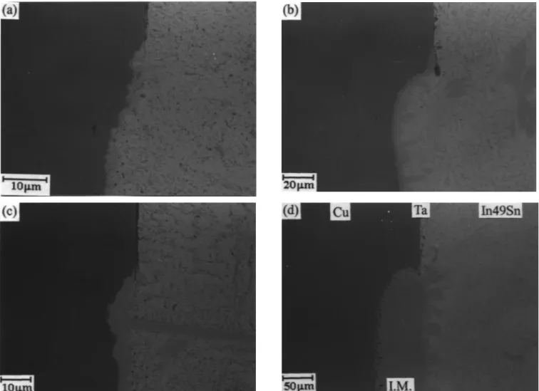
Through partial surface sputtering of the Ta-thin film on the Cu substrate as a diffusion barrier, the original In-49Sn/Cu interface can be distinguished. It can be observed from Fig. 5a and b that the Cu substrate is rapidly consumed at the early stage of soldering reactions, which results in the appearance of a concave interface. However, the thickness of in-termetallic compounds at the reacted interface is much less than the Cu thickness. The discrepancy is attributed to the severe spalling of intermetallic compounds away from the In-49Sn/Cu interface (Fig. 5c). With increased reaction time, the inter-metallic compounds fill in the region where Cu is consumed and grow toward the Cu substrate. It is interesting to note in Fig. 5c and d that the migrat-ing intermetallic compounds seem incapable of passing the original In-49Sn/Cu interfaces.
The growth kinetics for - and ε-intermetallic compounds is estimated by measuring the migra-tion distances of their respective reacmigra-tion fronts, i.e., the /solder and ε/ interfaces. In this way, the mi-gration distance of the ε-reaction front is equal to its phase width, while the distance for the -reaction front includes the width of the ε-intermetallic. It makes more sense using this method for kinetics analysis because the ε-intermetallic owes its growth to partial volume consumption of the -intermetal-lic: Cu6(In,Sn)5⫹ 9Cu →5Cu3(In,Sn).
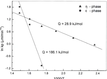
The measured migration distances (⌬X) of reac-tion fronts for - and ε-intermetallics versus the square root of reaction time are plotted in Figs. 6 and 7, respectively. The migration of both reaction fronts follows a parabolic-rate law, implying that the growths of both intermetallics are diffusion con-trolled. From the curves in Figs. 6 and 7, the reac-tion constants (kp ⫽ (⌬X/t1/2) can be calculated and plotted in Fig. 8 by applying the Arrhenius relation. The activation energies for the growths of - and ε -intermetallics, as obtained from the slopes of both Arrhenius plots, are 28.9 kJ/mol and 186.1 kJ/mol, respectively. The former value (28.9 kJ/mol) is con-sistent with the activation energy of Cu in liquid Sn (19.5 kJ/mol), as reported by Ma and Swalin.18The rate-limiting step for the growth of the
-inter-Table I. Chemical Compositions (at.%) of the Intermetallic Compounds Formed During In-49Sn/Cu Soldering Reactions at Various Temperatures
Temperature εPhase Phase
(ºC) Cu In Sn Cu In Sn 400 74.7 12.9 12.3 58.8 20.9 20.3 350 75.8 11.8 12.4 55.7 21.9 22.4 300 73.9 11.9 14.2 56.2 20.3 23.5 250 — — — 55.9 19.3 24.8 200 — — — 55.3 19.0 25.7 150 — — — 55.4 18.9 25.7
metallic toward the In-49Sn solder is the diffusion of Cu dissolved near the -reaction front into the sur-rounding liquid solder. The calculated activation en-ergy for the growth of the ε-intermetallic (186.1
kJ/mol) is close to the activation energies for the lat-tice diffusion of Sn and In in bulk Cu (187.6 kJ/mol and 178.0 kJ/mol, respectively).19,20 The growth of the ε-intermetallic is, therefore, believed to be
con-Fig. 5. Migration of intermetallic compounds during soldering reactions between In-49Sn solders and Cu substrates: (a) 250°C, 15 min; (b) 400°C, 15 min; (c) 250°C, 120 min; and (d) 400°C, 120 min. (The original In-49Sn/Cu interfaces are marked with Ta-thin films.)
Fig. 6. Migration distance (⌬X) of the -intermetallic compound formed at the In-49Sn/Cu interface as a function of the square root of time (t1/2).
Fig. 7. Migration distance (⌬X) of the ε-intermetallic compound formed at the In-49Sn/Cu interface as a function of the square root of time (t1/2).
Phase Identification and Growth Kinetics of the Intermetallic
Compounds Formed During In-49Sn/Cu Soldering Reactions 645
trolled by the lattice diffusion of Sn and In through the intermetallic compounds. The much higher acti-vation energy for the growth of the ε-intermetallic than for the -intermetallic can also explain why the growth of the ε-intermetallic becomes predomi-nant over the -intermetallic at higher tempera-tures.
CONCLUSIONS
Eutectic In-49Sn solder exhibits excellent wetta-bility on a Cu substrate. During the In-49Sn/Cu sol-dering reactions at temperatures ranging from 150–400°C, intermetallic compounds consisting of a planar layer and an elongated scalloped structure appear at the interface. The planar-intermetallic layer possesses a composition of Cu74.8In12.2Sn13, which corresponds to the ε-Cu3(In,Sn) phase. The scallop-shaped intermetallic compound is identified to be Cu56.2In20.1Sn23.7, which corresponds to the -Cu6(In,Sn)5 phase. In this study, the results ob-tained from the In-49Sn/Cu soldering reactions (liq-uid/solid) are different from those reported in other published work1–7on the thermal aging of In-Sn/Cu solder joints (solid/solid). The present experiments also show that the ε-intermetallic grows faster than the -intermetallic at temperatures above 300°C. By marking the original interface with a Ta-thin film, the Cu substrate is consumed rapidly to form a con-cave interface during the soldering reaction. As the
reaction time increases, the intermetallic com-pounds fill in the region where Cu is consumed and grow toward the Cu substrate. Kinetics analyses show that the growth of both - and ε-intermetallics are diffusion controlled. The calculated activation energy for the -intermetallic growth is 28.9 kJ/mol, which is relatively close to that for the diffusion of Cu in liquid Sn (19.5 kJ/mol). The result implies that the -intermetallic growth is controlled by the diffusion of dissolved Cu in the liquid solder. The ac-tivation energy for the ε-intermetallic growth is 186.1 kJ/mol, which is consistent with the activation energies for the lattice diffusion of Sn in Cu (187.6 kJ/mol) and In in Cu (178.0 kJ/mol). The ε -inter-metallic growth is thus concluded to be the diffusion of Sn and In in the intermetallic compounds.
REFERENCES
1. A.D. Roming, Jr., F.G. Yost, and P.F. Hlava, Proc. Conf. Mi-crobeam Analysis (San Francisco, CA: San Francisco Press, 1984), p. 87.
2. P.T. Vianco, P.F. Hlava, and A.C. Kilgo, J. Electron. Mater. 23, 583 (1994).
3. D.R. Frear and P.T. Vianco, Metall. Mater. Trans. A 25A, 1509 (1994).
4. J.L. Freer Goldstein and J.W. Morris, Jr., Metall. Mater. Trans. A 25A, 2715 (1994).
5. J.L. Freer Goldstein and J.W. Morris, Jr., J. Electron. Mater. 21, 647 (1992).
6. J.L. Freer Goldstein and J.W. Morris, Jr., J. Electron. Mater. 23, 477 (1994).
7. J.W. Morris, Jr., J.L. Freer Goldstein, and Z. Mei, JOM 45, 25 (1993).
8. K.N. Tu and R.D. Thompson, Acta Metall. 30, 947 (1982). 9. S. Bader, W. Gust, and H. Hieber, Acta Metall. 43, 329
(1995).
10. H.K. Kim, H.K. Liou, and K.N. Tu, Appl. Phys. Lett. 66, 2337 (1995).
11. C.Y. Liu, K.N. Tu, T.T. Sheng, C.H. Tung, D.R. Frear, and P. Elenius, J. Appl. Phys. 87, 750 (2000).
12. W. Yang and R.W. Messler, J. Electron. Mater. 23, 765 (1994).
13. C.H. Raeder, L.E. Felton, V.A. Tanzi, and D.B. Knorr, J. Electron. Mater. 23, 611 (1994).
14. H.K. Kim, H.K. Liou, and K.N. Tu, J. Mater. Res. 10, 497 (1985).
15. P.T. Vianco, A.C. Kilgo, and R. Grant, J. Electron. Mater. 24, 1493 (1995).
16. C. Chen, C.E. Ho, A.H. Lin, G.L. Luo, and C.R. Kao, J. Elec-tron. Mater. 25, 1113 (1996).
17. Y.G. Lee and J.G. Duh, Mat. Charact. 42, 143 (1999). 18. C.A. Ma and R.A. Swalin, Acta Metall. 8, 388 (1960). 19. R.L. Fogelson, Y.A. Ugay, and I.A. Akimova, Fiz. Met.
Met-alloved. 37, 1107 (1974).
20. W. Gust, C. Ostertag, B. Predel, U. Roll, A. Lodding, and H. Odelius, Philos. Mag. A47, 395 (1983).
Fig. 8. Arrhenius plots of growth rate constants (kp) for the inter-metallic compounds formed during In-49Sn/Cu soldering reactions.