Circuit Modeling and Noise Reduction for Bent Differentid Transmission Lines Guang-Hwa Shiue, Wei-De Guo, Li-Shang Liu, and Ruey-Beei
Wu
Department of Electrical Engineering and Graduate Institute of Communication Engineering National Taiwan University, Taipei, 10617, ROC..
Email: rbwu@bv.ntu.edu.tw Abstract
Differential signaling has become a popular choice for multi-gigabit digital applications, due to its low noise generation and high common-mode noise immunity. This paper describes a methodology to extract the equivalent circuits of the discontinuities for strongly coupled differential lines fiom the calculated full-wave S-parameters. The signal integriw effects of the bent differential transmission lines in a high-speed digital circuit is then simulated in time domain. A new way to reduce the common mode noise at
the
receiver by shunt compensation capacitances is also proposed.1. Modelsetup
Differential signaling is fbquently employed in PC board designs for high-speed digital systems. It is quite common that the signal traces
ak
bent for practical layout consideration To investigate the signal integrity issues of these bends, it is necessary to develop lumped and frequency-dependentequivalent circuits for the discontinuities [l]
For example, consider a bent differential line shown in Fig.l(a). Sinee the size
of
the bends is usually much smallerthan
the wavelength of the considered frequency range,the
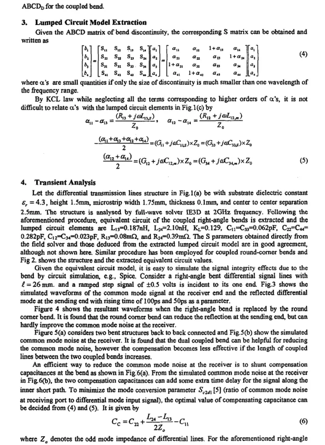
structure can be modelled as Figl@) where the bend can be approximated by a simple lumped circuit shown in Figl(c).This
lumped circuit model is an extension of the R model used for bend of a single bansmission line. Though this model can include radiation, conductor and dielectric losses as jhquency dependent resistance, these losses are smalI and negligible for practical applications up to Gbps rates.2. De-embedding Technique for Strongly Coupled Structures
Most ofthe present commercial EM field solvers assume isolated output ports in de-embedding the transmission l i e effects. When the input/output trwsmission lines are strongly coupled, a more general approach need be developed. For simplicity, consider a system of N bent coupled transmission lines. By using field solvers, its lidl wave characteristics can be modeled in terms of a 2N-port ABCD mamix. Based on the cascade property, the ABCD matrix can be divided into three parts: two sections of coupled transmission lines and a bend structure in between
As
show in Fig.@), the ABCD matrix can be formulated as[;I=[
-C,':
-!t].k
D, CD DD ! D ] . pe,
B,
"].[;]=p
CO ;].[Do !o](1) where the SubscriDt "D" denotes for the bend and
"P"
for a section of the coupled " m i s s i o n lines WithlengthP.To de-embed the transmission lines, consider a section of coupled msmissiou lines of length
2 P .
Its ABCD matrixcan
be formulated as(2) It is readily available that the ABCD matrix of a single transmission line assuming quasi-TEM mode propagation satisfies the property
(3) The ABCDt matrix can be solved fiom (2) and then substituted into (1) to extract the desired
n e workwas supplied in part by IheNational Science Council. Republic ofChina, under GrantNSC 91-2213-E-002-109.
ABCD, for the coupled bend
3.
Lumped
Circuit ModelExtraction
written asGiven the ABCD matrix of bend discontinuity, the corresponding
S
matrix can be obtained and(4)
I + % a,, a,,
where a's are small quantities if only the size of discontinuity is much smaller than one wavelength of the frequency range.
By KCL law while neglecting all the terms corresponding to higher orders of a's, it is not difficult to relate a ' s with the lumped circuit elements in Fig.l(c) by
( 4 3 + j 4 d
,
a,, -a,, =(4,
+ j & , )2, ZO
4, -al, =
4. Transient Analysis
Let
the differential transmission lines structure in Fig.l(a) be with subshate dielectric constantE, = 4.3, height 1.5mm, microstrip width 1.75". thickness O.lmm, and center to center separation 2.5mm. The structure is analysed by full-wave solver IE3D at 2GHz frequency. Following the aforementioned procedure, equivalent circuit of the coupled right-angle bends is extracted and the lumped circuit elements are L1~0.187nH, L~4=2.lOnH, KL=0.129, ClI=Cu=0.062pF. C,=C,= 0.282pF, G ~ C 3 ~ 0 . 0 2 3 p F , 43=0.08mQ, and R%=0.39&. The S parameters obtained directly from the field solver and those deduced from the extracted lumped circuit model are in good agreement, although not shown here. Similar procedure has been employed for coupled round-comer bends and Fig 2. shows the structure and the extracted equivalent circuit values.
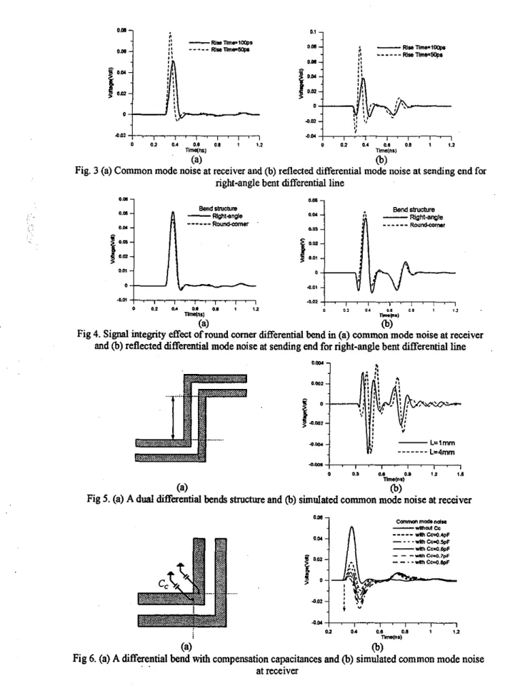
Given the equivalent circuit model, it is easy to simulate the signal integrity effects due to the bend by circuit simulation, e.g., Spice. Consider a right-angle bent differential signal lines with
e
= 26 mm. and a ramped step signal of kO.5 volts is incident to its one end. Fig.3 shows the simulated waveforms of the common mode signal at the receiver end and the reflected differential mode at the sending end with rising time of loops and 50ps as a parameter.Figure 4 shows
the
resultant wavefonns when the right-angle bend is replaced by the round comer bend. It is found that the round comer bend can reduce the reflection at the sending end, but can hardly improve the common mode noise at the receiver.Figure 5(a) considers two bent shuchues back to back connected and Figs@) show the simulated common mode noise at the receiver. It is found that the dual coupled bend can be helpful for reducing the common mode noise, however the compensation becomes less effective if the length of coupled limes between the two coupled bends increases.
An efficient way to reduce the common mode noise at the receiver is to shunt compensation capacitances at
the
bend as shown in Fig.6(a). From the simulated common mode noise at the receiver in Fig@), the two compensation capacitances can add some extra time delay for the signal along the innershort
path To minimize the mode conversion parameterS
,
,
,
[SI
(ratio of common mode noise at receiving port to differential mode input signal), the optimal value of compensating capacitance can be decided from (4) and (5). It is given by(6)
c,
=c,+
L a -43 d-,22,
where Z, denotes the odd mode impedance of differential lines. For the aforementioned right-angle
bend structure, the optimal compensating capacitance can be calculated to be about 0.6pF. The simulated results in Fig6 validate the correctness of (6). Also, the maximum common-mode noise versus the compensation capacitance is listed
in
Table 1. For the present example. the employment of compensation capacitances reduces the common mode noise by 53%.5. Conclusions
Based on the cascade property of the
ABCD
matrix, a systematic procedure has been established to e m c t lumped circuit model for discontinuities of differential lines. The circuit model can be employed to investigate the signal integrity issues of the discontinuities on high-speed digital signals. The round caner bend can reduce the reflection at the sending end, but can hardly improve the common mode noise at the receiver. Two bent smctures back to back connected closely is one way toreduce the common mode noise. Insertion of compensation capacitances is another effective way. References
[l] R 2. Mu and K Will& "SI and eonsiderations for Gbps PCBs in Communication systems," EIecfricaI Petfbmance ofEfechtmic Packaging C o ~ . Oct 200 I .
121 P. H. Harms and R. h4im "Equivalent circuits for multioonductor microstrip b f d discontinuities," IEEE Tram. Microwwe TheqTech.. Vo1.41, Jan 1993.
[3] D. M Po=, Miuowow Engineering. Second Edition, New York: Wiley, 1998.
[4j J. Lee, S. Ahn, J. Ryu, and J. Kim, "Over 20 GHz microwave ti-equency model of fme pitch ball grjd m y
[SI W. Fan, A Ly L. L. Wai, and E. K. hk, "Mixed-mode S-parameter characterization of differential
(FPBGA) bonding," Ekcfricol P e t f m n c e ofElecfronic Packaging Conj, 2000.
structures." 5ih EIectronicsPackoging Technology CO& pp. 533-537, Dec. 2003.
Fig 1.Bent coupled transmission line. (a) layo$ (b) block diag". and (c) equivalent circuits
Table 1. Maximum common mode noise versus compensation capacitance
Fig 2.EquivaJent circuit of round comer bends
Fig. 3 >
io-{
om I 0 0 1 I. 0.1 0 8 t t.2 0 0 1 0 4 I D OB I 1.1 Tlmqml tmeln.1 (a) (b)(a) Common mode noise at receiver and (b) reflected differential mode noise at sending right-angle bent differential line
end for *.m
::L
---
---
R O “ n b ” ,!I
0.m 0 4.0, .om .*.e 0 0.2 0” 01 0.4 (2 I 0 1 0. * I 0 1 I!,
w n r i Tk.l”.l (a)(3)
Fig 4. Signal integrity effect of round comer differential bend in (a) common mode noise at receiver and (b) reflected differential mode noise a! sending end for right-angle bent differential l i e
(a)
Fig 5. (a) A dual differential bends structure and (b) simulated common mode noise at receiver
(a) (a)
Fig 6. (a) A differential bend with compensation capacitances and , . @) simulated common mode noise
at receiver