TRIANGULAR-ELEMENT
FINITE-ELEMENT ANALYSIS OF A
TRAPEZOID POLYMER OPTICAL
WAVEGUIDE
Shyh-Lin Tsao,1Jingshown Wu,2and Yue-Loong Her2 1Department of Electronic Engineering
St. John’s and St. Mary’s Institute of Technology Tamsui, Taiwan
2Department of Electrical Engineering
National Taiwan University Taipei, Taiwan, Republic of China
Recei¨ed 3 December 1996
ABSTRACT: Because of mechanical properity, polymer optical wa¨ e-guide interconnections can increase design flexibility. In this article we analyze the propagation characteristics of the trapezoid polymer optical wa¨eguide by use of the finite-element method with triangular elements. The trapezoid polymer optical wa¨eguide promises a larger cutoff fre-quency o¨er the con¨entional rectangular wa¨eguide.Q 1997 John Wiley & Sons, Inc. Microwave Opt Technol Lett 15: 87]89, 1997.
Key words: polymer optical wa¨eguide; finite-element method
I. INTRODUCTION
The switching time of electronic devices and the chip integra-tion scale have been improved greatly recently, and hard-wire transmission delays have become the crucial bottleneck on the system. Because the optical interconnection can meet the requirements of high density, high speed, and low cost for VLSI fabrication and replacement of electrical transmission line, it becomes increasingly important for high-speed
com-w x
puters or communication systems 1, 2 . At higher data rates Žabove 1 Gbps , as the lengths of interconnections within chip.
Ž .
and from chip to chip increase above 1 mm , the optical w x
interconnections have lower power dissipation 3 .
In this Letter, we study the trapezoid and rectangular polymer optical waveguides for optical interconnections. The dispersion relation is analyzed by use of the finite-element method with triangular elements, which can provide the ben-efit of defining the tilt angle of the roof slope. In this work we find that the trapezoid waveguide can provide higher cutoff frequency than the rectangular waveguide with the same refractive indices and geometrical scale.
II. TEFEM ANALYSIS
Many microwave or optical waveguides have been analyzed
Ž .
with the use of the finite-element method FEM . The
trian-Ž .
gular element finite-element method TEFEM has become especially popular for investigating nonrectangular
wave-w x
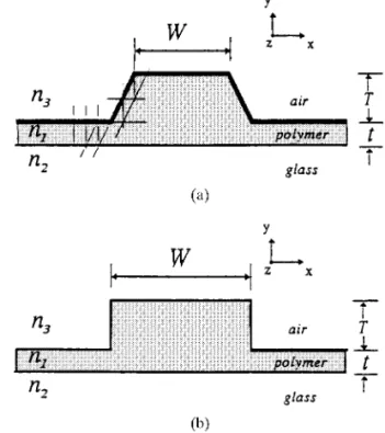
guides 4, 5 . A trapezoid optical waveguide and a rectangu-lar-type waveguide, along with their geometrical parameters,
Ž . Ž .
are shown in Figures 1 a and 1 b , respectively. The electro-magnetic field propagating along the z-axis in the waveguide
w Ž .x
can be expressed as expyj b z y vt , where z is the propa-gation direction, b is the propagation constant in the z direction,v is the angular frequency, and t is time. To apply the TEFEM, we discretize the cross section of the optical waveguide by suitable triangular-edged elements, as shown in Figure 2. The triangular element consists of three corners, whereas the local corners numbered 1]3 proceed counter-clockwise for the z-axis field f . The other three sides,z
Ž labeled 4]6, represent the tangential component f : in-t
Ž . Ž .
Figure 1 a Cross section of trapezoid waveguide, b Cross section of rectangular-type waveguide
Figure 2 Schematic diagram of triangular elements
.
cludes both x-axis and y-axis field components . Assuming the optical waveguide to be isotropic and using Maxwell’s equations, we can represent the vectorial Helmholtz equation as 2 2 Ž . = = = = F y k n F s 0,0 1 Ž . F sf e q f e q f e ,x x y y z z 2 Ž
where F denotes either E or H, k0 s 2prl, l is the
.
wavelength is the free-space wave number, and n is the refractive index of the polymer waveguide. With the use of the variation method to solve the partial differential
w x Ž . tions 6 , we derived the functional for Eq. 1 as
wŽ . Ž . 2 2 x Ž .
Fs
HH
= = F * ? = = F y k n F* ? F dx dy. 30 VHere the asterisk denotes the complex conjugate and V is the waveguide cross-section area where the integration is performed over it. The optical transverse componentsf , f ,x y and axial componentf of the electromagnetic field vector Fz can be approximately represented as three first-order
polyno-w x
mials 5 in x and y, respectively, such that T w x w x Ž . f s Sx x f ,t e 4 T w x w x Ž . f s Sy y f ,t e 5 T w x w x Ž . f s Sz z f ,z e 6 w x w x w x
where S , S , Sx y z are the shape function vectors for the triangular edge elements, the superscript T denotes the
in-w x w x
verse matrix, and fz e and ft e are the z-axis field vector and the edge tangential-field vector for each element, respec-tively. The coordinate relation between the transverse com-ponents f , f and tangential component f can be gener-x y t ally expressed as
Ž .
f s f cos u q f sin u ,t x y 7
whereu is the tilt angle between the x axis and the edge of
Ž . Ž .
f . If we substitute Eq. 3 into Eq. 2 , apply the variationalt principle, and then solve the eigenvalue equations to get the propagation constant b, we can calculate the normalized refractive index b from the following equation:
2 2
Žbrk0. y n2
Ž .
bs 2 2 , 8
n1y n2
where n and n1 2 are the refractive indices of the polymer waveguide and silica, respectively. The normalized frequency n is defined as
Ž . Ž .
n s T q t rl, 9
where Tq t is the thickness of the trapezoid polymer wave-guide.
III. EXPERIMENTAL AND NUMERICAL RESULTS
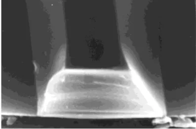
We fabricate a trapezoid polymer optical waveguide on silica substrate by using an embossing method with the Si mold, which is prepared by micromachining. The cross section of the fabricated trapezoid polymer optical waveguide using
Ž . Ž .
PMMA n1s 1.491 on silica substrate n s 1.453 is shown2
in Figure 3. Because of anisotropic etching on the Si wafer, the tilt angle is 54.78. We apply TEFEM to analyze the
Ž propagation characteristics of the trapezoid waveguide u s
. Ž .
54.78 and the rectangular waveguide u s 908 . The numeri-cal result is shown in Figure 4, the cutoff frequency of the trapezoid waveguide is located at n s 1.5, which is larger than the cutoff frequency of the rectangular waveguiden s
Ž .
1.3. By selecting small Dn Dn s n y n1 2 and large Dt ŽDt s T y t , we can increase the cutoff frequency of the. waveguide. Also, we find that the trapezoid optical waveguide promises a larger cutoff frequency over the conventional rectangular waveguide.
Figure 3 SEM micrograph of the cross section of trapezoid poly-mer optical waveguide
Figure 4 Comparison of propagation characteristics between opti-cal trapezoid waveguide and rectangular waveguides. Solid lines, trapezoid waveguide; dashed lines, rectangular waveguide
IV. CONCLUSIONS
Due to large bandwidth and minimal cross talk, the polymer optical interconnection will play an important role in optical interconnections in the future. The cheap organic polymer optical waveguide has presented great potential. In this arti-cle we use the TEFEM method to analyze the propagation characteristics of a trapezoid polymer optical waveguide.
The results show that the single-mode trapezoid polymer waveguide can have wider width and larger thickness than the rectangular waveguide. We believe that the trapezoid poly-mer waveguide may become an attractive choice as more advancements are made in developing polymers with better characteristics.
ACKNOWLEDGMENT
The authors would like to thank Dr. Ruey-Beei Wu and Dr. Way-Seen Wang for useful discussions and assistance. This work was supported in part by the National Science Council under Contract Nos. 2215-E-129-002 and NSC86-2215-E-002-028.
REFERENCES
1. L. D. Hutcheson and P. Hangen, ‘‘Optical Interconnects Replace Hardwire,’’ IEEE Spectrum, Vol. 1, 1987, pp. 30]35.
MICROWAVE AND OPTICAL TECHNOLOGY LETTERS / Vol. 15, No. 2, June 5 1997
2. R. Selvaraj, H. T. Lin, and J. F. Mcdonald, ‘‘Integrated Optical Waveguide in Polymide for Wafer Scale Integration,’’ IEEE J.
Lightwa¨e Technol., Vol. LT-6, 1988, pp. 1034]1044.
3. R. A. Nordin, F. J. Levi, R. N. Nottenburg, J. O’gorman, T. Tanbunek, and A. R. Logan, ‘‘A System Perspective on Digital Interconnection Technology,’’ IEEE J. Lightwa¨e Technol., Vol.
LT-10, 1992, pp. 811]827.
4. B. M. A. Rahman and J. B. Pavies, ‘‘Finite-Element Analysis of Optical and Microwave Waveguide Problem,’’ IEEE Trans.
Mi-crowa¨e Theory Tech., Vol. MTT-32, 1984, pp. 20]28.
5. M. Koshiba and K. Inoue, ‘‘Simple and Efficient Finite Element Analysis of Microwave and Optical Waveguides,’’ IEEE Trans.
Microwa¨e Theory Tech., Vol. MTT-40, 1992, pp. 371]377. 6. M. N. O. Sadiku, Numerical Techniques in Electromagnetics, CRC
Press, Boca Raton, FL, 1992, pp. 259]266.
Q 1997 John Wiley & Sons, Inc. CCC 0895-2477r97
A GAIN-ENHANCED PROBE-FED
MICROSTRIP PATCH ANTENNA OF
VERY HIGH PERMITTIVITY
Y. P. Zhang,1Y. Hwang,1and G. X. Zheng2 1
Department of Electronic Engineering City University of Hong Kong
Kowloon, Hong Kong
2Institute of Confined Space Communications
Taiyuan University of Science and Technology Shanxi, People’s Republic of China
Recei¨ed 3 December 1996; re¨ised 17 January 1997
ABSTRACT: A probe-fed microstrip patch antenna in a¨ery high permitti¨ity substrate]superstrate configuration has been experimentally
in¨estigated at 1.8 GHz. The microstrip patch is much smaller and has about the same gain as a con¨entional microstrip patch.Q 1997 John
Wiley & Sons, Inc. Microwave Opt Technol Lett 15: 89]91, 1997.
Key words: microstrip antenna; high-permitti¨ity materials
I. INTRODUCTION
In recent years low-loss temperature-stable
high-relative-per-Ž .
mittivity « s 37, 80 materials have received attention be-r cause they play a role in miniaturizing rectangular microstrip
w x
patch antennas for personal communication systems 1, 2 . It has been shown that a direct application of a high-relative-permittivity material to reduce the dimensions of a rectangu-lar microstrip patch antenna is accompanied by a substantial w x reduction in antenna bandwidth and gain. As indicated in 3 , with a substrate of permittivity of 100, the dimensions of the patch were reduced by a factor of 10, but the radiation efficiency was reduced to 12% for a bandwidth of 0.5%. Therefore the enhancement of the bandwidth and gain of microstrip patch antennas of high permittivity is highly desir-able. Perrotta and Hoofar have improved the bandwidth by cutting two parallel slots in their rectangular microstrip patch on a high-permittivity substrate and optimizing the locations
w x
of the slots 2 . Here we have enhanced the gain of a
Ž .
microstrip patch on a high-permittivity « s 38 substrate byr
Ž .
adding two layers of high permittivity « s 38, 80 super-r
w x
strates 4]6 . It is shown that a more than 10-dB gain can be achieved.
II. ANTENNA CONFIGURATION
The configuration of the microstrip patch antenna is shown in Figure 1. The rectangular microstrip patch is on a very high
Ž .
permittivity « s 38 substrate, and is covered by two layersr
Ž .
of superstrates of different high-permittivity « s 38, 80 ma-r terials. The dimensions of the rectangular microstrip patch are A and B. The thickness of the substrate and superstrates one and two are t , t , and t , respectively. The rectangular1 2 3
Ž .
microstrip patch antenna is excited by a probe at x , y .p p Three rectangular microstrip patch antennas designed at 1.8 GHz are listed in Table 1. The first two single-layer antennas are used as references. The third antenna is the gain-enhanced one, which has two layers of superstrates of
Ž .
different high-permittivity « s 38, 80 materials. The thick-r
Ž .
ness of two superstrates is 1.34 mm 0.04960l and 3.35 mm2
Ž0.1799l , respectively. Compared with the size of the first3. reference antenna, the sizes of the patches of the second reference antenna and the gain-enhanced antenna are ap-proximately reduced by 9.7 and 11.45 times, respectively.
III. EXPERIMENTAL RESULTS
Figure 2 shows the measured return loss as a function of frequency. The dash-dot curve depicts the measured return loss of the gain-enhanced antenna. The solid and dashed curves display the measured return losses of reference an-tenna one and two, respectively. It is seen that good matching has been achieved for all three antennas. The antennas are
< <
resonant at 1.8 GHz. Using S11F y10 as a criterion, the
Ž .
measured impedance bandwidths are 19.5 MHz 1.083% for
Ž .
the first reference antenna, 19.5 MHz 1.083% for the
sec-Ž .
ond reference antenna, and 16.5 MHz 0.917% for the gain-enhanced antenna.
Ž . Ž .
Figures 3 a and 3 b show the copolarized E- and H-plane radiation patterns of three antennas, respectively. The upper
Ž .
and lower continuous curves in Figure 3 a represent the relative received power by reference antennas one and two. The corresponding maximum relative received powers are y32.2 dBm and y43.7 dBm. The impact of adding two superstrates with optimal thickness can be seen from the
Figure 1 Geometry of the gain-enhanced rectangular microstrip patch antenna