Novel dead1 time
compensation method for
induction motor drives using space vector
m od u
I
at
i o
n
Y.-H.LiuC.-L.Chen
Indexing terms: Induction motor ,drives, Dead-time compensation
Abstract: A novel dead time compensation
method is proposed. The method calculates the difference between the ideal output voltage and the real one, and then compensates the effect via modification in the original controller software. This method can be applied to all controllers utilising space vector modulation techniques. The proposed approach will not affect the operating speed of the controller, and no additional hardware is needed. Simulation and experimental results illustrate the effectiveness of the proposed method.
Introduction
Current-controlled voltage-fed pulsewidth modulation (PWM) inverters are widely employed in motor drive systems. In some applications, such as sensorless vector control and direct torque control systems, the inverter output voltages are needed to calculate desired state variables [ 1-51. However, the inverter output voltage consists of a low fundamental frequency and modu- lated discrete pulses at switching frequency. There are two major ways that are often used to measure the inverter output voltage. The first is by using a lowpass filter to measure the oui:put voltage, but this method is not practical in most applications because the lowpass filter will result in time delay in the control system. The second way to obtain the output voltage is to use the reference voltage as the output voltage. This method is rather simple to implement, but in practice there are some differences between the reference voltage and the real output voltage. The difference between the two voltages is mainly caused by the dead time that is essential to prevent the ;jhoot-through phenomenon. To solve this problem, remarkable efforts have been pro- posed to compensate the effects of dead time [6-91. In [6], compensation time is calculated from q-axis stator voltages and currents, and then the switching signal is adjusted to compensate for the dead time effect. In [7],
0 IEE, 1998
IEE Proceedings online no. 199 3 1867
Paper first received 11th September 1997 and in revised form 5th January 1998
The authors are with the Power Electronics Laboratory, Department of Electrical Engineering, National Taiwan University, Taipei, Taiwan
compensation signals are obtained frlom the Zq - 1, cur-
rents and inverter output angular frcquencies, then the compensation is accomplished by applying the modi- fied switching signals. In [8], compensation for the dead time effect is accomplished by adjusting the pulse times of the waveform generator prior to the dead time coun- ter. All these methods described above adjust the switching signals produced by the controller to com- pensate for the dead time effect. Although these meth- ods all demonstrate very good Compensation results, they require precise control on the switching time instant to acquire better performance. Also, to obtain the desired compensation switching signals, compli- cated computations are needed in these methods. In [9], the dead time effect is compensated for by a current prediction feature, and this method requires extra hard- ware to implement.
In this paper, a novel dead time compensation method is proposed. This method compensates for the dead time effect by modifying the controller software. The proposed method is applicable for all the motor control methods that utilise the space vector modula- tion technique. It is simple and no additional hardware is required: only slight modification in the software is needed. The proposed method will increase the control- ler performance without degrading it s speed.
Simulation and experiments are reported in this paper. Both show the effectiveness of the proposed method.
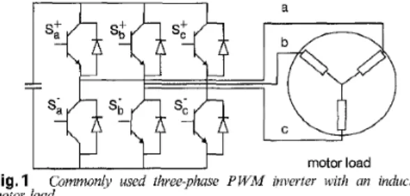
motor load
Fig. 1
moioy load Commonlv used three-phase P W M inverter with an induction
2 Description of proposed method
Fig. 1 shows a commonly used three-phase PWM inverter with an induction motor load. In Fig. 1, three inverter legs are connected to the a. b and c phases of
the motor, respectively. S,C, S i and S,+ represent the switching signals that are applied to the upper switches, and S i , S b and
Sp
represent the corresponding switching signals of the lower switches.387
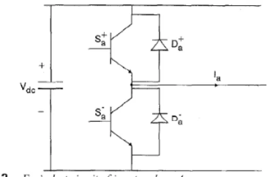
Ideally, switching signals of a gating signal pair for the same phase are complemented. That is, S i turns on at the exact instant when S i turns off, and vice versa. However, in practice, most switching devices have their turn-off delay time due to the carrier storage effect. So if S i turns on immediately after S i turns off, then two switches on the same inverter leg will conduct simulta- neously. To avoid short-circuits of the bridge legs, a delay time Td must be introduced into the inverter con- trol. The delay time is often called the dead time and is set as the maximum value of storage time plus a safety margin.
t---
'h-
a
b
Fig.2
a Ideal case, b practical output voltage vector case of inverter
Because of dead time effects, the output voltage of an inverter will differ from the reference voltage. Thus, a compensation technique is required. This concept can be illustrated by Fig. 2. Fig. 2a shows the ideal case of an inverter switching interval, where t h represents the switching time interval and V , represents the reference voltage vector applied to the motor load. Convention- ally, V , is determined by a voltage estimator which cal- culates V , as a function of switch states, and the equivalent output voltage vector of an inverter during one switching interval can be calculated as V,th. Fig. 2b shows the practical case of an inverter switch- ing interval, where td represents the dead time interval and Vd represents the voltage vector applied to the motor load during dead time. In Fig. 2b, the output voltage of the inverter can be calculated as Vdtd
+
V,(th- td). From Fig. 2, the difference between the ideal case
and the practical one is (V, - Vd)t,.
should not change rapidly. Accordingly, two different cases may exist and the associated voltage vector V d
can be determined.
Case L I, > 0, the current flows through the switch S,t or diode D ; . During the dead time intervals,
5':
andS i are both turned off, but the current I, should be continuous because of the inductive motor load. Thus the current should flow through
D ;
in this time inter- val, which implies that phase a is connected to the neg- ative terminal of the DC bus.Case II: I, < 0, the current flows through the switch S ; or diode 0,'. During the dead time intervals, Si and S i are both turned off but the current I, should be continuous because of the inductive motor load. Thus the current should flow through 0,' in this time inter- val, which implies that phase a is connected to the pos- itive terminal of the DC bus.
T '
Fig. 4 All possible voltage vectors of an inverter
The terminal voltages of phases b and c can be deter- mined in the same way. Therefore, by considering the polarities of i,, ib and i, during the dead time interval,
we can determine which terminal of the DC bus the three phases a, b and c are connected to. Then we can obtain the resulting voltage vector Vd accordingly. Table 1 illustrates the resulting voltage vector V d under different current polarities. All the vectors are defined in Fig. 4.
Table 1: Voltage vector V, under different current polari- ties
Sign of i, Sign of ih Sign of i, Resulting voltage vector V, 'a
Fig.3 Equivalent circuit of inverter phase A
Thus, it is desirable to determine the voltage vector during the dead time. Let us take phase a of the inverter, for example. Fig. 3 shows the equivalent cir- cuit of the inverter phase a, where I, represents the cur- rent that flows to phase a of the induction motor load. Because the motor is an inductive load, the current I,
388
Using some mathematical manipulations, Table 1 can be summarised into a simple equation. If we define
t z
= ( - l ) s g n ( Z a s )t ,
= [sg.(ics) - sgn(&)]/2Then Table 1 can be simplified as follows. The voltage vector Vd can be calculated as Vd = VA, where
(1)
3
2
n
-(1 -t z )
+
t,t,
+
1
if A =0
then A = 6.The proposed method (can now be applied to applica- tions that use the inverter output voltage to calculate the desired state variables. The only modification is to replace the original voltage vector Vxth with Vx(th - t d )
+
V d t , where Vd can be calculated using eqn. 1. Simulation and experiinental results are presented in the following Section to (demonstrate the validity of the proposed method.3 Simulation and experimental results
In this Section we applj the proposed method to two motor control applications which use the inverter out- put voltage to calculate the desired state variables. These two applications are the sensorless vector control system and direct torque control system. Simulations and experiments are carried out to illustrate the dead time effects on these two methods, and comparison will also be made to demonstrate the effectiveness of the proposed method. All simulations and experiments are performed on a 3 hp induction motor. The motor parameters are listed in the Appendix.
ia
inverter
transformation
Fig.5
together with proposed compensarion method Simplified
block diagrm of U sensorless vector control system
3,
I
Sensorless vec:tor control applications
In this Section we apply the proposed method to a sen- sorless vector control sy!;tem and analyse the dead time effects under compensaied and uncompensated condi- tions. Fig. 5 shows a simplified block diagram of a sen- sorless vector control system together with the proposed compensation method. The speed observer used in Fig. 5 is an adaptive observer proposed by Kubota et al. [2]; the modulation method used here is space vector modulation. In Fig. 5 , the inverter switch- ing signals are used to estimate the output voltage vec- tor, then the speed observer utilises the output voltage vector together with motor input currents to estimate the desired motor speed. It is evident that the calcu- lated output voltage will be incorrect if the dead time effect is not considered, and thus a more accurate out- put voltage vector can 13e obtained when applying the proposed method (cross-hatched area) to the sensorless vector control system.
In the sensorless veci.or control system, the output voltage vector is required to calculate the estimated motor rotating speed, which directly affects the speed
control characteristics of' the controller. In this kind of application, different factors will result in different amounts of dead time effects. They are the speed com- mand value, load torque value, dead time duration and IEE Proc.-Electr. Power Appl., Vol. 145, No. 4 , July 1998
switching frequency. Fig. 6 shows the speed percentage error Aol,/w* under different speed command values. The dead time duration is fixed as 3 1 s and the switch- ing frequency is set
as
10kHz. From ]Fig. 6 it can easily be observed that the speed percentage error decreases as the speed command increases. The reason is that voltage distortion will not dependon
the fundamental voltage, hence its influence is very strong in the low speed range where the fundamental voltage is low.EO
t p 2
20 50 80 100 120 150 180 200 speed command, rad/s
Fig. 6 Speed percentage error under dflerent sFleed command vulues
load conditions, Nm
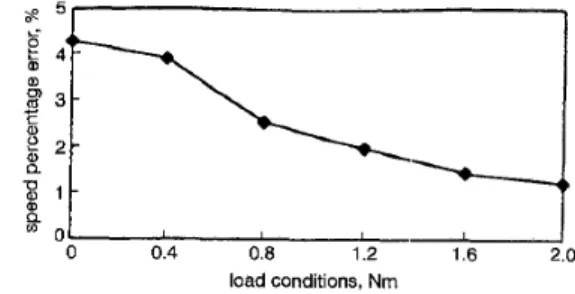
Speed percentage error under dij@rent loading conditions Fig. 7
Fig. 7 shows the speed percentage error Bolo* under different loading conditions. From Fig. 7, the dead time effect becomes apparent as the load decreases. The reason is that the dead time effect can be regarded as an equivalent voltage drop. So under light loading con- ditions, this voltage drop results in a more serious problem.
Fi .8
wiiout dead Speed error against dead time durations und switching time compensation frequency,
Figs. 8 and 9 show the speed error Am against dead time duration and switching frequency without and with dead time effect compensation, respectively. The
speed command is set as 200 rad/s and the load torque value as 0. Observing Figs. 8 and 9, different dead time durations produce different speed errors. In lower switching frequencies, the speed error is large because a low switching frequency implies slower control, but the
difference between maximum and minimum speed errors is smaller than for high switching frequency cases. It is because, in lower switching frequencies, dead time occupies a smaller proportion of total switching time intervals. For example, if dead time = 3ps, then it will occupy 0.6% of the switching time interval when the switching frequency = 2kHz. The same dead time will then occupy 3% of the switching time interval when the switching frequency = 10kHz. Conversely, a higher switching frequency implies faster and better control, but the dead time effects will become more apparent as the dead time durations increase. Comparing Figs. 8 and 9, it can be observed that the speed error of Fig. 9 is always smaller than that of Fig. 8, especially in higher switching frequency regions. This can be further illustrated by Fig. 10, which shows the total speed error of different switching frequencies under different dead time durations. From Fig. 10, the total speed error of the compensated controller under each dead time duration is always smaller than that of the uncompensated controller.
-
10Speed error against dead time durations and switching frequency,
Switching frequency, kHz
Fi .9
w i x dead time compensation
From Fig. 11, the actual voltage is equal to the esti- mated voltage and is different from the desired voltage. The effectiveness of the proposed method is guaran- teed. Fig. 12 shows the experimental result of the pro- posed method. Fig. 12a shows the speed response of both the uncompensatedkompensated controller, and Fig. 126 shows the zoomed version of the speed response for t = 4.0-5.0s. In this experiment, the speed command is 188.5 radis and switching frequency is 5kHz. From Fig. 126, the average speed error of the uncompensated controller is 4.3 radis, and the average speed error of the compensated controller is 0.9 radis.
1000 800 ._ 600 $ 400
.
ei 200 -200 0 1 O : time. s 3 4 5 c 910 E a, 900 i 890 ._.
uncompensated 880 4.0 4.2 4.4 4.6 4.8 5.0 time, s b Experimental step response resultsFig. 12 a Step response
b Zoomed version of shaded area in a
I stator flux
1.0 1.5 2.0 2.5 3.0 3.5 4.0 4.5 dead time value, ps
Fig. 10
ent dead time durations
-E- without compensation
-+-
with compensationTotal speed ewor of dgerent switching frequencies under dij'eer-
(i)
(ii)
-200
I
0.5 0.501
Comparison of desired, estimated and actual voltage V,
time, s
Fig. 11
(i) Desired Vas; (ii) estimated Vas; (iii) actual V,,
Fig. 11 shows the simulated result of the desired, actual and estimated phase a voltage V,, while applying the proposed method to a sensorless vector controller.
390
Fig. 13
together with proposed compensation method .Simplified block diagram of a direct torque control system
3.2 Direct torque control applications
In this Section we apply the proposed method on a direct torque control system and analyse the dead time effects under compensated and uncompensated condi- tions. Fig. 13 shows a simplified block diagram of a direct torque control system together with the proposed
compensation method. The switching signals are used to estimate the output voltage vector, then the output voltage vector is used to calculate the stator flux mag- nitude. Similarly, a more accurate stator flux can be obtained when applying the proposed method (cross- hatched area) to the direct torque control system.
In direct torque control systems the output voltage vector is required to calculate the stator flux, which directly affects the torque control characteristics of this controller. Different factors will result in different amounts of dead time effects. They are the load torque value, dead time duration and switching frequency.
Fig. 14 shows the torque percentage error T,/T,*
under different loading conditions. From Fig. 14, simi- lar to Fig. 7, the dead time effect becomes apparent as the load decreases.
8 0
L
-0 0.4 0.8 1.2 1.6 2.0
load conditions, Nm
Torque percentage error under different loading conditions
Fig. 14
,
-Fig.15 . Torque error against dead time duration and switching )e- quency, without dead time compensation
Fig.16 . Torque error against dead time duration and switching )e- quency, wlth dead time compensation
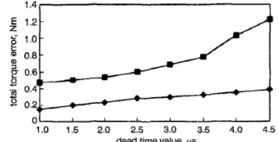
Figs. 15 and 16 show the torque error AT, against dead time duration and switching frequency without and with dead time effect compensation, respectively. The torque command is set as 2" and the load torque value is set as 0. )Observing Figs. 15 and 16, dif- ferent dead times produce various values of torque error. Similar to Figs. 8 and 9, the same trend of dead time duration effects can be observed. Comparing Figs. 15 and 16, it can be observed that a torque error of Fig. 16 is always smallix than that of Fig. 15, espe- cially in higher switching frequency regions. This fact can also be further illusmated by Fig.
17,
which shows the total torque error of different switching frequencies under different dead time durations. From Fig. 17, the total torque error of the compensated controller under each dead time duration is always smaller than that of the uncompensated controller.IEE Proc.-Electr. Power Appl., Vol. 145, No. 4 , July 1998
Fig. 18 shows the simulated resuIt of the desired, actual and estimated phase
a
voltage Vas while applying the proposed method on a direct torque controller. Similarly to that in Fig. 11, the actual voltage is equal to the estimated voltage and is different from the desired voltage. This will also verify the correctness of the proposed method.1.0 1.5 2.0 2.5 3.0 3.5 4.0 4.5 dead time value, ps
Fig. 17
ferent dead time durations Total torque error of dflerent switching frrquencies under d$
0 (i) 200 (ii) (iii) -200 200 - -200 200 -200 I
-
0.501 time, s 0.5Fig. 18 Comparison of desired, estimated and actual voltage V,, From the above description, it can easily be con- cluded that dead time effects will certainly deteriorate the performance of controllers, especially under some extreme conditions. In applications where high per- formance is needed, it is thus desirable to perform the proposed dead time effect compensation method to obtain a better result.
4 Conclusions
A novel dead time compensation mlethod is proposed in this paper. The proposed method can calculate a more accurate output voltage using a simple equation and then compensate the dead time effect by slight modification of the controller software. The proposed method is suitable for all controllers which utilise space vector modulation techniques.
In this paper, the proposed method is applied to two kinds of motor control applications: dead time effects under uncompensated and compensated conditions are analysed. Three major advantages can be achieved: Dead time effects can be greatly reduced utilising the proposed method. In sensorless vector control applica- tions, the speed error under different dead time dura- tions can be reduced by
-
0.25-0.6. In direct torque control applications, the torque error under different dead time durations can be reduced by-
0.6-0.67. Only slight modification of the controller software is required, and thus no additional hardware is needed inthis method.
The equation used to calculate the real output voltage is very simple, and therefore the proposed method can effectively improve the controller performance without degrading its operating speed.
Nevertheless, there are some potential disadvantages. First, the equation used to calculate the real output voltages is derived from a space vector concept; this method is not suitable for application
not
using space vector modulation techniques. The second is that only dead time effect is considered in this approach; other switching device characteristics such as turn on/off time and voltage drop effect have not been taken into con- sideration.However, owing to its remarkable simplicity and evi- dent performance improvement, the proposed method offers an attractive choice for dead time compensation.
References
BROECK, H W , SKUDELNY, H C , and STANKE, G V ‘Analysis and realisation of a pulsewidth modulator based on voltage space vectors’, IEEE Trans, 1988, IA-24, (l), pp 142-149
KUBOTA, H , MATSUSE, K , and NAKANO, T ‘DSP-based speed adaptive flux observer of induction motor’, IEEE Trans KIM, Y R SUL, S K , and PARK, M H ‘Speed sensorless vec- tor control of induction motor using extended Kalman filter’,
IEEE Trans, 1994, 1A-30, (5), pp 1225-1233
TAKAHASHI, I , and NOGUCHI, T ‘A new quick-response and high-efficiency control strategy of an induction motor’, IEEE
T f u n s
1993, IA-29, (2), pp 344348
1986, IA-22, (5), pp 820-827
5 HABETLET, T.G., PROFUMO, F., PASTORELLI, M., and TOLBERT, L.M.: ‘Direct torque control of induction machines using space vector modulation’, IEEE Trans., 1986, IA-28, ( 5 ) ,
6 CHOI, J.W.: ‘Inverter output voltage synthesis using novel dead time compensation’, IEEE Trans., 1996, P C l l , (2), pp. 221-227
SUI, T., and OKUYAMA, T.: ‘Fully digital, vector-controlled PWM VSI-fed ac drives with an inverter dead-time compensation strategy’, IEEE Trans., 1991, IA-27, (3), pp. 552-559
8 LEGGATE, D., and KERKMAN, R.J.: ‘Pulse-based dead-time compensator for PWM voltage inverters’, IEEE Tvans., 1997, I C
44, (2), pp. 191-197
MIKI, I., NAKAO, O., and NISHIYAMA, S.: ‘A new simplified current control method for field-oriented induction motor drives’,
ZEEE Trans., 1991, IA-27, (6), pp. 1045-1053
pp. 1045-1053
7 SUKEGAWA, T., KAMIYAMA, K., MIZUNO, K., MAT-
9
6 Appendix: Motor parameters
The parameters of 3hp motor are as follows:
rs (stator resistance) = 2.7Q
r,. (rotor resistance) = 2.23Q L, (stator self-inductance) = 352mH
L, (rotor self-inductance) = 352mH
L, (statorhotor mutual inductance) = 342.SmH J, (inertia of rotor) = 0.0082SNm2
B (damping coefficient) = 0.0001 Nm2