Photoluminescence of InAs
0.04P
0.67Sb
0.29 Gene Tsai, De-Lun Wang, and Hao-Hsiung Lina兲Graduate Institute of Electronics Engineering and Department of Electrical Engineering, National Taiwan University, Taipei 10617, Taiwan
共Received 3 March 2008; accepted 22 May 2008; published online 30 July 2008兲
We report the results of a detailed photoluminescence共PL兲 study on quaternary InAs0.04P0.67Sb0.29 grown by gas-source molecular-beam epitaxy. The main PL peak at 10 K shows a transition energy that is lower than the calculated energy gap by 0.223 eV, which is attributed to the tail states recombination. Another PL band, which emerges as the temperature increases, is assigned to the self-activated luminescence from defect centers. Its features, namely, nearly temperature-independent peak energy, Gaussian-like lineshape, and square-root-of-temperature-dependent linewidth, can be illustrated by the configuration coordinate model. The vibration energy, calculated from the linewidth at low temperature, is 0.022 eV for the excited state of the defect centers. The self-activated luminescence shows a thermal quenching behavior that is usually exhibited by amorphous semiconductors, indicating that the defects are related to the compositional disorder. The defects responsible for the luminescence are most likely complexes consisting of a substitutional carbon and an In vacancy. © 2008 American Institute of Physics. 关DOI:10.1063/1.2960504兴
I. INTRODUCTION
Midinfrared共MIR兲 emitters covering the 2–4 m spec-tral range have attracted much attention due to their promis-ing applications in gas sensing or free-space communications.1,2 Previous studies revealed that InAsPSb quaternary lattice matched with InAs is a useful alloy for MIR emitters.3,4 However, a miscibility gap共MG兲 exists in the low-As side of InAsPSb, which limits the growth range and the usefulness of this alloy.5Several works reported the growth of high-quality InAsPSb alloys with compositions close to the MG boundary by using liquid-phase epitaxy. The lowest As mole fraction achieved in these reports was⬃0.36, along with the successful demonstration of 2.5 m light-emitting diodes.6 Metal-organic chemical vapor deposition and molecular beam epitaxy 共MBE兲 are commonly consid-ered to be far from thermal equilibrium. Their capability of growing InAsPSb lying deeply in the MG region have been demonstrated.7–9 In this respect, many studies were focused on the material growth of InPSb. Its application to the clad-ding layers of MIR laser devices was also reported.8 How-ever, a systematic investigation into the optical properties of low-As InAsPSb is still required. So far, the most important finding on this issue is that the transition energy of the pho-toluminescence 共PL兲 is much lower than the energy gap, which is due to the strong compositional disorder in the alloys.7,9 In this paper, we report a detailed study on the PL of an InAs0.04P0.67Sb0.29 bulk layer. In addition to the band tail luminescence resulting from the compositional disorder, we observed self-activated luminescence. The luminescence shows a Gaussian-like lineshape, temperature-independent peak energy, and a linewidth proportional to the square root of the temperature. The intensity shows a temperature depen-dence that is usually exhibited by amorphous
semiconduc-tors, revealing that the defects are related to the composi-tional disorder. The origins of the luminescence are most likely due to complexes consisting of a substitutional carbon and an In vacancy.
II. EXPERIMENTAL PROCEDURES
A VG-V80H gas-source MBE 共GSMBE兲 system was used to grow 1-m-thick InAs0.04P0.67Sb0.29 on a 共100兲 n-type InAs substrate. Pure arsine 共AsH3兲 and phosphine 共PH3兲, the precursors of the two group-V gas sources, were cracked in a gas cell at 1000 ° C to provide the As2and P2 beams for the epitaxy process. A mixed beam of Sb2and Sb was supplied by a cracking effusion cell 共EPI Inc.兲. A con-ventional thermal effusion cell was employed as the group-III 共In兲 source. The beam fluxes of the Sb and In sources were calibrated using an ion gauge, while those of the As and P sources were controlled by the gas pressures of the arsine and phosphine in the manifolds behind the microleaks of the gas cell. The growth temperature was set at 470 ° C and the growth rate was kept at 1 m/h. After the growth, a JEOL JXA-8200 electron probe microanalyzer was used to quan-tify the composition of the InAsPSb epilayers. InAs, InP, and InSb binary substrates were used as standards for ZAF cor-rection. PL measurements were carried out using a SPEX 500M monochromator calibrated by the radiation lines of a Xe lamp. The sample under test was excited by a 532 nm diode-pumped solid-state laser. The luminescence was first dispersed by the monochromator and then collected by a liquid-nitrogen-cooled InSb detector. In order to prevent the atmospheric absorption, particularly the absorption by water vapor at 2.7 m, in this work, CaF2 lenses and windows were used and nitrogen gas was used to purge the optical path and the monochromator.
a兲Electronic mail: [email protected].
III. RESULTS AND DISCUSSIONS
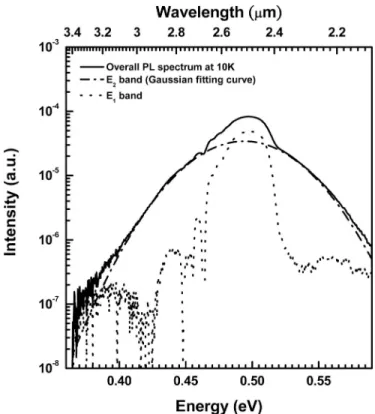
The composition of the studied sample, a 1-m-thick InAs0.04P0.67Sb0.29 epilayer grown at 470 ° C, lies deeply in-side the MG region. Its detailed structural properties have been previously reported and indicate that the sample suffers from strong compositional disorder.9 Figure 1 shows the temperature-dependent PL spectra with the temperature rang-ing from 10 to 250 K. The excitation power was 100 W/cm2. As can be seen in the figure, when the tempera-ture exceeds 170 K, the luminescence shows a single broad-band with a Gaussian-like lineshape. The dip in the emission spectrum at 0.45− 0.46 eV is due to the absorption of light by water vapor. However, as the temperature is further de-creased, a bump gradually rises from the low-energy shoul-der of the broadband and finally dominates the luminescence at 10 K. The bump and the broadband are hereafter referred to as E1and E2, respectively. In order to discern E1from E2, we used a Gaussian function to fit E2and then recovered the lineshape of E1by subtracting the fitting curve from the mea-sured spectrum. The results are shown in Fig.2. As we can see, the Gaussian fitting is reasonably good. The recovered E1band shows dips in its low-energy tail, which are due to the absorption of light by water vapor and measurement er-rors. The peak energies of these two bands are then plotted against the temperature in Fig.3. For comparison, the theo-retically calculated energy gap as a function of temperature is also depicted 共dashed line兲. The calculation considered three binary energy gaps10 and the bowing parameters of InAsSb,11InAsP,11and InPSb.7We assumed that the bowing parameters are temperature independent. The peak energy of the E1band redshifts from 0.5 to 0.44 eV as the temperature increases from 10 to 130 K, while the peak energy of E2is virtually fixed at 0.49 eV throughout the whole temperature range. Both peak energies are far below the calculated en-ergy gap, as can be seen in the figure. The enen-ergy difference between E1and the calculated energy gap at 10 K is as large
as 0.223 eV. A similar phenomenon has been reported in literatures8 and was attributed to deep tail states resulting from compositional disorder.
Here, we ascribe the E1band to the recombination of the
FIG. 1. Temperature-dependent PL spectra of InAs0.04P0.67Sb0.29. The
tem-perature range is 10–250 K. Peak E1redshifts as the temperature increases.
Above 90 K, peak E2dominates the spectrum; its peak energy is
indepen-dent of temperature.
FIG. 2. Lineshape fitting for the 10 K PL spectrum. The overall spectrum can be decomposed into two bands. The broader E2band was obtained by
Gaussian fitting and is attributed to deep-level transition. The stronger E1
band was obtained by deducting the E2curve from the overall spectrum and
is attributed to tail state transition. The dips around 0.45− 0.46 eV in E1
band are due to the absorption of light by water vapor, which is not consid-ered in the Gaussian fitting. The deviation of the overall spectrum from the Gaussian fitting below the intensity level of 10–6may have resulted from the
measurement error and background noise.
FIG. 3. PL transition energies as functions of temperature. Dashed line is the calculated band gap. The energy difference between the energy gap and E1
carriers trapped in the deep tail states on the basis of the following observations. First, the E1 band has a slow low-energy tail at 10 K, which is a feature of luminescence from tail states. Second, the peak energy is far below the calcu-lated energy gap and agrees with the aforementioned findings in literatures.7 Moreover, we also performed power-dependent PL measurements at 10 K. The peak energy of the E1 band retrieved from the overall spectrum shows a blue-shift with increasing excitation power. Because of the low density of the band tail states, an increment in carrier density leads to filling of these states and results in the observed blueshift in the emission energy. The third observation is that the peak energy redshifts slightly faster than the calculated energy gap as the temperature increases, which indicates that the E1 band is relevant to the energy bands. The faster slope is probably due to thermally assisted tunneling between the localized tail states. This tunneling process would allow the transition of carriers to lower energy states as the tempera-ture increases and thus lead to a faster redshift. However, as we can see in Fig. 1, the increment in temperature also re-sults in the diminishing intensity of the E1band. This implies that the carriers trapped in the tail states escape due to the thermal energy. Since the band edge luminescence at the calculated energy was not observed simultaneously, the es-caping carriers are most likely recaptured by nonradiative centers either through extended bands or the tunneling pro-cess.
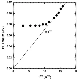
Because of its Gaussian-like lineshape, we attributed the E2 band to the luminescence from a deep-level transition. Here, we use the configuration coordinate 共CC兲 model to illustrate this recombination process.12,13 The model is gen-erally applied to the defects with strong electron-phonon coupling. In such defects, the wave function of a trapped carrier is localized at a specific bond, and this asymmetrical distribution would induce the atoms to shift from their origin sites. After recombination, the atoms relax through lattice vibrations, i.e., the phonon emission process. Due to the parabolic nature of the energy versus position relation of lattice vibrations, the deep-level transition has a Gaussian-like lineshape, which is just the observed feature of the E2 band. As can be seen in Fig.3, the transition energy of the E2 band is nearly independent of the temperature. This indicates that the luminescence is associated with a moleculelike de-fect center. If a dede-fect center is sufficiently localized, the thermally induced lattice expansion and vibrations would al-most exert no influence on its behavior; consequently, its luminescence peak energy would exhibit a negligible shift with temperature. This behavior has been reported in litera-tures and explained successfully by the CC model.13To fur-ther confirm that the luminescence is from a defect, we in-spect the temperature evolution of the full width at half maximum 共FWHM兲 shown in Fig. 4. The FWHM derived from the CC model is given by
W = W0关coth共h/2kT兲兴1/2, 共1兲
where h is the energy of the vibration mode of the excited state, kT is the thermal energy, and W0is the FWHM at 0 K, which is due to the minimum energy in quantum harmonic oscillators and can be expressed as follows:14
W0=共8S ln 2兲1/2h, 共2兲
where S is the Huang–Rhys factor, which represents the mean number of phonon emissions. As can be seen in Fig.4, the FWHM of the E2 band satisfies Eq. 共1兲 quite well. At high temperature, the FWHM is proportional to the square root of temperature. As the temperature is lower than 100 K, the FWHM saturates at 0.08 eV. From Fig. 4, one can find that hv = 0.022 eV, W0= 0.08 eV, and S = 2.8. The vibration energy of 0.022 eV is smaller but close to the energies of InSb-like longitudinal optical共LO兲 phonons in InPSb that is lattice-matched to InAs共0.024 eV兲.15 The small energy dif-ference between the vibration mode and the InSb-like LO phonon mode of the host lattice implies that the Coulomb field induced by the defect charge has a slight effect on the lattice vibration, which explains the small Huang–Rhys factor.16
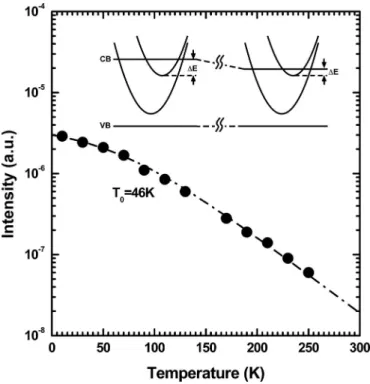
Figure5shows the integrated intensity of the E2band as a function of temperature. Here, instead of the Arrhenius plot, we adopt a formula, which has been used to consider
the thermal quenching process in amorphous
semiconductors,17 for the relation between the PL intensity IPLand temperature T,
IPL=
B 1 + A exp共T/T0兲
, 共3兲
where T0 is the characteristic temperature; A and B are con-stants. As can be seen, the equation is a fairly good fit to the integrated PL intensity with a characteristic temperature T0 of 46 K. As the temperature increases, the local vibrations of the defect centers increase and eventually liberate the elec-trons in the excited states to the conduction band where they are lost by a nonradiative recombination process. Due to the compositional disorder in the sample, the defect centers at different locations have different activation energies, as shown in the inset of Fig. 5. Therefore, luminescence FIG. 4. FWHM of the PL band E2of InAs0.04P0.67Sb0.29as a function of the
square root of temperature. In the high temperature range, FWHM fits the dashed line, indicating that it is proportional to the square root of temperature.
quenching becomes a collective behavior of defect centers with different activation energies. Such a situation is similar to the conditions considered in the model proposed by Col-lins and Paul18for amorphous Si:H, in which they suggested a distribution that represents the number of radiative centers with an activation energy of E,
g共E兲 ⬀ exp共–E/E0兲, 共4兲
where E0= kT0ln共C兲 and C is a constant relevant to the non-radiative recombination process. Here, because the change in activation energy is due to the composition fluctuation, E0is relevant to the variation in the conduction band seen by the defect centers. Reihlen et al.7 estimated E0 in InPSb from below band edge absorption measurements. Their results were within 50− 60 meV, much larger than kT0⬃4 meV observed in this work. However, the absorption measure-ments were performed over the entire epilayer and hence correspond to the undulation of the energy gap of the entire sample. In contrast, the characteristic temperature T0 ob-served from the quenching process in this study only repre-sents the variation in the conduction band seen by the de-fects. Therefore, the large discrepancy between the results of Reihlen et al.7and our results indicates that the defect cen-ters are not uniformly distributed in the sample but concen-trated in the potential wells resulting from the compositional disorder. The localization of the defects in a low-potential region may reduce the slope of the energy distribution seen by the defects, i.e., E0 in Eq.共4兲. Such a defect distribution
implies that the defect centers could be generated by the compositional disorder.
The deep levels responsible for the E2band are possibly due to vacancy-impurity complexes. The nearly temperature-independent behavior of the E2peak energy suggests that the band is from a moleculelike center, which implies that both the ground and excited states should be within the energy gap. Pötz and Ferry19 have calculated the defect levels in III-V semiconductors using a rescaled defect-molecule model. However, the results for vacancies and antisites in InAs, InP, and InSb indicate that a single isolated defect can-not meet the requirements. We believe that the defect center is most likely composed of a substitutional carbon and an In vacancy, i.e., a VIn– CAs or VIn– CIn complex. Carbon is a common residual impurity in MBE-grown compound semi-conductors. A few reports observed a carbon-related vibra-tion gap mode at 220 cm–1 in carbon-doped InP grown by GSMBE and chemical beam epitaxy.20,21 The vibration en-ergy of this mode is close to that of our sample. Moreover, in a previous study, Williams and Bebb14 observed the self-activated luminescence from a VGa– CAscomplex in GaAs. The reported vibration energy is also 0.022 eV.12 Interest-ingly, the difference between the peak energy of VGa– CAs complex and the energy gap is ⬃0.3 eV. Therefore, we at-tribute the E2band to the luminescence from complexes that consist of a substitutional carbon and an In vacancy. How-ever, further research is required to understand the origin of the observed deep-level transition in InAsPSb.
IV. CONCLUSION
We report the results of a detailed PL study on an InAs0.04P0.67Sb0.29 epilayer grown on an InAs substrate by GSMBE. Two PL bands were observed. The first one, domi-nant at 10 K, is attributed to the recombination of carriers trapped in the tail states resulting from compositional disor-der. Its peak energy is lower than the calculated energy gap by 0.223 eV, indicating strong disorder in the alloy. Another PL band with Gaussian-like lineshape, dominant at higher temperature, is ascribed to a deep-level transition because its luminescence behaviors coincide with the signature of the CC model. The transition energy fixed at⬃0.5 eV is virtu-ally temperature independent. The vibration energy for the excited state is calculated from the linewidth and is 0.022 eV. The PL intensity shows a thermal quenching behavior that is usually exhibited by amorphous Si:H, revealing that the lu-minescence center is related to the compositional disorder. We believe that the origins of the luminescence are com-plexes consisting of a substitutional carbon and an In va-cancy.
ACKNOWLEDGMENTS
This work was supported by the National Science Coun-cil of Taiwan under Grant No. NSC96-2221-E-002-279-MY3.
1J. Wagner, C. H. Mann, M. Rattunde, and G. Weimann,Appl. Phys. A: Mater. Sci. Process.78, 505共2004兲.
2M. Yin, A. Krier, S. Krier, R. Jones, and P. Carrington, Proc. SPIE 6399,
63990C共2006兲. FIG. 5. Integrated PL intensity of the deep-level band E2as a function of
temperature. Dashed line is the best fit of equation IPL= B/关1
+ A exp共T/T0兲兴, which is used to describe the quenching behavior of
amor-phous semiconductors. The inset shows the schematic CC diagrams of two defect centers at different locations. Due to the composition fluctuation, the defects see different conduction band edges and thus have different activa-tion energies. The equaactiva-tion represents a collective quenching behavior of a group of defect centers with different activation energies.
3N. Kobayashi and Y. Horikoshi, Jpn. J. Appl. Phys. 19, L641共1980兲. 4H. Mani, E. Tournie, J. L. Lazzari, C. Alibert, and A. Joullie,J. Cryst.
Growth121, 463共1992兲.
5T. Fukui and Y. Horikoshi, Jpn. J. Appl. Phys. 20, 587共1981兲. 6A. Krier and Y. Mao,IEE Proc.: Optoelectron.144, 355共1997兲. 7E. H. Reihlen, M. J. Jou, Z. M. Fang, and G. B. Stringfellow,J. Appl.
Phys.68, 4604共1990兲.
8R. M. Biefeld, K. C. Baucom, S. R. Kurtz, and D. M. Follstaedt,J. Cryst. Growth133, 38共1993兲.
9G. Tsai, D. L. Wang, C. E. Wu, C. J. Wu, Y. T. Lin, and H. H. Lin, J. Cryst.
Growth 301–302, 134共2007兲.
10V. Swaminathan and A. T. Macrander, Materials Aspects of GaAs and InP Based Structures共Prentice-Hall, New Jersey, 1991兲, p. 10.
11M. P. C. M. Krijn,Semicond. Sci. Technol.6, 27共1991兲. 12F. E. Williams and M. H. Hebb,Phys. Rev.84, 1181共1951兲.
13S. Shionoya, T. Koda, K. Era, and H. Fujiwara,J. Phys. Soc. Jpn.19, 1157
共1964兲.
14E. W. Williams and H. B. Bebb, in Semiconductors and Semimetals, edited
by R. K. Willardson and A. C. Beer共Academic, New York, 1972兲, Vol. 8, p. 370.
15D. Drews, A. Schneider, T. Werninghaus, A. Behres, M. Heuken, K.
He-ime, and D. R. T. Zahn, Appl. Surf. Sci. 123-124, 746共1998兲.
16K. Huang and A. Ruys,Proc. R. Soc. London, Ser. A204, 406共1950兲. 17R. A. Street, T. M. Searle, and I. G. Austin, in Amorphous and Liquid
Semiconductors, edited by J. Stuke and W. Brenig 共Taylor & Francis,
London, 1974兲, p. 953.
18R. W. Collins and W. Paul,Phys. Rev. B25, 5257共1982兲. 19W. Pötz and D. K. Ferry,Phys. Rev. B31, 968共1985兲.
20M. Ramsteiner, P. Kleinert, K. H. Ploog, J. Oh, M. Konagai, and Y.
Taka-hashi,Appl. Phys. Lett.67, 647共1995兲.
21J. H. Oh, J. Shirakashi, F. Fukuchi, M. Konagai, T. Azuma, and K.
Taka-hashi, Proceedings of the Indium Phosphide Related Materials, 1995 共un-published兲, p. 797.