Controlled Growth of Nanofiber Network Hole Collection Layers with Pore Structure for
Polymer-Fullerene Solar Cells
Jen-Hsien Huang,† Zhong-Yo Ho,‡ Dhananjay Kekuda,§Chih-Wei Chu,*,§,⊥and Kuo-Chuan Ho*,†,‡
Department of Chemical Engineering, National Taiwan UniVersity, Taipei, Taiwan 10617, Institute of Polymer Science and Engineering, National Taiwan UniVersity, Taipei, Taiwan 10617, Department of Photonics, National Chiao-Tung UniVersity, Hsinchu, Taiwan 30010 and Research Center for Applied Sciences, Academia Sinica, Taipei, Taiwan 11529
ReceiVed: May 13, 2008; ReVised Manuscript ReceiVed: October 5, 2008
In this study, we compare a series of hole collector layers (HCLs) with pore structure fabricated via an electrochemical method to construct polymer-fullerene solar cells. The HCLs with a pore structure can offer a large interface to enhance hole collection; however, the series resistances are also increased by the relatively pore morphology. Photovoltaic device with the largest short circuit current (Jsc) and efficiency is achieved
using poly(3,4-propylenedioxythiophene) (PProDoT) as HCLs due to its highly porous structure and reasonable series resistance. By further optimizing the thickness of the HCLs in the solar cell, a power efficiency of 3.57% under simulated sun light is achieved.
Introduction
Recently, solar cells as a promising source of renewable and truly clean energy have become more and more attractive. Since solution processed bulk heterojunction (BHJ) solar cells were first reported in the mid-1990s,1they have been the subject of
intense research interests due to their processing advantage as well as the superior mechanical properties of the polymers, such as flexibility. In such system, electron donors and acceptors are blended to form an interpenetrating network, providing a large interface area for the dissociation of excitons into free charges. Among polymer photovoltaic devices, the most promising candidate to date is blends of conjugated polymer as donor and soluble fullerene derivative as acceptor. Although several literatures have reported high performance solar cells using regioregular poly(3-hexylthiophene) (RR-P3HT) and [6,6]-phenyl C61-butyric acid methyl ester (PCBM),2-5 for the
polymer photovoltaic devices, it has long been regarded that the poor charge carrier transporters and short exciton diffusion length of polymers mainly limit the power conversion efficien-cies (PCE).
Several approaches have been proposed to enhance the performance of the RR-P3HT:PCBM system, including thermal and electrical annealing,6-10solvent annealing,11and microwave
annealing.12These annealing processes not only create a vertical
phase separation which helps the transfer of charges toward the respective electrodes but also enhances the ordered structure formation resulting a higher absorption and carrier mobility. Although the performance of the photovoltaic devices can be enhanced significantly via different annealing processes, the electron mobility in pristine PCBM (µe ) 2 × 10⁻⁷ m2V-1
s-1)13is found to be about one orders of magnitude higher than
the hole mobility measured in the pristine RR-P3HT (µh) 3 ×
10-8m2V-1s-1).14,15On the basis of these results, it is noticed
that the charge transport in RR-P3HT:PCBM solar cells is strongly unbalanced, and the photocurrent is expected to be limited by the build up of space-charge at the interface. Efficiency is largely limited by such unbalance charge transport, moreover, it also limited by the short exciton diffusion lengths (about 5-10 nm) of the active layers.16,17In practice, the charge
collection in the fine-scale blends is significantly smaller than the film thickness. As a result, when thick films were employed for the fabrication of the devices, the charges cannot find a pathway toward the electrode which will eventually recombine within the film, leading to a reduction in short circuit currents, which in turn reduces the efficiency of the devices. However, to achieve a highly efficient photovoltaic device, solar radiation needs to be efficiently absorbed by the active layers, for which the device thickness needs to be increased. At the same time there should be minimal recombination centers, which would probably increase the short circuit currents.
In view of the above-mentioned factors, in this work, we use 3,4-ethylenedioxythiophene (EDOT) and its derivatives to fabricate a highly porous hole collector layer (HCL) in nanoscale via the electrochemical deposition method, instead of using commercial poly(ethylene dioxythiophene) doped with poly-styrene sulfonic acid (PEDOT:PSS). Subsequently, the RR-P3HT:PCBM blending layer can be infiltrated into the porous HCL. This not only can increase the hole collection rate to reduce the unbalance charge transport within the device but also increase the effective thickness leading to a higher absorption without charge recombination.
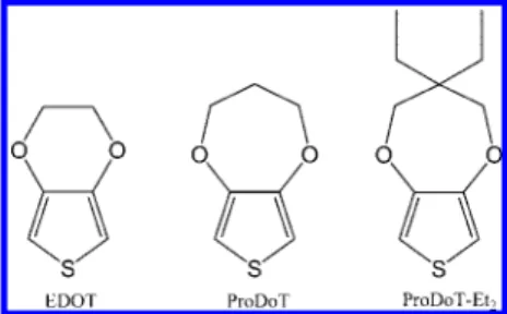
The chemical structures of EDOT, 3,4-propylenediox-ythiophene (ProDoT), and diethyl-3,4-dihydro-2H-thieno[3,4-b] [1,4]dioxepine (ProDoT-Et2) are shown in Scheme 1.The
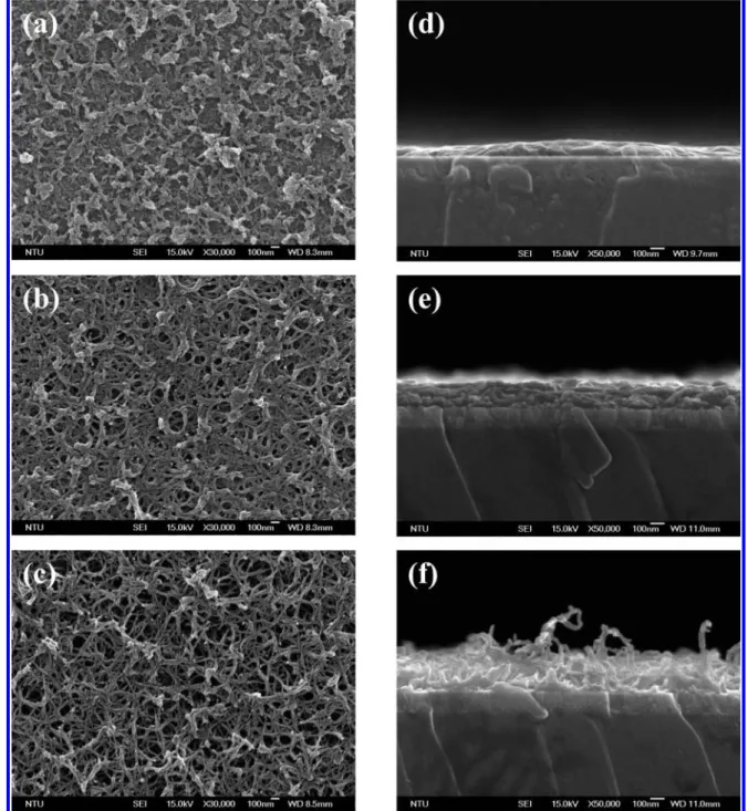
SEM topographic images of PEDOT, PProDoT, and PProDoT-Et2are shown in Figure 1a-c, respectively. These films were
prepared via electrochemical deposition by applying a potential at 1.1 V (vs Ag/Ag+(acetonitrile)) with a charge capacity of 5 * To whom correspondence should be addressed. (K.-C.H.) E-mail:
[email protected]. Telephone: +886-2-23660739. Fax: +886-2-23623040. (C.-W.C.) E-mail: [email protected]. Telephone: +886-2-27898000 ext 70. Fax: +886-2-27826680.
†Department of Chemical Engineering, National Taiwan University ‡Institute of Polymer Science and Engineering, National Taiwan
University
§Research Center for Applied Sciences, Academia Sinica ⊥Department of Photonics, National Chiao-Tung University
10.1021/jp804221u CCC: $40.75 2008 American Chemical Society Published on Web 11/07/2008
mC/cm2. The morphologies of the PEDOT and its derivatives
become more and more porous with increased ring size or attaching the carbon side chains. When the ring size is increased from two to three carbons (PEDOT to PProDoT), the coplanar stacking becomes weaker due to the larger twisty angle of the ring, resulting a nanofiber-shaped morphology. In the case of PProDoT-Et2, the highly porous morphology of PProDoT-Et2
is contributed from the ethyl subsititution to be positioned above and below the plane of the π-congugated backbone which represses π-stacking. Consequently, the crystallized structure of PEDOT or PProDoT contributed from the intermolecular interactions between oxygen and the adjacent thienyl hydrogen is destroyed, leading to a more porous film. The diameters of the nanofiber-shaped films are about 10-20 nm which forms a network HCL. The highly porous film can offer a large interface between the active layer and HCL leading a higher hole transfer rate, consequently a more balanced charge transport can be expected. The cross sectional SEM images of PEDOT, PProDoT and PProDoT-Et2are shown in Figure 1d-f, respectively. It
can be observed that there are two interfaces, namely the glass substrate/indium tin oxide (ITO) and the ITO/polymer film. The film thicknesses of PEDOT, PProDoT, and PProDoT-Et2 are
found around 100, 150, and 250 nm, respectively. Although these polymer films were fabricated under the same conditions, the film thicknesses become larger and larger with a looser structure. The thicknesses of the HCLs with various deposited charge density (Qd) are shown in the Supporting Information.
Table 1 shows the performance parameters (PCE, open-circuit voltage (VOC), JSC, fill factor (FF) and series resistance) of the
photovoltaic devices based on RR-P3HT:PCBM as a function of different HCLs (PEDOT, PProDoT, and PProDoT-Et2)
deposited at 2 mC/cm2. The thicknesses of PEDOT, PProDoT,
and PProDoT-Et2deposited at 2 mC/cm2 are 44, 59, and 97
nm, respectively. The series resistance of the devices was calculated from the I-V curves under dark current. The series resistance is given by the offset from linearity at high bias of the current-voltage characteristic.18The results indicate that
the device performance depends strongly on the morphological properties of the HCL. By comparing the performance param-eters of the devices, we see that the PProDoT system leads to the best device performance. Although PProDoT-Et2film, which
possesses the highest porosity, is expected to collect photocur-rent more efficiently, the series resistance of PProDoT-Et2(43.4
Ω) is larger than those of PEDOT and PProDoT. Hence, the devices with PProDoT-Et2layer exhibited lower current density
compared to those of PProDoT based devices. The larger resistance results from the poorπ-stacking leading to a loose bound structure which significantly increases the series resis-tance. In the case of PProDoT, the films exhibited relatively high porosity with a lower series resistance (31.8Ω), therefore a larger PCE was obtained. Although the thicknesses of these films are quite large, it should be noticed that the series resistances are still on the same order of magnitude as that of
the extremely thin PEDOT:PSS (20 nm) film reported previ-ously.19This is contributed from chemical composition of the
PEDOT and its derivatives prepared via electrodeposition. The commercial PEDOT:PSS, which contains nonconductive poly-mer segments of PSS, limits the conductivity significantly. However in this work, the PEDOT is doped with ClO4-,
therefore the PEDOT chains can still stack densely with doping of small anions leading to a highly conductive polymer film.20
Figure 2 shows the absorption spectra measured for PEDOT, PProDoT, and PProDoT-Et2deposited at 5 mC/cm2. Although
PEDOT reveals a larger absorbance than those of PProDoT and PProDoT-Et2, the spectra are all very similar and these films
are very transparent. The transmittance spectra of these films indicated that the transparency is higher than 75% (including ITO substrate) in the visible region (data not shown here). It is well-known that PEDOT and its derivatives are researched for their electrochromic properties.21,22They are cathodically
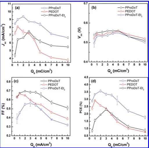
color-ing polymers that are dark opaque blue in their reduced state and become very transmissive light blue in their oxidized form. Even though their thicknesses are quite large according to the SEM images (larger than 100 nm), the films are very transparent as these polymer films were prepared under 1.1 V (vs Ag/Ag+) which is quite an oxidative potential (bleached state). Hence this photovoltaic device can be operated under light illumination without obviously absorbing by the HCLs at such film thicknesses. Figure 3 shows the performance parameters of the measured devices, namely JSC, VOC, FF, and PCE as a function of the
deposited charge density (Qd), made with three HCLs. In these
cases the measured values of JSC, FF, and PCE show an increase
and then decrease with a larger Qd. The best device performance
was obtained at Qd) 2 mC/cm2, and the values were JSC)
9.40 mA/cm2, FF ) 0.70, and PCE ) 3.57% for PProDoT as
the HCL. It is worthy to note that the optimal charge densities of PEDOT, PProDoT, and PProDoT-Et2are found to be 1, 2,
and 3 mC/cm2, respectively. And their film thicknesses are 25,
59, and 137 nm, respectively. From these data, it implies that the penetration depth of P3HT:PCBM is dependent on the morphology of the pore structure. The RR-P3HT:PCBM can be infiltrated into the porous PProDoT and PProDoT-ET2films
to increase the hole transport interface and the effective thickness of the active layer. This can increase the JSCand PCE as shown
in Figure 3. However the measured values of VOCincreased
gradually with the increase in Qd. In practice, the
electrodepo-sition mechanism of EDOT is divided into two stages.23The
initial stage of the eletrodeposition is the nucleation stage which forms PEDOT islands. In this stage, just a discontinuous polymer phase can be formed. In the latter stages, layer-by-layer growth mode was observed to form a continuous film. Hence, continuous HCLs can not be formed with a small Qd.
This causes a direct contact between RR-P3HT:PCBM and ITO substrate and results in a decrease of VOC. However, a thicker
film will increase the series resistance, and its influence on the Rsof the devices is listed in Table 2. As can be seen in Table
2, if the Qd increases further, the Rs increases significantly.
Therefore the JSC, FF, and VOCall decrease with larger Qdwhich
also leads to a poor PCE. It is worthy to note the device with PProDoT HCL shows a larger JSCand FF compared with the
case in PEDOT device although the Rsis larger in the case of
PProDoT. This can be interpreted by the fact that the higher hole collection in the porous PProDoT structure results in a more balanced charge mobility. The further Supporting Information of the electron and hole mobilities is shown in the Supporting Information.
SCHEME 1: Chemical Structures of PEDOT, PProDoT, and PProDoT-Et2
In order to prove that the P3HT:PCBM blend infiltrates into the porous HCLs, we apply X-ray photoelectron spectroscopy (XPS) for chemical analysis with a mixture of high-energy C60+
ions and low-energy Ar+ions gun.24,25With this cosputtering
technique, the chemical states of organics were preserved while a steady sputtering rate was achieved and the probing depth
Figure 1. SEM micrographs of PEDOT and its derivative films (a) PEDOT, (b) PProDOT, and (c) PProDOT-Et2. The cross sectional images of PEDOT and its derivatives films (d) PEDOT, (e) PProDOT, and (f) PProDOT-Et2.
TABLE 1: Performance of Parameters, Indicating PCE,
VOC, JSC, FF, and Series Resistance, for Solar Cells Made with PEDOT, PProDoT, and PProDoT-Et2as Hole HCLs Which Were Deposited at 2 mC/cm2
HCL[a] PCE (%) V OC(V) Jsc(mA/cm2) FF series resistance (Ω) PEDOT 2.58 0.53 7.41 0.65 28.7 PProDoT 3.57 0.55 9.40 0.70 31.8 PProDoT-Et2 1.94 0.53 6.68 0.55 43.4
aAll HCLs were deposited at 2 mC/cm2.
Figure 2. Absorption spectra of pristine films of PEDOT, PProDoT,
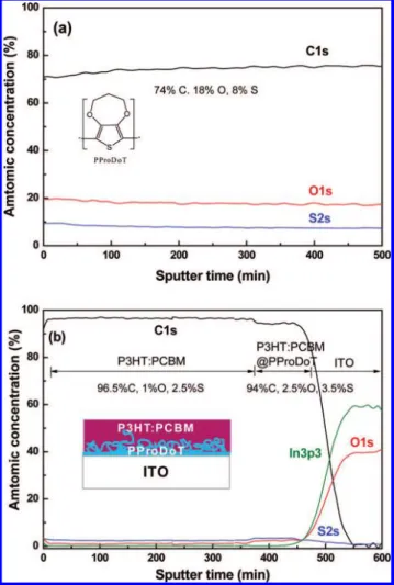
increased dramatically. Figure 4a shows the sputter depth profile of a PProDoT film. The chemical composition is expected to be 70% C, 20% O, and 10% S. Although the measured C is slightly high (74%), the composition is still very close to the expected. In the other hand, the solar cell device with PProDoT as HCL was also investigated with the XPS using C60as ion
guns. The depth profile shows the P3HT:PCBM layer (96.5% C, 1% O, and 2.5% S) between 0 and 370 min, the mixed P3HT: PCBM and PProDoT layer (94% C, 2.5% O, and 3.5% S) between 370 to 450 min and the transparent ITO electrode after 450 min. The composition of P3HT:PCBM active layer is in good agreement with the previous report.24Note that the O and
S concentration increases from 1 to 2.5% and 2.5 to 3.5%, respectively, in the P3HT:PCBM-PProDoT layer between 370 to 450 min. The change in composition is due to the infiltration of P3HT:PCBM into the PProDoT layer and produce a composition(94% S, 2.5% O, and 3.5% S) neither P3HT:PCBM nor PProDoT. Therefore the results offer a further Supporting
Information for the P3HT:PCBM infiltrates into the porous structure of PProDoT.
Figure 5 shows the J-V characteristics in the dark and under illumination for the as-fabricated device using PProDoT as the HCL deposited at 2 mC/cm2and the device with the commercial
PEDOT:PSS. Although the device fabricated with PEDOT:PSS shows a larger VOC(0.6 V) however the PCE is still lower due
to its lower JSC(8.93 mA/cm2) and FF (0.61) compared with
the one based on PProDoT as HCL. The larger FF and JSCof
the device with PProDoT are contributed from the higher conductivity. The commercial PEDOT:PSS, which contains nonconductive polymer segments of PSS, limits the conductivity significantly. However in this work, the PProDoT is doped withClO4-, therefore the PProDoT chains can still stack densely
with doping of small anions leading to a highly conductive polymer film. Furthermore the PProDoT with porous structure promoting the hole collection which leads to a more balanced charge mobility. Hence the FF and JSCare larger than the one
of the device based on PEDOT:PSS. Furthermore, the PProDoT device shows a good diode behavior in the dark with a rectification factor close to 1000 ((1 V) and a very low leakage current as shown in the insert of Figure 5.
In conclusion, we have fabricated photovoltaic cells based on RR-P3HT:PCBM with the PEDOT and its derivatives as the HCLs. The present results demonstrate that improved photovoltaic performance can be achieved with PEDOT and its derivatives prepared via electrochemical polymerization. The PProDoT system shows light-harvesting properties superior to those of PEDOT and PProDoT-Et2. The highly porous and low
series resistance of PProDoT make it an ideal HCL for photovoltaic devices. As a result, PCE of the devices based on
Figure 3. JSC, VOC, FF, and PCE plotted as a function of the electrodeposited charge density for PEDOT, PProDoT, and PProDoT-Et2. TABLE 2: Series Resistance Calculated from I-V Plots in
the Dark for the Solar Cells with Different Qd
series resistance, Rs(Ω)
deposited charge
density (mC/cm2) PEDOT PProDoT PProDoT-Et 2 0.5 21.8 27.7 29.8 1.0 25.9 29.4 38.9 2.0 28.7 31.8 43.4 3.0 30.7 33.4 55.4 4.0 33.2 37.4 78.9 5.0 36.6 39.8 84.4 7.0 44.5 46.8 97.6 10.0 56.9 60.3 127.8
PProDoT can reach as high as 3.57%. Furthermore, the simple and cheaper synthesis of HCLs makes the large area process possible for industrial production.
Experimental Section
Before device fabrication, a layer of PEDOT or its derivatives was electrochemically deposited to modify the ITO surface. The monomers EDOT, ProDoT, and ProDoT-Et2 were purchased
from Aldrich (97%). The electrodeposition procedures were used according to literature.26The electrochemical depositions of the
PEDOT and its derivatives were carried out in a three-electrode electrochemical cell with a platinum foil counter electrode and Ag/Ag+ reference electrode (0.01 M AgNO3 and 0.1 M
TBAClO4 in acetonitrile). Optically transparent ITO glass
substrates (Rsh) 15 Ω/sq.) were used as the working electrode.
The ITO glasses (1.5 × 1.5 cm2) were ultrasonically cleaned
in Triton X-100, deionized water, acetone and isopropyl alcohol before the deposition. After routine solvent cleaning, the substrates were treated with UV ozone for 15 min. The monomer solution contained 0.01 M EDOT or its derivatives in 0.1 M LiClO4/boron trifluoride-ethyl ether solution. The deposition of
PEDOT was controlled by an Autolab potentiostat/galvanostat (Eco Chemie, model PGSTAT30). The PEDOT thin films were electropolymerized onto the ITO glass substrates by applying a potential at 1.1 V (vs Ag/Ag+) to pass the predetermined amounts of charge density.
The polymer photovoltaic devices were fabricated by spin-coating blend of RR-P3HT:PCBM on the PEDOT modified ITO surface. The RR-P3HT was purchased from Rieke Metals. The regioregularity, weight (Mw), number (Mn) average molecular
weights, and polydispersity index (PDI) of RR-P3HT are as follows: regioregularity ) 93% Mw) 3.7 × 10⁴, Mn) 2.5 ×
104, and PDI ) 1.48, respectively. The PCBM was purchased
from Nano-C. Prior to the deposition, the blend of RR-P3HT: PCBM was prepared by dissolving it in 1,2-dichlorobenzene with 1:1 weight ratio, followed by stirring the solution for 12 h at 50°C. The active layer was obtained by spin-coated the blend at 600 rpm for 60 s. The active layer was then dried in covered Petri glass dishes. Subsequently, the films were annealed on the top of hotplate at 130°C. A 30 and 100 nm thick layer of calcium and aluminum, respectively, was thermally evaporated under vacuum at a pressure below 6 × 10⁻⁶ Torr through a shadow mask. The active area of the device was controlled at 0.12 cm2. Testing was done under simulated AM 1.5G
irradia-tion at 100 mW/cm2using a xenon lamp based solar simulator
(Thermal Oriel 1000W). The light intensity was calibrated by a monosilicon photodiode with KG-5 color filter (Hamamatsu, Inc.). The whole measurement was performed in a glovebox filled with N2at room temperature. XPS spectra were recorded
on a PHI 5000 VersaProbe (ULVAC-PHI, Chigasaki, Japan) system using a microfocused (100µm, 25 W) Al X-ray beam with a photoelectron takeoff angle of 45°. A dual-beam charge neutralizer (7 V Ar+ and 30 V electron beam) was used to compensate the charge-up effect. The Ar+ion source (FIG-5CE) was operated at various energies using a floating voltage of 500 V. The beam current was adjusted by the strength of the condenser lens. The beam was rastered on an area of 2 mm× 2 mm at an incident angle of 45°. A Wienfiltered C60+ion source
(IOG C60-10, Ionoptika, Chandler’s Ford, U.K.) was operated at 10 nA and 10 kV, with rastering on an area of 2 mm× 2 mm at an incident angle of 70° (70°from the normal to the surface for analysis). The angle between the Ar+and C60+ion
beam was 33°. The ion-beam current was measured with the target current of an Au foil. The base pressure of the main chamber (<1 × 10⁻⁷ Pa) was achieved by evacuation using turbomolecular and ion-getter pumps.
Acknowledgment. The authors are grateful to the National
Science Council (NSC), Taiwan (NSC 97-2120-M-002-012 and NSC 96-2221-E-001-017-MY2), and Academia Sinica for financial support.
Figure 4. XPS depth profile of (a) PProDoT layer. (b) Photovoltaic
device with PProDoT as HCL using 10 kV, 10 nA C60+mixed with a
0.2 kV, 300 Na Ar+beam.
Figure 5. J-V curves for P3HT:PCBM with PProDoT and PEDOT:
PSS as the HCL in the dark and under illumination. The inset shows the device based on PProDoT in the dark and under illumination in the semilogarithmic plot.
Supporting Information Available: The experimental for
extracting the hole and electron mobility and the summary of film thickness for the HCLs with various Qd.. This material is
available free of charge via the Internet at http://pubs.acs.org.
References and Notes
(1) Yu, G.; Gao, J.; Hummelen, J. C.; Wudl, F.; Hegeer, A. J. Science
1995, 270, 1789.
(2) Camaioni, N.; Ridolfi, G.; Casalbore-Miceli, G.; Possamai, G.; Maggini, M. AdV. Mater. 2002, 14, 1735.
(3) Moule´, A. J.; Allard, S.; Kronenberg, N. M.; Tsami, A.; Scherf, U.; Meerholz, K. J. Phys. Chem. C 2008, 112, 12583.
(4) Reyes, M.; Kim, K.; Carroll, D. L. Appl. Phys. Lett. 2005, 87, 083506.
(5) Kim, Y.; Choulis, S. A.; Nelson, J.; Bradley, D. D. C. Appl. Phys.
Lett. 2005, 86, 063502.
(6) Padinger, F.; Rittberger, R. S.; Sariciftci, R. S. AdV. Funct. Mater.
2003, 13, 85.
(7) Pandey, A. K.; Nunzi, J. M.; Wang, H.; Oey, C. C.; Djurisˇiæ, A. B.; Xie, M. H.; Leung, Y. H.; Man, K. K. Y.; Chan, W. K. Org. Electron.
2007, 8, 396.
(8) Yang, X.; Loos, J.; Veenstra, S. C.; Verhees, W. J. H.; Wienk, M. M.; Kroon, J. M.; Michels, M. A. J.; Janssen, R. A. J. Nano Lett. 2005,
5, 579.
(9) Ma, W.; Yang, C.; Gong, X.; Lee, K.; Heeger, A. J. AdV. Funct.
Mater. 2005, 15, 1617.
(10) Dante, M.; Peet, J.; Nguyen, T. Q. J. Phys. Chem. C 2008, 112, 7241.
(11) Li, G.; Shrotriya, V.; Huang, J.; Yao, Y.; Mariarty, T.; Emery, K.; Yang, Y. Nat. Mater. 2005, 4, 864.
(12) Ko, C. J.; Lin, J. K.; Chen, F. C. AdV. Mater. 2007, 19, 3520. (13) Mihailetchi, V.; Van Duren, J. K. J.; Blom, P. W. M.; Hummelen, J. C.; Janssen, R. A. J.; Kroon, J. M.; Rispens, M. T.; Verhees, W. J. H.; Wienk, M. M. AdV. Funct. Mater 2003, 13, 43.
(14) Goh, C.; Kline, R. J.; McGehee, M. D.; Kadnikova, E. N.; Frechet, J. M. J. Appl. Phys. Lett. 2005, 86, 122110.
(15) Mozer, A. J.; Sariciftci, S. N. Chem. Phys. Lett. 2004, 389, 438. (16) Theander, M.; Yartsev, A.; Zigmantas, D.; Sundstro¨m, V.; Mammo, W.; Andersson, M. R.; Ingana¨s, O. Phys. ReV. B 2000, 61, 12957.
(17) Kroeze, J. E.; Savenije, T. J.; Vermeulen, M. J. W.; Warman, J. M.
J. Phys. Chem. B 2003, 107, 7696.
(18) Chirvase, D.; Parisi, J.; Hummelen, J. C.; Dyakonov, V.
Nano-technology 2004, 15, 1317.
(19) Li, G.; Shrotriya, V.; Yao, Y.; Yang, Y. J. Appl. Phys. 2005, 98, 043704.
(20) Kumar, A.; Welsh, D. M.; Morvant, M. C.; Piroux, F.; Abboud, K. A.; Reynolds, J. R. Chem. Mater. 1998, 10, 896.
(21) Welsh, D. M.; Kumar, A.; Meijer, E. W.; Reynolds, J. R. AdV.
Mater. 1999, 11, 1379.
(22) Groenendaal, L. B.; Zotti, G.; Aubert, P. H.; Waybright, S. M.; Reynolds, J. R. AdV. Mater. 2003, 15, 855.
(23) Randriamahazaka, H.; Noe¨l, V.; Chevrot, C. J. Electroanal. Chem.
1999, 472, 103.
(24) Yu, B. Y.; Chen, Y. Y.; Wang, W. B.; Hsu, M. F.; Tsai, S. P.; Lin, W. C.; Lin, Y. C.; Jou, J. H.; Chu, C. W.; Shyue, J. J. Anal. Chem. 2008,
80, 3412.
(25) Chen, Y. Y.; Yu, B. Y.; Wang, W. B.; Hsu, M. F.; Lin, W. C.; Lin, Y. C.; Jou, J. H.; Shyue, J. J. Anal. Chem. 2008, 80, 501.
(26) Shi, G. Q.; Jin, S.; Xue, G.; Li, C. Science 1995, 267, 994. JP804221U