On the enhancement of field emission performance of ultrananocrystalline diamond
coated nanoemitters
Yu-Fen Tzeng, Yen-Chih Lee, Chi-Young Lee, I.-Nan Lin, and Hsin-Tien Chiu
Citation: Applied Physics Letters 91, 063117 (2007); doi: 10.1063/1.2768880 View online: http://dx.doi.org/10.1063/1.2768880
View Table of Contents: http://scitation.aip.org/content/aip/journal/apl/91/6?ver=pdfcov Published by the AIP Publishing
Articles you may be interested in
Ultrananocrystalline diamond nano-pillars synthesized by microwave plasma enhanced nucleation and bias-enhanced growth in hydrogen-diluted methane
J. Appl. Phys. 112, 124307 (2012); 10.1063/1.4769861
Enhanced electron field emission properties by tuning the microstructure of ultrananocrystalline diamond film J. Appl. Phys. 109, 033711 (2011); 10.1063/1.3544482
Growth, microstructure, and field-emission properties of synthesized diamond film on adamantane-coated silicon substrate by microwave plasma chemical vapor deposition
J. Appl. Phys. 107, 103305 (2010); 10.1063/1.3427436
Synthesis of single crystalline silicon nanowires and investigation of their electron field emission J. Vac. Sci. Technol. B 24, 20 (2006); 10.1116/1.2137338
Growth aspects of nanocrystalline diamond films and their effects on electron field emissions J. Vac. Sci. Technol. B 23, 786 (2005); 10.1116/1.1880112
This article is copyrighted as indicated in the article. Reuse of AIP content is subject to the terms at: http://scitation.aip.org/termsconditions. Downloaded to IP: 140.113.38.11 On: Thu, 01 May 2014 00:20:21
On the enhancement of field emission performance of ultrananocrystalline
diamond coated nanoemitters
Yu-Fen Tzeng and Yen-Chih Lee
Department of Materials Science and Engineering, National Tsing Hua University, 101, Sec. 2, Kuang-Fu Road, Hsinchu 30043, Taiwan, Republic of China
Chi-Young Leea兲
Center of Nanotechnology, Materials Science, and Microsystem, National Tsing Hua University, 101, Sec. 2, Kuang-Fu Road, Hsinchu 30043, Taiwan, Republic of China
I.-Nan Linb兲
Department of Physics, Tamkang University, 151 Ying-Chuan Rd., Tamsui 251, Taiwan, Republic of China
Hsin-Tien Chiuc兲
Department of Applied Chemistry, National Chiao Tung University, Hsinchu 30050, Taiwan, Republic of China
共Received 23 April 2007; accepted 16 July 2007; published online 8 August 2007兲
Ultrananocrystalline diamond 共UNCD兲 nanoemitters were synthesized by a microwave plasma enhanced chemical vapor deposition process using silicon nanowires 共SiNWs兲 as the template. Preseeding markedly enhances the nucleation of diamond on the SiNW templates, resulting in UNCD grains of smaller size and uniform distribution, which leads to significantly improved electron field emission 共EFE兲 properties. The EFE for UNCD nanoemitters can be turned on at 共E0兲UNCD-NE= 4.4 V /m, achieving large EFE current density, 共Je兲UNCD-NE= 13.9 mA/ cm2 at an
applied field of 12 V /m, which is comparable with that of carbon nanotubes, but with much better processing reliability. © 2007 American Institute of Physics.关DOI:10.1063/1.2768880兴
Diamond films have been extensively investigated for applications as electron field emitter in vacuum microelec-tronic devices owing to the negative electron affinity with low effective work functions.1,2 However, the electron field emission properties of these materials are inferior to those of carbon nanotubes due to the large electric field required for turning on the electron field emission process.3 How to re-duce the turn-on field for diamond films is thus urgently required. Several methods have been proposed to enhance the electron field emission properties of the diamond films,4–7 including the synthesis of aligned silicon tip arrays as templates for fabricating diamond emitters.7–9 However, conformal coating of diamond films on silicon nanowires 共SiNWs兲 is extremely difficult. In this letter, we grew ul-trananocrystalline diamond共UNCD兲 films on aligned SiNWs in order to synthesize UNCD nanoemitters that possess elec-tron field emission 共EFE兲 properties comparable with those of the carbon nanotubes but with markedly better processing reliability.
The SiNWs were fabricated by an electroless metal deposition 共EMD兲 process, which is described elsewhere.10 SiNWs were thus formed on the Si substrate via a self-aligned galvanic anisotropic etching process. Furthermore, some of the SiNWs were preseeded by ultrasonication in nanodiamond 共⬃30 nm兲 slurry for 30 min to facilitate the formation of diamond nuclei on the Si surface. UNCD films were deposited on either unseeded or preseeded SiNWs by microwave plasma enhanced chemical vapor deposition 共MPECVD兲 共IPLAS, Cyrannus兲 for 2 h under an Ar-plasma environment in which the gas flow was 1 and 99 SCCM 共SCCM denotes cubic centimeter per minute at STP兲 for
methane and argon respectively, and the total pressure was 100 torr. The microwave power was 600 W共2.45 GHz兲 and the substrate temperature was 673 K.
The morphologies of the SiNWs and diamond coated SiNWs were examined using scanning electron microscopy 共SEM兲 共JEOL JSM-6500F兲, whereas the crystal structure of these nanowires was investigated using high-resolution transmission electron microscopy 共TEM兲 共JEOL JEM-4000EX兲. The structure of the diamond coated SiNWs was examined by Raman spectroscopy共Renishaw, 632.8 nm兲 and near-edge x-ray absorption fine structure共NEXAFS兲 in syn-chrotron radiation. The EFE properties of the diamond coated SiNWs were measured with a tunable parallel plate setup, in which the sample-to-anode distance was varied us-ing a micrometer. The current-voltage 共I-V兲 characteristics were measured using an electrometer 共Keithley 237兲 under pressures below 10−6torr and were analyzed by the Fowler-Nordheim model.11
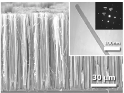
Figure1shows that well aligned SiNWs about 90m in
a兲FAX:⫹886-3-5166687; electronic mail: [email protected] b兲FAX:⫹886-2-26209917; electronic mail: [email protected] c兲FAX:⫹886-3-5723764; electronic mail: [email protected]
FIG. 1. SEM micrographs of SiNWs fabricated by EMD process using 共100兲 Si substrates. The inset shows the TEM micrograph of an independent SiNW and the corresponding SAD patterns.
APPLIED PHYSICS LETTERS 91, 063117共2007兲
0003-6951/2007/91共6兲/063117/3/$23.00 91, 063117-1 © 2007 American Institute of Physics
This article is copyrighted as indicated in the article. Reuse of AIP content is subject to the terms at: http://scitation.aip.org/termsconditions. Downloaded to IP: 140.113.38.11 On: Thu, 01 May 2014 00:20:21
length are uniformly formed on the Si substrates by the EMD process. The SiNWs formed bundles with diameters of hun-dreds of nanometers. The inset in Fig. 1 reveals that the SiNWs are about 35 nm in diameter and are关100兴 oriented. The UNCD films can grow directly on these SiNW templates even when they are not subjected to the seeding process. Such a growth behavior is markedly better than that of UNCD on planar Si substrates.12,13This result infers that the as-etched SiNWs surface already contains abundant active sites, which readily react with carbon species in the plasma, forming diamond nuclei. However, the coating of UNCD on these unseeded SiNWs is not uniform. In some areas, the UNCD grains fully cover the SiNWs, forming a continuous film, while in others only discrete and sparse UNCD grains are observed.
Figure 2共a兲 shows that the UNCD grains are densely coated on SiNWs, when they are preseeded. The TEM mi-crograph shown in Fig.2共b兲 indicates that the grain size of UNCD films obtained by this method is about 5 nm and the grain size distribution is very uniform. The selective area diffraction 共SAD兲 pattern in the inset of Fig. 2共b兲 demon-strates that the grains are diamonds. Most importantly, the UNCD grains conformably cover the SiNWs. Restated, the seeding process dramatically increases the density of dia-mond nuclei, resulting in conformal coating of diadia-mond
grains in SiNW templates. It should be noted that the param-eters in the seeding process are quite critical.
Typical NEXAF spectrum shown in Fig. 3, displays a sharp rise near 289.7 eV and a deep valley near 302.5 eV 共labeled as* band兲. These results confirm the sp3-bonded nature of the UNCD grains, which is in agreement with the SAD patterns observed in the TEM micrographs 关insets in Fig.2共b兲兴 and is strong evidence of the diamond structure. The Raman spectroscopy, shown as inset in Fig.3, is not able to unambiguously identify the characteristics of UNCD films, as the Raman peaks are too broad, which can be at-tributed to both the smallness of diamond grains and the formation of trans-polyacetylene surrounding the nanosized grains.14,15
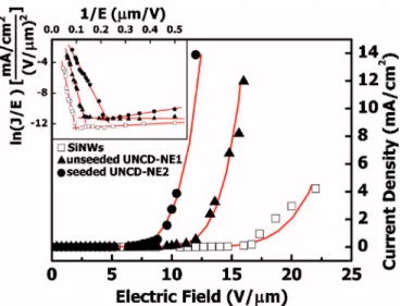
The EFE properties and the corresponding Fowler-Nordheim共F-N兲 plot of the SiNWs and UNCD nanoemitters are illustrated in Fig.4 and the corresponding inset, respec-tively. The important EFE parameters extracted from these J-E curves are listed in TableI. The turn-on field was desig-nated as the interceptions of straight lines extrapolated from the low-field and high-field segments of the F-N plots. The
FIG. 2.共a兲 SEM and 共b兲 TEM micrographs of UNCD nanoemitters fabri-cated on preseeded SiNWs by MPECVD process for 2 h. The inset in共b兲 shows the SAD patterns of UNCD films.
FIG. 3. Typical NEXAFS and Raman 共inset兲 spectra for UNCD nanoemitters.
FIG. 4. Electron field emission properties and current density–field共J-E兲 plots of SiNWs and UNCD nanoemitters, which were prepared on unseeded or preseeded SiNWs using the MPECVD process for 2 h共the insets are the corresponding Fowler-Nordheim plots兲.
063117-2 Tzeng et al. Appl. Phys. Lett. 91, 063117共2007兲
This article is copyrighted as indicated in the article. Reuse of AIP content is subject to the terms at: http://scitation.aip.org/termsconditions. Downloaded to IP: 140.113.38.11 On: Thu, 01 May 2014 00:20:21
SiNWs require a very large turn-on field, 共E0兲SiNW = 8.6 V /m, to induce EFE and can attain only 共Je兲SiNW
= 4.2 mA/ cm2 EFE current density at an applied field of 共Ea兲SiNW= 22.0 V /m 共open squares, Fig. 4兲, even though
they are nanosized and possess large field enhanced factors 共兲. The UNCD-NE1 共solid triangles, Fig. 4兲 possess better EFE properties than the bare SiNWs, 共E0兲UNCD-NE1 = 7.4 V /m and 共Je兲UNCD-NE1= 12.0 mA/ cm2 at 16 V /m.
However, the EFE properties of the UNCE-NE1 vary pro-nouncedly among different samples, which is presumably due to the inconsistency of the UNCD coverage on the SiNWs.
On the other hand, UNCD-NE2 shows markedly supe-rior EFE properties to the other two nanoemitters. The turn-on field is only共E0兲UNCD-NE2= 4.4 V /m and EFE den-sity is as large as共Je兲UNCD-NE2= 13.9 mA/ cm2 at 12 V /m.
It should be noted that the UNCD nanoemitters fabricated on unseeded SiNWs can only attain共Je兲UNCD-NE1= 0.5 mA/ cm2
and the SiNWs can reach only共Je兲SiNW= 0.01 mA/ cm2under
the same conditions. These EFE characteristics are summa-rized in TableIto illustrate the superiority of UNCD nanoe-mitters fabricated on seeded SiNWs over UNCD nanoemit-ters made on unseeded SiNWs, not to mention plain SiNWs. The work function 共兲 of the UNCD nanoemitters was evaluated using the Fowler-Nordheim model. We first fit the J-E curves with an exponential function to extract the preex-ponential and exponent constants in the F-N model, i.e., Eq.
J共E兲 = AE2exp
冋
− B 3/2E
册
, 共1兲where A⬅e3/ 162បt2共y0兲 and B⬅共4/3e兲共2m/ប2兲1/2共y0兲 and is the work function of the emitting material. The results of fitting are shown as solid curves in Fig.4, illustrat-ing that the electron field emission data fit the F-N model very well. Assuming that the work function of SiNWs is the same as that of planar silicon materials, i.e.,Si= 4.1 eV,16 the  value of SiNWs can be estimated from the effective work function共e=3/2/兲 of SiNWs, which is proportional
to the slope of F-N plots, and the result is 共兲Si= 367. The value of共兲Siobtained from this is higher than that of planar Si materials, but is much lower than thevalue expected for nanowires with such a large aspect ratio. Low value for SiNWs is presumably due to “screening effect” of too densely populated SiNWs. Simple calculation17 shows that the value is around 5000 for a nanowire of the geometry about 35⫻90 000 nm2. The screening factor is thus esti-mated to be around a = 0.07X. Coating UNCD on SiNWs
could markedly reduce the field enhancement factor 共 value兲 of the nanowires owing to the increase in diameter 共a factor of 0.3– 0.5X兲. However, large screening effect due to densely populated nanowires共a⬃0.07X兲 is expected to pre-dominate the effective field enhancement factor 共 value兲. The effectivevalue for the UNCD-coated SiNWs was thus assumed to be the same as that for uncoated ones. Therefore, the effective work function 共e=UNCD3/2 /兲 of the UNCD-NEs was again estimated from the slope of the corresponding F-N plots by assuming that 共兲UNCD-NEs=共兲SiNW= 367 for UNCD nanoemitters, and the work function of the UNCD nanoemitter was calculated to be 共兲UNCD-NE2= 2.23 eV, which is listed in TableI.
For the unseeded SiNWs, large UNCD clusters resulted due to fewer nuclei available and the SiNWs were not fully covered by UNCD grains. The electrons are most probably transported along the SiNWs and emitted from the tip, either through UNCD grains or the Si material. Therefore, the EFE current density is only moderately larger than that of SiNWs. In contrast, nucleation took place much more easily for the seeded SiNWs, resulting in densely populated UNCD grains on the SiNWs. The electrons are presumed to travel only through UNCD grains coated on SiNWs and are emitted at the tip of UNCD nanoemitters leading to a superior EFE current density compared to that of SiNWs.
In summary, UNCD nanoemitters were fabricated using MPECVD process with SiNWs as a template. TEM analysis indicates that UNCD nanoemitters are composed of 5 nm sized grains, which are uniformly distributed. SAD and NEXAF analyses confirm that the films coated on the SiNWs are diamonds. The denser granular structure markedly im-proves the EFE properties of the nanoemitters, which possess a turned-on field of共E0兲UNCD-NE2= 4.4 V /m and an electron field emission current density of 共Je兲UNCD-NE2
= 13.9 mA/ cm2at 12 V /m applied field.
1F. J. Himpsel, J. A. Knapp, J. A. VanVechten, and D. E. Eastman, Phys. Rev. B 20, 624共1979兲.
2W. Zhu, G. P. Kochanski, and S. Jin, Science 282, 1471共1998兲. 3Z. Xu, X. D. Bai, E. G. Wang, and Z. L. Wang, Appl. Phys. Lett. 87,
163106共2005兲.
4X. Lu, Q. Yang, W. Chen, C. Xiao, and A. Hirose, J. Vac. Sci. Technol. B 24, 2575共2006兲.
5K. Okano, S. Koizumi, S. R. P. Silva, and G. A. J. Amaratunga, Nature共London兲 381, 140 共1996兲.
6Z. L. Wang, Q. Luo, J. J. Li, Q. Wang, P. Xu, Z. Cui, and C. Z. Gu, Diamond Relat. Mater. 15, 631共2006兲.
7D. Zhou, A. R. Krauss, L. C. Qin, T. G. McCauley, D. M. Gruen, T. D. Corrigan, and R. P. H. Chang, J. Appl. Phys. 82, 4546共1997兲.
8J. Liu, V. V. Zhirnov, G. J. Wojak, A. F. Myers, W. B. Choi, J. J. Hren, S. D. Wolter, M. T. McClure, B. R. Stoner, and J. T. Glass, Appl. Phys. Lett.
65, 2842共1994兲.
9K. Q. Peng, Y. J. Yang, S. P. Gao, and J. Zhu, Adv. Mater.共Weinheim, Ger.兲 14, 1164 共2002兲.
10Y. F. Tzeng, K. H. Liu, Y. C. Lee, S. J. Lin, I. N. Lin, C. Y. Lee, and H. T. Chiu, Nanotechnology共in press兲.
11R. H. Fowler and L. W. Nordheim, Proc. R. Soc. London, Ser. A 119, 173 共1928兲.
12Y. C. Lee, S. J. Lin, I. N. Lin, and H. F. Cheng, J. Appl. Phys. 97, 054310 共2005兲.
13Y. C. Lee, S. J. Lin, D. Pradhan, and I. N. Lin, Diamond Relat. Mater. 15, 353共2006兲.
14C. Ferrari and J. Robertson, Phys. Rev. B 63, 121405共2001兲.
15R. J. Nemanich, J. T. Glass, G. Lucovsky, and R. E. Shroder, J. Vac. Sci. Technol. A 6, 1783共1988兲.
16M. Ding, H. Kim, and A. Akinwande, Appl. Phys. Lett. 75, 823共1999兲. 17E. I. Givargizov, V. V. Zhirnov, A. N. Stepanova, E. V. Rakova, A. N.
Kiselev, and P. S. Plekhanov, Appl. Surf. Sci. 87, 24共1995兲. TABLE I. Electron field emission properties of the SiNWs and UNCD
nanoemitters.
SiNWs UNCD-NE1 UNCD-NE2
Je共mA/cm2兲a ⬍0.01 0.5 13.9
E0共V/m兲b 8.6 7.4 4.4
⌽ 共eV兲c 4.10 3.43 2.23
aJ
eis the electron field emission current density achieved at 12.0 V /m
applied field. bE
0is the turn-on field estimated from Fowler-Nordheim plots, as the inter-ceptions of straight lines extrapolated from the low-field and high-field seg-ments of the F-N plots.
c is the work function and field enhancement factor deduced from J-E curves by using the F-N model.
063117-3 Tzeng et al. Appl. Phys. Lett. 91, 063117共2007兲
This article is copyrighted as indicated in the article. Reuse of AIP content is subject to the terms at: http://scitation.aip.org/termsconditions. Downloaded to IP: 140.113.38.11 On: Thu, 01 May 2014 00:20:21