國 立 交 通 大 學
光電工程研究所
博
士
論
文
三五族半導體發光元件結構優化之研究
Study of Structure Optimization in III-V
Semiconductor Light Emitting Devices
中 華 民 國 九 十 六 年 九 月
研 究 生: 張詒安
Student: Yi-An Chang
指導教授:
郭浩中 教授
王興宗 教授
Advisor:
Dr. Hao-Chung Kuo
Dr. Shing-Chung Wang
三五族半導體發光元件結構優化之研究
Study of Structure Optimization in III-V
Semiconductor Light Emitting Devices
研 究 生:張詒安 Student:Yi-An Chang
指導教授:郭浩中教授 Advisor: Dr. Hao-Chung Kuo
王興宗教授
Dr. Shing-Chung Wang
國 立 交 通 大 學 電機資訊學院
光電工程研究所
博 士 論 文
A dissertation
Submitted to Institute of Electro-Optical Engineering
College of Electrical Engineering and Computer Science
National Chiao Tung University
in partial Fulfillment of the Requirements
for the Degree of
Doctor of Philosophy
in
Electro-Optical Engineering
September 2007
Hsinchu, Taiwan, Republic of China
三五族半導體發光元件結構優化之研究
研究生:張詒安
指導教授:郭浩中教授
王興宗教授
國立交通大學光電工程研究所
摘要
本 論 文 旨 在 探 討 三 五 族 光 電 半 導 體 元 件 包 含 紫 外 線 發 光 二 極 體(ultraviolet light-emitting diode, LED)、紅光共振腔發光二極體(resonant-cavity LED)、850-nm面射 型雷射(vertical-cavity surface-emitting laser)以及1.3-µm側射型雷射(edge-emitting laser) 之操作性能改良相關研究。對於半導體發光元件而言要使其具有高輸出功率以及高穩 定性的輸出性能,元件磊晶晶體品質(epitaxial crystal quality)以及元件磊晶結構設計上 實屬於相當重要一環;其中要使發光元件能穩定地操作在高溫高輸入電流的情況下, 磊晶結構的設計更扮演極重要的角色。本論文即以有機金屬液相沉積法(metalorganic chemical vapor deposition, MOCVD)成長以上四種元件,配合理論模擬方式進行結構設 計上的改良來使電子能有效地被侷限於活性層量子井 (active region quantum well) 裡,達到降低電子溢流(electron leakage)提升元件輸出性能的目的。在紫外線發光二極體研究上,我們以四元氮化鋁鎵銦(AlGaInN)為活性層材料並 製做出最大輸出功率達4 mW,外部量子效率(external quantum efficiency)為1.2%,波 長為370 nm的發光二極體。而為使此一元件具有較高之輸出功率以及穩定的高溫高輸 入電流特性,我們以理論模擬方式進行元件結構的改良設計,探討氮化鋁鎵銦量子井 個數以及氮化鋁鎵電子阻礙層對元件輸出特性的影響。模擬結果顯示當氮化鋁鎵銦量 子井個數為五至七個和氮化鋁鎵電子阻礙層中鋁組成為19%時,可以達到降低電子溢 流作用並提供較佳之輸出特性。 在紅光共振腔發光二極體研究上,由於元件活性層量子井材料磷化鋁鎵銦
(AlGaInP)的導電帶能帶間隙值只有約300 meV,當電子注入量子井中很容易產生電子 溢流現象進而降低元件於高溫操作下的輸出性能。藉由將傳統共振腔發光二極體共振 腔長為一個波長增加為三個波長,我們發現在溫度範圍25–95ºC變化下,傳統結構在 注入電流固定為20 mA的輸出功率變化為-2.1 dB,而共振腔長為三個波長的共振腔發 光二極體卻只有-0.6 dB,且其遠場圖(far field pattern)隨注入電流變化相當穩定,適合 做為塑膠光纖傳輸的光主動元件。理論模擬結果也證明,增加共振腔長至三個波長亦 即增加量子井個數至三倍,確實有助於降低電子溢流達到侷限電子、穩定元件高溫、 高電流特性的目的。
在850-nm面射型雷射研究上,首先針對具有不同壓縮應力之量子井結構進行理論 分析,發現以具有較高壓縮應力值的砷化鋁鎵銦(AlGaInAs)做為量子井比起砷化銦鎵 (InGaAs)可以具有較高之材料增益(material gain) ,較低透明載子密度(transparency carrier concentration)與透明自發輻射電流密度(transparency radiative current density)。 接著我們選擇以Al0.08Ga0.77In0.15As做為量子井實際成長並做成元件,我們得到在室溫 操作下的850-nm面射型雷射,其臨界電流為1.47 mA,電光轉換效率(slope efficiency) 為0.37 mW/mA,且隨操作溫度升高至95 ºC,臨界電流值增加至2.17 mA,電光轉換效 率降為0.25 mW/mA。爲進一步改善雷射輸出性能,我們首次於活性層量子井中加入 一電子阻礙層,發現於室溫操做的850-nm面射型雷射臨界電流降低至1.33 mA,電光 轉換效率也達到0.53 mW/mA,且當溫度升高至95 ºC時臨界電流值只增加0.27 mA,電 光轉換效率也仍有0.4 mW/mA的表現。同時我們也以數值模擬方式證明加入電子阻礙 層確實可以有效阻擋電子溢流進而提升雷射輸出性能。 在1.3-µm InGaAsN/GaAsN側射型雷射研究上,由於實際成長氮砷化銦鎵磊晶結 構時,於砷化鎵位障層(barrier)裡加入氮可以平衡InGaAsN量子井裡的高壓縮應力 (compressive strain)並有助於避免量子井中氮原子的流失(out-diffusion),然而卻會因導 電 帶 能 帶 間 隙 值 降 低 而 產 生 電 子 溢 流 現 象 。 因 此 首 先 針 對 氮 砷 化 銦 鎵 (In0.4Ga0.6As0.986N0.014)單量子井旁的氮砷化鎵位障層進行理論模擬分析,探討氮砷化鎵 位障層中氮的成分對元件輸出性能的影響,我們提出以GaAs N 做為位障層,不
僅可以符合實際磊晶考量,更可防止電子溢流現象發生。經由實際磊晶成長及製程大 小為4×1000 µm2的雷射元件後,在室溫操作下此一元件的臨界電流值為84 mA,電光 轉換效率為9%;當操作溫度增加至105 ºC,臨界電流值增加至188 mA,特徵溫度 (characteristic temperature, T0)為118 K。為改善元件高溫高注入電流特性,我們更嘗試 於活性層量子井中加入磷砷化鎵(GaAs0.9P0.1)電子阻礙層,發現雖然於室溫下臨界電流 值 為99 mA , 但 當 操 作 溫 度 為 105 ºC時 臨 界 電 流 值 降 低 至 172 mA , 特 徵 溫 度 (characteristic temperature, T0)為155 K。模擬結果亦證實加入磷砷化鎵做為電子阻礙層 確實可以防止電子溢流,但卻也有電洞分布不均勻現象(hole inhomogeneity)產生而導 致在低溫及低電流操作下元件之臨界電流值增加。而為防止電子溢流現象發生,我們 更提出在磷砷化鎵電子阻礙層中增加磷成分至15–20%來得到較高特徵溫度值之雷射 元件。 總而言之,在本論文中我們嘗試在半導體發光元件,包含紫外線發光二極體、紅 光共振腔發光二極體、850-nm面射型雷射以及1.3-µm側射型雷射的磊晶結構上,設計 最佳化結構來防止電子溢流現象發生進而提升元件的操作性能。祈望這些觀念與經驗 未來能對元件磊晶者在結構設計上有所裨益。
Study of Structure Optimization in III-V
Semiconductor Light Emitting Devices
Student : Yi-An Chang
Advisor : Dr. Hao-Chung Kuo
Dr. Shing-Chung Wang
Institute of Electro-Optical EngineeringNational Chiao Tung University
Abstract
In this dissertation, the improvement in operation performance of III-V optoelectronic semiconductor light emitting devices, which include ultraviolet (UV) light-emitting diode (LED), 660-nm red resonant-cavity LED, 850-nm vertical-cavity surface-emitting laser (VCSEL), and 1.3-µm edge-emitting laser (EEL), were studied. The key technologies for semiconductor light emitting devices to possess better output performance and high operation stabilities are the epitaxial crystal quality and the design of epitaxial structure. Noteworthily, the structure design is more important if we were to have a stable output performance in high temperature and high injection current operation. By using the epitaxial technology – metalorganic chemical vapor deposition (MOCVD) to grow the structures and advanced simulation programs to give theoretical analysis, the operation performances of semiconductor light emitting devices are investigated and improved. Mainly, we focus on confining the electrons effectively in the quantum well (QW) active region to reduce the electronic leakage current so as to improve the output performances.
In the research of UV LED, to emit an emission wavelength of 370 nm, quaternary AlGaInN is utilized as QW material during the epitaxy of UV LED. The device after standard process as 300×300 µm2 size chip can provide a maximal output power of 4 mW
UV LED, we then theoretically investigate the effect of the number of QWs and the aluminum content in AlGaN electron-blocking layer on the UV LED output performance. After fitting in with the experimentally demonstrated output performance of UV LED, we find that the UV LED can provide a better output performance when the aluminum content in AlGaN electron-blocking layer is in a range of 19–21% and the AlGaInN QW number is in a range of 5–7.
In the research of 650-nm RCLED, it is known that the conduction band offset value in AlGaInP material QW active region is approximately 300 meV. When the device is under high temperature operation, the electron leakage problem may become more serious and consequently leading to the degradation of output performance. By means of widening the resonant cavity to a thickness of three wavelength (3 λ), the degree of power variation between 25 and 95 ºC for the device biased at 20 mA is apparently reduced from -2.1 dB for the standard structure design (1-λ cavity) to -0.6 dB. The current dependent far field patterns also show that the emission always takes place perfectly in the normal direction, which is suitable for plastic fiber data transmission. To optimize the RCLED structure, we continue numerically studying the structure dependent output performance by using an advanced simulation program. After fitting in with the experimentally demonstrated output performances of RCLEDs, we analyze the percentage of electron leakage current of the two structures, and we find that the stable temperature dependent output performance of 3-λ-cavity RCLED is attributed to the reduction of electron leakage current.
In the research of 850-nm VCSEL, we first theoretically investigate the gain-carrier characteristics of In0.02Ga0.98As and InAlGaAs QWs of variant In and Al compositions.
More compressive strain, caused by higher In and Al compositions in InAlGaAs QW, is found to provide higher material gain, lower transparency carrier concentration and transparency radiative current density over a temperature range of 25−95 ºC. Then we choose Al0.08Ga0.77In0.15As as QW material in the epitaxy of 850-nm VCSEL structure.
After standard oxidation confinement process, this device can provide a threshold current of 1.47 mA with a slope efficiency of 0.37 mW/mA at 25 ºC, and the threshold current increases to 2.17 mA with a slope efficiency reduction of 32% when the device temperature is raised to 95 °C. To improve the operation performance of 850-nm VCSEL, a 10-nm-thick Al0.75Ga0.25As electron-blocking layer is employed in the QW active region for
the first time, and the threshold current at 25 ºC is found reducing to 1.33 mA with an increment of slope efficiency to 0.53 mW/mA. When the device temperature raises to 95 °C, the threshold current increases by only 0.27 mA and the slope efficiency drops by only 24.5%. Numerical simulation is also done to analyze the effect of the electron-blocking layer on the output performance of 850-nm VCSEL, and the results show that the output performance is improved by the reduction of electron leakage current.
In the research of 1.3-µm InGaAsN/GaAsN EEL, there has been several works investigating using strain GaAsN as direct barrier. Using GaAsN in the epitaxial growth can balance the highly compressive strain in InGaAsN QW and reduce the phenomenon of nitrogen out-diffusion from the well. However, it is a small bandgap material system, which indicates that the electron leakage may become more serious if adding more nitrogen into GaAsN barrier. Therefore, in the first instance, the temperature effects on the optical gain properties of single In0.4Ga0.6As0.986N0.014 QW with GaAsN barrier of different
nitrogen compositions are studied for optimization. Theoretically, we suggest using GaAs0.995N0.005 as direct barrier can be a better choice with the considerations of epitaxial
growth and electron confinement. Then we choose In0.4Ga0.6As0.986N0.014/GaAs0.995N0.005 as
active region in the epitaxial growth of 1.3-µm EEL structure. After standard process as 4×100 µm2 size chip, this device can provide a threshold current of 84 mA with a slope
efficiency of 0.09 mW/mA. When the device temperature increases to 105 °C, the threshold current becomes 188 mA and a characteristic temperature value (T0) of 118 K is
In0.4Ga0.6As0.986N0.014/GaAs0.995N0.005 EEL, we also try to insert a GaAs0.9P0.1 layer as
electron blocking layer in the epitaxial growth of 1.3-µm EEL. The threshold current of the device at 25 °C becomes 99 mA and a slope efficiency of 0.11 mW/mA is obtained. The threshold current at 105 °C only increases to 172 mA with a T0 value of 155 K and the
reduction of slope efficiency becomes less. Numerical simulation is done to analyze the effect of the electron blocking layer on the output performance of 1.3-µm EEL. The results show that the electron leakage current is reduced with the use of a high-bandgap GaAs0.9P0.1 layer. Further theoretical simulation work of investigating the effect of
increasing the phosphide composition in GaAsP electron-blocking layer on the T0 value is
also done. And, we find that increasing the phosphide composition in GaAsP to 15–20% can provide a better T0 value.
In a summary, the III-V optoelectronic semiconductor light emitting devices, which include 370-nm UV LED, 660-nm RCLED, 850-nm VCSEL, and 1.3-µm EEL, are experimentally demonstrated and theoretically analyzed for a purpose of reducing the electron leakage current and thus improving the operation performance. We hope those all will turn into useful information in the design and epitaxy of optoelectronic semiconductor light emitting devices.
誌謝
博士論文的順利完成,首先要對辛苦指導我四年的郭浩中教授以及王興宗教 授致上我最深忱的敬意,因為他們的耐心指導,讓我可以快速且有效率地進入專 業領域並找到研究方向。在博士班求學過程中,不論是在專業的實務與經驗或學 理上探討,他們也總是能提供諸多寶貴建議與指導,讓我不至於在研究的道路上 產生迷思。也感謝交通大學光電所盧廷昌教授與張振雄教授、彰化師範大學物理 系所郭艷光教授、台灣大學電機工程學系彭隆瀚教授、成功大學電機工程學系張 守進教授以及光電所許進恭教授、提供的諸多寶貴建議與指導,讓論文內容可以 更加完善。 感謝禧通科技施江霖博士、賴利弘博士與賴利溫博士,由於他們豪邁無私的 個性首肯讓我以學生身分進入公司學習磊晶與製程技術,也讓我提早擁有社會市 場上的實戰經驗以及教導我如何扮演好一個研發人員的角色,同時也要感謝禧通 科技那群可愛的同事們,蔡睿彥博士、俊龍、怡宗、妙佳、佳勳、千慧、心馨、 育德、意蓉、佳萍、僑宴、琇圓、正斌、乾森,以及海德威電子謝文昇副總、Joe、 James、Lynn、Ricky,謝謝你們三年來的陪伴。在學校生活中,特別感謝黃根生 博士以及余長治、賴芳儀、張亞銜、薛道鴻學長姐們在學業、學術研究上的幫助 以及工作經驗上的分享,有他們的引導讓我更清楚明白未來道路的規劃。感謝博 士班同學志強、泓文、榮堂在課業及研究上一路相互扶持奮鬥與努力,以及學弟 妹們宗憲、德忠、裕鈞、傳煜、永龍、俊毅、國鋒、敏瑛、薏婷、文燈、永昌在 實驗量測上的協助。也感謝彰化師範大學物理與光電系所學弟妹們勝宏、俊榮、 秀芬、尚衛在程式運算與理論模擬分析上的幫忙。謝謝實驗室助理淑致、麗君在 行政上的幫忙,所辦黃小姐、許小姐、湯先生、劉小姐、崔小姐等在計畫及行政 作業上的幫忙。並感謝所有曾經幫助過我的良師益友們。 最後最該感謝的是我的家人--爸爸、媽媽以及哥哥與姐姐,還有女朋友 Jessica 以及她的家人們。有你們精神上的支持、體諒與實質生活上的幫忙、照顧,讓我 可以在沒有後顧之憂的情況下專心完成博士學業。謝謝你們!你們永遠是我的最 愛。也謝謝曾經幫過我的人!謝謝你們! 詒安 于 96 年 9 月 5 日 交通大學光電工程研究所Contents
Abstract (in Chinese) I
Abstract (in English) IV
Acknowledge VII Contents VIII
List of figures XI
List of tables XVI
Chapter 1 Introduction
1
1-1 Historical review of nitride based LEDs 3
1-1-1 Wurtzite GaN material properties 6
1-1-2 Band parameters 8
1-1-3 Spontaneous and piezoelectric polarizations 14
1-1-4 Band alignment discontinuity 15
1-2 Historical review of RCLEDs 17
1-2-1 RCLED design rules 18
1-2-2 RCLED applications 21
1-3 Historical review of semiconductors 23
1-3-1 VCSELs 28
1-4 Historical review of 1.3-µm InGaAsN EELs 35
References 43
Chapter 2 Physical and numerical models
53
2-1 Drift-diffusion model 53
2-2 Optical gain/absorption calculation for quantum well 56 2-3 Self-consistent carrier density in nitrides 59 2-4 Many-body Coulomb interaction in nitrides 60
2-5 Thermal effects 61
2-6 Specific models in APSYS 63
2-7 Specific models in LASTIP 64
2-8 Specific models in PICS-3D 65
References 66
Chapter 3 Ultraviolet AlGaInN/GaN LEDs
67
3-1 Literature survey 67
3-2 Device fabrication and characteristics 69
3-3 Theoretical analysis 72
References 80
Chapter 4 Temperature insensitive 660-nm RCLED
84
4-1 Fabricated device characteristics 85
4-2 Theoretical analysis 91
4-3 Summary 98 References 99
Chapter 5 850-nm InAlGaAs/GaAs VCSEL
102
5-1 Theoretical analysis on InGaAlAs QWs 103 5-2 Optical properties of fabricated QWs and device fabrication 109
5-3 Fabricated device characteristics 113
5-4 Theoretical analysis on devices’ characteristics 117
5-5 Summary 120 References 122
Chapter 6 1.3-
µ
m InGaAsN/GaAsN lasers
125
6-1 Method and numerical parameters 126
6-2 Optical gain properties of InGaAsN QW with GaAsN barriers 128
6-3 Fabricated device characteristics 131
6-4 Numerical analysis of InGaAsN/GaAsN laser characteristics 135
6-5 Summary 140 References 141
Chapter 7 Conclusion and future work
144
List of figures
Chapter 1
Figure 1.1 Lattice constant of semiconductor materials as a function of
their bandgap energy………... 4 Figure 1.2 (a) Wurtzite crystal with lattice constants c and a. (b) The unit
cell of wurtzite GaN crystal………... 8 Figure 1.3 Valence-band structure of wurtzite GaN………. 8 Figure 1.4 Band edges of conduction and valence bands………. 14 Figure 1.5 A schematic layer consequence of the RCLED device………… 17 Figure 1.6 Schematic illustration of a resonant cavity consisting of two
mirrors with reflectivity R1 and R2……….. 19
Figure 1.7 Optical mode density for (a) a short and (b) a long cavity. (c)
Spontaneous emission spectrum of an LED active region…….. 20 Figure 1.8 Attenuation of a PMMA step-index POF……… 22 Figure 1.9 MOST technique concepts in home and automotive
multimedia networking……….... 22
Figure 1.10 Band diagram of a p-n junction LD with triple-QWs
Illustrating carrier transport process……….... 24 Figure 1.11 Schematic illustration of (a) p-n junction, and (b)
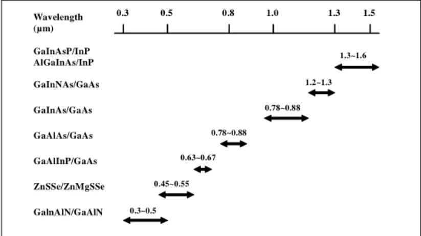
heterostructure lasers with their typical physical dimensions…. 24 Figure 1.12 Various choice of the active region material for different
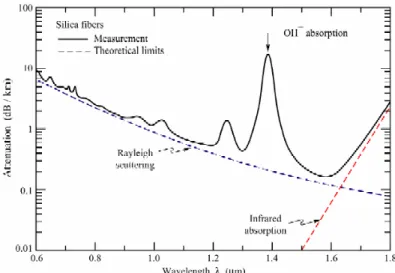
range of emission wavelength………. 25 Figure 1.13 Attenuation in silica fibers (solid line) and theoretical limits
(dash lines) given by Rayleigh scattering and molecular
vibration (infrared absorption)……… 26 Figure 1.14 (a) A schematic plot of the first room-temperature
continuous-wave operation red InGaP/InGaAlP
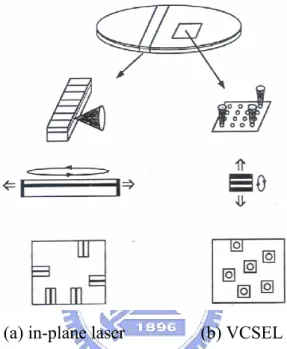
semiconductor laser. (b) is the lasing characteristic……… 27 Figure 1.15 Schematic illustrations of (a) an in-plane laser and
(b) a VCSEL……… 29
Figure 1.16 A schematic plot of a VCSEL epitaxial structure. The
reflectors are formed by DBRs with reflectivity above 99%... 30 Figure 1.17 Lasing modes of (a) an in-plane laser and (b) a VCSEL
change with the shift of gain spectrum………... 31 Figure 1.18 (a) Schematic illustration of the spectral misalignment between
threshold current dependence on the position across a wafer. (c) The VCSEL threshold current dependence on the device
temperature………. 32 Figure 1.19 Schematic representations of (a) air-post index guide (b)
Oxide confine index guide (c) implant confine gain guide
and (d) hybrid index and gain guide confine VCSELs………... 33 Figure 1.20 Bandgap energy of GaAs1-xNx as a function of nitrogen
composition. As shown the open squares are the experimental
data and the solid line is the theoretical calculation………….... 37 Figure 1.21 A schematic diagram of the band lineups for GaAsN,
InGaAs, and InGaAsN materials……… 38 Figure 1.22 A schematic diagram of GS-MBE growth apparatus…………. 40
Chapter 3
Figure 3.1 A schematic plot of the UV LED device………. 69 Figure 3.2 EL spectrum of the UV AlGaInN LED under
continuous-wave operation when the input current was
in a range of 10–100 mA………. 70 Figure 3.3 Output characteristics of the UV LED when the device
temperature was varied in a range of 300–380 K……… 71 Figure 3.4 Numerical spontaneous emission rate spectrum of the UV
AlGaInN LED as a function of the input current. The inset shows the main peaks of the numerical spontaneous
emission rate spectra and the experimental EL spectra……….. 74 Figure 3.5 Numerical temperature dependent output characteristics
of the UV AlGaInN LED……… 75 Figure 3.6 L-I characteristics of the UV AlGaInN LED with variant Al
compositions in AlGaN electron-block layer when the
device temperatures were 300 K and 380 K……… 76 Figure 3.7 Current efficiency of the UV AlGaInN LED as a function of
the input current for variant Al compositions in AlGaN electron-block layer when the device temperature were
300 K and 380 K………. 77
Figure 3.8 L-I characteristic of the UV AlGaInN LED with variant QW numbers when the device temperatures were
300 K and 380 K………. 78
Figure 3.9 Percentage of electron leakage current as a function of the device temperature when the QW number was in a range
of 1–11………. 79
Chapter 4
Figure 4.1 A schematic plot of device structure. Device A was designed with a conventional 1-λ resonant cavity. Device B was
designed to have a 3-λ resonant cavity, while the number
of QWs was tripled and separated into three parts……….. 86 Figure 4.2 Spectra of quantum well photoluminescence and reflectivity
of devices A and B………... 86 Figure 4.3 Temperature dependent L-I-V characteristic of the
fabricated (a) device A and (b) device B. The curve was
obtained in a device temperature range of 25–95 ºC…………... 88 Figure 4.4 Normalized external quantum efficiency (ηext) value obtained
at 20 mA with elevated device temperature from 25 to 95 ºC. The inset was the ηext value versus current at room
temperature for both devices………... 89 Figure 4.5 f-3 dB frequency bandwidth for devices A and B as a function
of bias current. The current aperture for both devices
A and B was 80 µm in diameter……….. 90 Figure 4.6 Evolution of far field patterns for both devices under room
temperature operation with increased bias current of 10–50 mA. The slightly unsymmetrical patterns could be
attributed to the TO package………... 91 Figure 4.7 Vertical profile of refractive index and optical intensity for
(a) device A and (b) device B……….. 94 Figure 4.8 Numerical results of temperature dependent L-I
characteristics of devices A and B………... 95 Figure 4.9 Vertical electron current distribution at 70 mA injection
current within the active regions of devices A and B………….. 96 Figure 4.10 Percentage of electronic leakage current as a function of the
bias current in devices A and B when the device
temperatures were 25 and 95 °C………. 97
Chapter 5
Figure 5.1 Calculated material gains of the In0.02Ga0.98As and InAlGaAs
QWs with Al0.3Ga0.7As barrier at 25 ºC when the input carrier
concentration is 6×1018 cm−3. The material gain tends to saturate when the Al composition in InAlGaAs QW is higher
than 8%... 105 Figure 5.2 Peak material gain as a function of (a) carrier concentration
and (b) radiative current density of the In0.02Ga0.98As and
InAlGaAs QWs with Al0.3Ga0.7As barrier at room
Temperature……… 106
Figure 5.3 Curves of valence band for the In0.02Ga0.98As and InAlGaAs
QWs with variant In and Al compositions at 25 ºC. The y axis
of the figures represents the valence band QW potential…….... 107 Figure 5.4 Calculated spectra of material gains of the In0.02Ga0.98As and
InAlGaAs QWs with Al0.3Ga0.7As barrier at 95 ºC when the
input carrier concentration is 6×1018 cm−3……….. 108 Figure 5.5 Peak material gain as a function of (a) carrier concentration
and (b) radiative current density of the In0.02Ga0.98As and
InAlGaAs QWs with Al0.3Ga0.7As barrier at 95 ºC………. 109
Figure 5.6 Temperature dependent PL peak emission wavelength of the In0.15Al0.08Ga0.77As triple-QW structure. The inset is
the optical spectrum obtained at 300 K………... 110 Figure 5.7 Normalized integrated PL intensity plotted as a function of
reciprocal temperature for the In0.15Al0.08Ga0.77As triple-QW
structure………... 111
Figure 5.8 A schematic plot of the VCSEL devices with and with a high
bandgap electron blocking layer………. 113 Figure 5.9 RT L-I-V characteristic of the fabricated VCSELs for devices
A, B, and C with an oxide aperture of 7 µm………... 114 Figure 5.10 Experimental temperature dependent variation of threshold
current and slope efficiency of devices A, B, and C…………... 115 Figure 5.11 RT relative intensity noise (RIN) value of the three devices
in a bias current range of 2–5 mA………... 116 Figure 5.12 Simulation results of the RT light output and voltage versus
current characteristics of devices A, B, and C. The electron blocking layers for devices B and C are 10-nm-thick
Al0.75Ga0.25As and 13-nm-thick Al0.9Ga0.1As, respectively……. 118
Figure 5.13 Expanded energy band diagram near the QW active region of device C. The diagram was obtained at RT with an
applied voltage of 2.1 V……….. 118 Figure 5.14 Percentage of electron leakage current as a function of input
current in device A when the device temperature was in
Figure 5.15 Percentage of electron leakage current as a function of device temperature for devices A, B, and C. The curves were
obtained when the devices were biased at 10 mA………... 120
Chapter 6
Figure 6.1 Calculated material gain of room-temperature
In0.4Ga0.6As0.986N0.014 and In0.8Ga0.2As0.69P0.31 quantum
wells when the input carrier concentration is 2×1018 cm-3……. 129 Figure 6.2 Maximum material gain of using GaAs1-xNx barriers with
x=0%, 0.5%, 1% and 2% as a function of temperature………... 129 Figure 6.3 Transparency carrier concentration as a function of
Temperature when using GaAs1-xNx barriers with
x=0%, 0.5%, 1% and 2%……… 130 Figure 6.4 A schematic diagram of the double-quantum-well
InGaAsN/GaAsN laser structure……… 133 Figure 6.5 Electroluminescence spectrum when the laser device was
at an input current of laser threshold……….. 133 Figure 6.6 Temperature dependent L–I characteristic of type A
laser under CW mode operation in a temperature
range of 25–105 ºC………. 134 Figure 6.7 Temperature dependent L–I characteristic of type B
laser under CW mode operation in a temperature
range of 25–105 ºC……….. 134 Figure 6.8 Threshold currents and slope efficiencies of type A and type
B lasers obtained experimentally and numerically………. 136 Figure 6.9 Room-temperature energy band diagrams of type A and type
B laser structures near the quantum well active region……….. 137 Figure 6.10 Percentage of electronic leakage current obtained
numerically as a function of device temperature for
type A and type B laser structures………... 138 Figure 6.11 Percentage of electronic leakage current of the laser structure
without GaAsP and with GaAsP current blocking layer of
P=10%–20% as a function of device temperature……….. 138 Figure 6.12 Numerical T0 value of the laser structure without GaAsP and
with GaAsP current blocking layer of P=10%–20%. The T0
List of tables
Chapter 1
Table 1.1 Band parameters of wurtzite binary GaN, AlN, and InN
alloys………... 10
Table 1.2 Valence band-offset values of wurtzite nitride binary alloys
(Unit: eV)……… 16
Chapter 3
Table 3.1 Net surface charge density at each interface of the UV LED….. 73
C
C
h
h
a
a
p
p
t
t
e
e
r
r
1
1
I
I
n
n
t
t
r
r
o
o
d
d
u
u
c
c
t
t
i
i
o
o
n
n
Since the first demonstration of high electroluminescence radiation from GaAs p-n junction in the early 1960s [1–5], compound semiconductors have functioned constantly in being promising materials in optoelectronic devices. So far, the optoelectronics has become an important part of our lives. Wherever converting current into optical signal or vice versa, the optoelectronic semiconductor devices all have a unique advantage, that is, they are tiny, and providing a high conversion efficiency that meets the steadily increasing mankind’s requirements. Examples include light-emitting diodes (LEDs) in illumination and other applications, photo-detectors in remote control sensors, and laser diodes (LDs) for digital disk storage system. While considering using the optoelectronic devices as active light sources, it is indubitably that group III-V compounds are the most excellent candidate because of their physically direct bandgap property. The devices such as LEDs, resonant-cavity light-emitting diodes (RCLEDs), edge-emitting laser diodes (EELDs), and vertical-cavity surface-emitting lasers (VCSELs) have been commercialized for several decades. These emitters can be used in the application of solid-state lighting, outdoor displays, laser pointer, printer, DVD players, and fiber communication etc. While selecting a suitable material to be the active media, a wide emission wavelength range covering untraviolet–blue–green–red–infrared region of the spectrum can be obtained. As an illustration, the devices made by GaN-based material can provide high efficient illumination in ultraviolet to green wavelength range and white emission. For high efficient yellow–red emission, the choice of the active media material grown on GaAs substrate is InGaP/InGaAlP. As extending the emission wavelength to infrared, the active media material can be InGaAlAs, InGaAsP, and InGaAsN.
environment colorful and brilliant. The unmitigated research efforts worldwide have resulted in making these emitters having better output performances. However, with an aim to improve the emitting power and efficiency of the semiconductor light emitting devices, substantial works are still needed. In which, further experimental demonstrations and theoretical simulation are both intensively required. The experiments facilitate the growth of high quality films that reduce the internal loss caused by the defects. The theoretical simulation can provide a more detailed understanding of device physics and simultaneously give a qualitative analysis to optimize the existed device structures. As these efforts continue, it is expected to enhance the output performances of the optoelectronic semiconductor devices.
In this dissertation, the improvement in operation performance of III-V optoelectronic semiconductor light emitting devices, which included UV-LED, 650-nm red RCLED, 850-nm VCSEL, and 1.3-µm EELD, were studied. The respective devices were fabricated. As well, in order to better understanding the device physics so as to improve the output performances, three advanced simulation programs developed by Crosslight Software, Inc. (APSYS, LASTIP, PICS3D) [6] were employed. Specifically, the physical discussion of reducing electronic leakage current in the fabricated devices was focused to improve the high temperature and high current injection device output performances. The following subsections in this chapter were intended to give an investigation and historical review of the nitride based LED, RCLED, and semiconductor lasers including EELD and VCSEL devices. The physical models in the software, regarding band structure calculation, drift-diffusion model, spontaneous and stimulated emissions, heat flux equations, and etc. were described in Chapter 2. Characteristics of the fabricated devices and the theoretical analysis were described in Chapters 3 to 6, respectively. Finally, conclusions were given in Chapter 7.
1-1 Historical review of nitride based LEDs
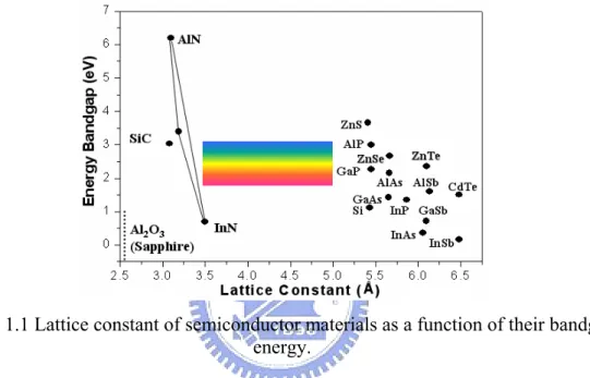
In the history of III-nitride materials, GaN binary alloy was first synthesized by Juza and Hahn with passing ammonia over hot gallium, and produced small needles and platelets for the purpose of studying its crystal structure and lattice constant. In 1958, small crystals of GaN were produced with the same technique by Grimmeiss and Koelmans to measure their photoluminescence (PL) spectra. Ten years later, a large layer of GaN grown on sapphire (Al2O3) substrate by using chemical vapor deposition
technique was demonstrated by Maruska and Tietjen [16]. As regarding the fabrication of GaN-based LED devices, the first demonstration was reported by Pankove et al. in 1971. However, the early works were eventually forsaken because of the lack of advanced epitaxial technique and especially encountering the fundamental material problems. As shown in Figure 1.1, the lattice constant of GaN is 3.189 Ǻ with an energy bandgap of 3.39 eV. At present, sapphire has become the most commonly used substrate for the growth of III-nitride materials. This substrate has several advantages such as cheaper than SiC, high hardness, high heat-resistance, and particularly the free of absorption for green, blue, and ultraviolet photons. However, despite these advantages, there are still some disadvantages; e.g., the interface between GaN and sapphire substrate exists a large lattice mismatch of 15% [8], [9], resulting in a very high dislocation density. Besides, sapphire is a dielectric material, so that both n and p contacts shall be on top of the devices, and etching techniques are inevitably required. Even the sapphire can be the substrate for growing III-nitride materials, the noticeable lattice mismatch, which results in the poor crystal quality, obstructs the early development of III-nitride LEDs.
This high dislocation problem was not solved until 1983 when Dr. Yoshida improved the crystal quality of GaN films with the use of AlN-coated sapphire substrate
[11]. Later, high-quality optically flat surfaces of GaN thin films had been successfully grown by using AlN nucleation buffer layer with metal-organic chemical vapor deposition (MOCVD) technique by Prof. Akasaki et al. [12]. In 1991, S. Nakamura changed AlN thin films with low-temperature growing amorphous GaN thin films as nucleation layer, and mirror-flat GaN thin films were obtained under high-temperature growing [13].
Figure 1.1 Lattice constant of semiconductor materials as a function of their bandgap energy.
Nevertheless, the high n-type background doping in intrinsic GaN film also causes another incapability in fabricating GaN p-n junction LEDs. As many conformation of semiconductor devices, a p-n junction is always required. For n-type GaN, it could be easily achieved with an n-doping level of 1×10¹⁷ ~ 2×1019 cm-3 by Si or Se dopant atoms. For forming p-type GaN layer, even various types of acceptor atoms including Mg and C were tried, it only led to compensated high resistivity material. This bottleneck was first broken through by Akasaki et al. [14] by low energy electron beam irradiation (LEEBI) treatment. A hole concentration of 1×10¹⁷ and a low resistivity of 12 Ω·cm were obtained, respectively. Three years later, the Mg-doped GaN with p-doping level of 3×1018 cm-3 and a resistivity of 0.2 Ω·cm was found more conductive by Nakamura with a treatment of thermal annealing in a N2 ambient [15].
To achieve high-brightness GaN-based LED, another breakthrough of high-quality InGaN films came. In 1990s, a blue InGaN/GaN double-heterostructure LED was fabricated by Nakamura et al. for the first time. With the use of two-flow MOCVD technique, the substrate was heated to 1050 ºC in a stream of hydrogen. Then the temperature was lowered down to 510 ºC for the growth of GaN nucleation layer. Next, the substrate was reheated to 1020 ºC to grow 4-µm n-type GaN film, followed by the 20-nm-thick Si-doped InGaN active layer when the temperature was decreased to 800 ºC. The temperature was then increased to 1020 ºC to grow p-type Mg-doped GaN film. The total thickness was about 4.8 µm, and the surface of p-type GaN was partially etched until the n-type layer was exposed. Finally, a Ni–Au contact was evaporated onto the p-type GaN layer and a Ti–Al contact onto the n-type GaN layer. The peak wavelength was 440 nm with a full width at half maximum (FWHM) of 20 nm at forward current of 20 mA [16].
The first candela-class blue LEDs were fabricated with the use of Si and Zn codoped InGaN active layer. A relatively low indium composition in InGaN layer was used as a result of high-indium InGaN layer might cause the degradation of luminescence intensity. The thickness of InGaN active layer was 50 nm, and the active layer was sandwiched between two 150-nm-thick Al0.15Ga0.85N cladding layers. The
output power and external quantum efficiency at 20 mA were 1.5 mW and 2.7% [17]. Soon afterward, the InGaN/InGaN multiple-QW structures and several novel designs were employed in GaN-based LEDs, and the first commercial GaN-based LEDs were commercialized by Nichia Chemical Company in 1990s. To date, it is less than fifteen years that high-brightness GaN-based LEDs are used throughout the world, for example, in the applications of full-color displays, traffic signals, and other promising areas of high-definition DVD optical storage, chemical processes, and medical applications [18–20].
III-nitride and their alloys represent a very special class of material. They are indeed the best chosen for short wavelength emission due to their wide and direct energy bandgap. Unlike the arsine or phosphide materials, there is not a suitable substrate for their growth, and they are in the hexagonal (wurtzite) crystal system. Mostly, the polarization effect in GaN-based materials has been found much stronger than other III-V compounds [21]. Next, the material properties of wurtzite GaN and its relevant alloys are investigated.
1-1-1 Wurtzite GaN material property
Most III-V compound semiconductor materials are belonged to zinc-blende-type crystals. For GaN and its relevant alloys, they can be zinc-blende type; however, they are commonly grown as wurtzite crystal, which exhibits a hexagonal Bravais lattice, as depicted in Figure 1.2. In crystallography, the wurtzite structure is closely related to the zinc-blende structure, and in fact it is a member of hexagonal crystal system. For most epitaxial GaN growth film, the optic axis (c-axis) [0001] is typically oriented normal to the surface. The strain tensor components are evaluated by specifying five distinct, nonvanished elastic constants for wurtzite crystals:C11, C12, C13, C33, and C44. The
nondiagonal strain-tensor components vanish while ,
lc lc GaN yy xx a a a − = =ε ε . 2 33 13 xx lc lc sub zz C C c c c ε ε = − =−
For the band structure of wurtzite GaN based materials, it is often characterized by the zone-center k⋅ method. The spin-degenerate conduction band is described by the p anisotropic, parabolic form with wave functions comprised of the s-orbital (angular momentum l=0) states: ) ( 2 2 * 1 2 2 2 * // 2 // 2 yy xx zz z c c a a m k m k E H = + + + ε + ε +ε ⊥ h h (1.1)
in which k , k are the wave vectors and m*, * ⊥
the in-plane and c-axis directions. a1 and a2 are the conduction band deformation
potentials. The valence band is described by a 6×6 Hamiltonian transfer matrix including heavy-hole (HH), light-hole (LH), and crystal-field split-off hole (CH) bands [22–24] as follows: ⎥ ⎦ ⎤ ⎢ ⎣ ⎡ = × L U H H H 0 0 6 6 (1.2) where ⎥ ⎥ ⎥ ⎦ ⎤ ⎢ ⎢ ⎢ ⎣ ⎡ + ∆ − ∆ − = λ t t t t t t U iH iH iH G K iH K F H , ⎥ ⎥ ⎥ ⎦ ⎤ ⎢ ⎢ ⎢ ⎣ ⎡ − ∆ − + ∆ = λ t t t t t t L iH iH iH G K iH K F H (1.3)
The matrix elements are
2 2 2 3 6 0 2 2 5 0 2 4 3 2 4 2 3 0 2 2 1 2 2 2 1 0 2 2 1 2 1 2 2 2 ) ( ) ( 2 ) ( ) ( 2 y x t t z t t t yy xx zz t z yy xx zz t z k k k k k A m H k A m K D D k A k A m D D k A k A m G F + = ∆ = ∆ = = + + = + + = + + = + + = + + ∆ − ∆ = + + ∆ + ∆ = h h h h ε ε ε θ θ θ ε ε ε λ λ λ θ λ θ λ ε ε ε ε (1.4)
The Ai parameters are related to the hole effective masses. The crystal field splitting
1
∆ =
∆cr , and the spin-orbit splitting is ∆so =3∆21 =3∆3. As shown in Figure 1.3, the
band structure of wurtzite GaN near the top of valence band is schematically plotted. The bottom two pair bands are the CH splitting bands. The top four bands are split by the spin-orbit interaction into two pairs with heavy and light hole effective masses in the
plane.
Figure 1.2 (a) Wurtzite crystal with lattice constants c and a. (b) The unit cell of wurtzite GaN crystal.
Figure 1.3 Valence-band structure of wurtzite GaN.
1-1-2 Band parameters
Binary alloy
Unlike III-V arsenide and phosphide semiconductor materials, the physics related to GaN based materials has not been well developed. The troubled growth technique and the potentials in GaN based materials are both very attractive that much effort is paid for realizing its material properties. For optoelectronic semiconductor devices, the
bandgap energy of each semiconductor material is undoubtedly one of the most important parameters. As expressed by the Varshni formula [25], the bandgap energy of III-V semiconductor material at temperature T can be:
β α + ⋅ − = T T E T g 2 g( ) (0) E (1.5)
where Eg(T) is the bandgap energy at temperature T, Eg(0) is the bandgap energy
at 0 K, α and β are material-related constants. The value of β is approximately equal to the Debye temperature at 0 K. Several kinds of measurements such as optical absorption, photoreflectance, photoluminescence are employed to determine these constants. In the GaN based materials, binary GaN, AlN, and InN can also be expressed by the Varshni formula accurately within a few meV.
Since the early 1970s, a bandgap energy of 3.5 eV for wurtzite GaN has been realized [26], [27]. To determine the bandgap energy more accurately, a luminescence measurement of the exciton lines is preferred. The research has shown that the actual gap is recovered by adding the estimated binding energy to the observed exciton transition energy. The free A exciton (EA) transition energy, which can be determined
quite precisely, is the most reliable indicator in relatively-pure GaN. A range of A-exciton transition energies at 0 K, 3.474–3.496 eV, has been indicated [28–30], while with A-exciton binding energies range from 18 to 28 meV [31–34]. These values have been critically reviewed by I. Vurgaftman [35], and a value of 3.510 eV for the zero-temperature energy gap is recommended. In the mean time, An average values of the Varshni parameters α =0.909 meV/K and β=830 K are given, while they believe that GaN device characteristics tend to be relatively insensitive to the precise values of the Varshni parameters owing to the small relative change in the energy bandgap (72 meV between 0 and 300 K).
bandgap. As well being a direct-bandgap material the AlN alloy tends to be technologically significant because of its high bandgap property in playing a role of the barrier or cladding layers in the GaN-based devices. The Varshni parameters for AlN, summarized by I. Vurgaftman, obtained with variant measurements such as cathodoluminescence (CL), spectroscopic ellipsometry, and photoreflectance have been obtained. The room temperature energy bandgap of AlN can be in a range of 6.11–6.2 eV. The Varshni parameters α =1.799 meV/K, β=1462 meV for wurtzite AlN are recommended.
As regards wurtzite InN, its bandgap energy determined by optical absorption was early determined to be in a range of 1.7–2.2 eV [36–40]. In stead of using an advanced growth technique to obtain high crystal quality, the thin InN film was sputtered, which in term results in an uncertainty. Before 2001, most has believed that the energy bandgaps of wurtzite InN at low temperature and room temperature are 1.997 and 1.97 eV, respectively. The Varshni parameters are α =0.245 meV/K, β=624 meV [41]. This InN energy bandgap value is repudiated in 2001 since single crystal InN film is successfully obtained. The re-evaluated wurtzite InN bandgap energy is in the 0.7–0.8 eV range [42], [43]. The Varshni parameters are regarded unchanged as prior. Other significant band parameters such as effective masses, splitting energies, and deformation potentials etc. for GaN, AlN, and InN binary alloys are listed in Table 1.1 [35].
Table 1.1 Band parameters of wurtzite binary GaN, AlN, and InN alloys. Parameters GaN AlN InN
lc a (Ǻ) at T=300 K 3.189 3.112 3.545 lc c (Ǻ) at T=300 K 5.185 4.982 5.703 g E (eV) 3.51 6.25 0.78 α (meV/K) 0.909 1.799 0.245 β(K) 830 1462 624 cr ∆ (eV) 0.010 -0.169 0.040
so ∆ (eV) 0.017 0.019 0.005 // e m 0.2 0.32 0.07 ⊥ e m 0.2 0.30 0.07 1 A -7.21 -3.86 -8.21 2 A -0.44 -0.25 -0.68 3 A 6.68 3.58 7.57 4 A -3.46 -1.32 -5.23 5 A -3.40 -1.47 -5.11 6 A -4.9 -1.64 -5.96 7 A (eV Ǻ) 0.0937 0 0 1 a (eV) -4.9 -3.4 -3.5 2 a (eV) -11.3 -11.8 -3.5 1 D (eV) -3.7 -17.1 -3.7 2 D (eV) 4.5 7.9 4.5 3 D (eV) 8.2 8.8 8.2 4 D (eV) -4.1 -3.9 -4.1 5 D (eV) -4.0 -3.4 -4.0 6 D (eV) -5.5 -3.4 -5.5 11 c (GPa) 390 396 223 12 c (GPa) 145 137 115 13 c (GPa) 106 108 92 33 c (GPa) 398 373 224 44 c (GPa) 105 116 48 13 d (pm/V) -1.6 -2.1 -3.5 33 d (pm/V) 3.1 5.4 7.6 15 d (pm/V) 3.1 3.6 5.5
Ternary InGaN and AlGaN alloys
For nitride based ternary alloys, due to the smaller bandgap energy of InGaN material than that of GaN, InGaN ternary alloy can be used as a promising active heterostructrue or QW material to emit in the violet and blue region of the spectrum with a carrier confinement layer of AlGaN. The In and Al content in each respective layer is commonly less than 20% when consider having a high quality film. In 1990, there has been significant process in the growth and characterization of the InGaN material [44–46]. The bandgap energy of InGaN measured by Osamura et al. [47]
across the entire compositional range has a smooth variation with some bowing by ) 1 ( ) ( ) 1 ( ) ( )
(InGaN v E InN v E GaN b v v
Egv = ⋅ g + − ⋅ g − InGaN⋅ ⋅ − (1.6)
. The bandgap energy of the ternary alloy is assumed with linear combination of two binary alloys with a second-order correction. The b value is so-called bowing parameter which is accounted for the deviation from the linear interpolation between the two binary alloys. A bowing parameter value of 1.0 eV for InGaN is early found either by experimentally fit to the PL data or numerical calculations [48–52]. A large bowing value in a range of 2.4–3.5 eV is also proposed, while I. Vurgaftman recommends that a bowing parameter value of 1.4 eV for InGaN [35], which bases on several prior works and the consideration of recent growth of high-quality high In content epitaxial film.
For AlGaN ternary alloys, Yoshida et al. observed that the band gap energy of AlGaN deviates upwards with increase in AlN composition [53]. Hagen et al. and Koide et al. observed that the bandgap energy of AlGaN deviated downward with the increase of AlN composition [54], [55]. They all believed that the bandgap energy could be described with linear combination of AlN and GaN binary alloys with a second-order correction by ) 1 ( ) ( ) 1 ( ) ( )
(AlGaN w E AlN w E GaN b w w
Egw = ⋅ g + − ⋅ g − AlGaN⋅ ⋅ − (1.7)
Even a large number of bowing parameter values is proposed, most researchers believes that the bowing parameter for AlGaN is positive, corresponding to be in a range of 0.353–1.38 eV [56–60]. A bowing parameter value of 0.7 eV for AlGaN, based on the consistent finding of the relatively small bowing parameter by the theories and experiments, is recommended by I. Vurgaftman [35].
Despite of the bandgap energy of ternary alloy can be expressed in linear combination of binary alloys with a bowing, other band parameters such as effective masses, splitting energies, and deformation potentials etc. for ternary alloy can be
calculated from the linear interpolation between the two binary alloys but with zero bowing parameter.
Quaternary InGaAlN alloy
While considering an optoelectronic light emitting device emitting in ultraviolet wavelength region, quaternary InGaAlN is preferred to be the active region material due to the lattice constant of InGaAlN can be tuned match, either tensile or compressive to GaN. That the design in QW active region can be more optimized therefore obtaining better output characteristics. Prior studies have found that the lattice mismatch is reduced by the incorporation of In with an In/Al ratio close to 1/5 and match to GaN [61]. Mostly, the band parameters of quaternary alloys can be expressed in linear interpolation formula as ) ( ) ( ) 1 ( ) ( )
(In Ga1 Al N x P InN x y P GaN y P AlN
P x −x−y y = ⋅ + − − ⋅ + ⋅ (1.8)
For the energy bandgap of InGaAlN, some has reported with rather small In fraction. M Asif Khan found that the energy bandgap of InGaAlN reduced almost linearly when In <2% [61]. A relationship for the calculation of composition dependent parameters by a weighted sum of ternary alloys has also been permitted, for instance, the bandgap energy of InGaAlN can be [62]
zx yz xy AlGaN E zx InGaN E yz AlInN E xy InGaAlN Eg gu gv gw + + ⋅ + ⋅ + ⋅ = ( ) ( ) ( ) ) ( (1.9) with ) 1 ( ) ( ) 1 ( ) ( )
(AlInN u E InN u E AlN b u u
Egu = ⋅ g + − ⋅ g − AlInN ⋅ ⋅ − (1.10) 2 1 2 1 2 1 x z w z y v y x u= − + = − + = − + (1.11)
where x, y , and z=1−x−y represent the compositions of Al, In, and Ga in the InGaAlN alloy. The bandgap energy of ternary InGaN and AlGaN are depicted in expressions (1.6) and (1.7).
1-1-3 Spontaneous and piezoelectric polarizations
Built-in electric fields in semiconductors can be caused by spontaneous polarization P and by strain-induced polarizationsp Ppiezo . In c-face nitride-based
materials, these polarization effects were found much stronger when compared to other semiconductor materials [21]. In this situation, electrons and holes are separated in the quantum well, as indicated in Figure 1.4, the transition energy is reduced by the built-in field, leading to a red-shift of the emission wavelength. The wider the quantum well thickness, the more separated electrons and holes, and the less overlap of electron and hole carrier density distributions, which leads to a smaller optical gain and less spontaneous emission.
Figure 1.4 Band edges of conduction and valence bands
Fiorentini et al. has developed a way to estimate the interface charge density [63]. The spontaneous polarization of ternary nitride alloys can be expressed by
) 1 ( 071 . 0 ) 1 ( 042 . 0 090 . 0 ) ( ) 1 ( 038 . 0 ) 1 ( 034 . 0 042 . 0 ) ( ) 1 ( 019 . 0 ) 1 ( 034 . 0 09 . 0 ) ( 1 1 1 x x x x N In Al P x x x x N Ga In P x x x x N Ga Al P x x sp x x sp x x sp − ⋅ ⋅ + − ⋅ − ⋅ − = − ⋅ ⋅ + − ⋅ − ⋅ − = − ⋅ ⋅ + − ⋅ − ⋅ − = − − − (1.12)
As yet, there is no investigation on polarization properties focusing on the quaternary InGaAlN alloy. Only a similar way to that shown in expression 1.9 can be used for the calculation. The piezo-electric polarization can be calculated by
2 2 2 2 559 . 7 373 . 1 ) ( 541 . 9 918 . 0 ) ( 0 888 . 7 808 . 1 ) ( 0 624 . 5 808 . 1 ) ( ε ε ε ε ε ε ε ε ε ε ⋅ + ⋅ − = ⋅ + ⋅ − = > ⋅ − ⋅ − = < ⋅ + ⋅ − = InN P GaN P for AlN P for AlN P pz pz pz pz (1.13)
where ε is the basal strain of the binary compound considered. Linear interpolation formula is used for the calculation of ternary and quaternary nitride alloys. The total built-in polarization is the sum of spontaneous and piezo-electric polarizations.
1-1-4 Band alignment discontinuity
The value of band-offset is quite significant for the design of heterostructure devices. This value also plays a very important role in the analysis of energy band diagram. It is obvious that when two different materials are grown next to each other, both the conduction and the valence bands of the two materials will possess discontinuities at the interface. Quality and even feasibility of heterojunction device concepts often depend crucially on values of these band offsets. Several researchers determined the band-offset values of II-VI and III-V heterostructures experimentally by growth techniques such as MBE and MOCVD. Theoretical calculation indicated that the electronic structure in each layer of a heterojunction became nearly bulklike even a single atomic layer away from the interface, lending credence to the idealized notion of an abrupt band edge discontinuity. To determine band-offset values of semiconductor materials, X-ray photoelectron spectroscopy (XPS) and ultraviolet photoelectron spectroscopy (UPS) are primarily used by means of electron core level energies. Optical techniques, such as excitation PL and reflectivity, also present a more accurate tool to determine band-offset values. However, the devotion of the determination of the band-offset values in semiconductor heterojunction from experimental measurements and theoretical calculations exist large discrepancies, which may be related to the
difficulty of obtaining high quality epitaxial films.
Various types of band alignments can arise in semiconductor interfaces depending on the relative adjustment of energy bands with respect to each other. For semiconductor heterojunctions, there are two most common types of alignments. Type I alignment shows that the bandgap of one semiconductor lies completely within the bandgap of the other. This type is the most useful one for optoelectronic devices because the carriers are well confined in the smaller bandgap region. Type II alignment is the bandgaps of two materials overlap but not completely covering the other. For nitride-based materials, they all belongs to type I, and six different kinds of heterojunction combination, such as AlN/GaN, InN/GaN, GaN/AlN, InN/AlN, AlN/InN, and GaN/InN (A/B represents that A thin film is grown on top of B material) list. Table 1.2 lists some band-offset values of wurtzite nitride binary alloys reported by Martin et al. InN/GaN–GaN/InN and InN/AlN–AlN/InN heterojunctions show a significant forward-backward asymmetry. AlN/GaN–GaN/AlN heterojunctions give almost identical values. The asymmetric nature may be provided by strain induced piezoelectric fields [64] due to that the lattice constant of InN alloy is much larger than those of AlN and GaN, and the lattice mismatch between AlN and GaN is relative smaller than that between GaN and InN.
Table 1.2 Valence band-offset values of wurtzite nitride binary alloys (Unit: eV). Reference AlN/GaN InN/GaN GaN/AlN InN/AlN AlN/InN GaN/InN
[65] 0.8±0.3 ~ 0.8±0.3 ~ ~ ~ [66] 0.57±0.22 0.93±0.25 0.60±0.24 1.71±0.20 1.32±0.14 0.59±0.24 [67] ~ ~ 0.5±0.5 ~ ~ ~ [68] 1.36±0.07 ~ ~ ~ ~ ~ [69] 0.81 0.48 0.81 1.25 1.25 0.48 [70] 0.84 0.26 0.84 1.04 1.04 0.26
1-2 Historical review of RCLEDs
Novel concept of RCLED is first proposed and demonstrated by Schubert et al. in 1992 [71]. The active region of the device is placed in a resonant optical cavity, and the cavity is defined by a highly reflective (99%) and a moderately reflective mirror. As shown in Figure 1.5, the optical cavity mode can be in resonance with spontaneous emission of the active region. As a typical design of the optical cavity, it often has a thickness of 1/2- or 1-λ of the light emitted by the active region. The optical mode density can be strongly enhanced for on-resonance wavelengths. As a consequence, on-resonance transitions of the RCLEDs are enhanced. With the help of bottom highly reflective mirror, emission of light through the top side is enhanced, typically by a factor of two.
Figure 1.5 A schematic layer consequence of the RCLED device.
The placement of an active region inside a resonant cavity results in several improvements of the device characteristics. In comparison to typical LEDs, RCLEDs enjoy improved spectral purity, highly directional light output, less chromatic dispersion and improved modulation bandwidth. The spectral emission linewidth of a typical LED is determined by the thermal energy kT. However, the emission linewidth in RCLED is
DBRs High reflector Moderate reflector Optical cavity DBRs 1 λ
determined by the quality factor (Q factor), which is defined as 2 1 2 1 4 2 1 1 2 1 2 R R L n R R R R L n Q c cavity c cavity − ⋅ ⋅ ≈ − ⋅ ⋅ = ∆ = π λ π λ ν ν (1.14)
where Lc is the cavity length, ∆ν and ν are the linewidth and frequency of the
Febry-Pérot resonance mode. R is the respective top and bottom reflectivity. As a result, the spectral linewidth of the RCLED can be a factor of 2–5 narrower to typical LED. Moreover, the emission wavelength shit with temperature is determined by the temperature coefficient (dλcavity/dT) of the optical cavity, not by the energy gap of the active region. This results in a higher temperature stability of the RCLED emission wavelength compared with typical LEDs. As compared with vertical-cavity lasers, the epitaxial complexity of RCLED structure is reduced since the reflectivity of upper distributed Bragg reflectors (DBRs) has to be less than 90%, and thus the RCLEDs provide thresholdless operation and better fabrication reliability.
1-2-1 RCLED design rules
A fundamental structure of an RCLED is plotted in Figure 1.6. Two mirrors with reflectivity R1 and R2 comprise a cavity and the active region is embedded. The
reflectivity of the two mirrors is chose to be unequal so that the light exits the cavity predominantly through one of the mirrors. The active region shall be located preferably at the antinode location of the optical standing wave of the cavity. The active region has a thickness of Lactive and an absorption coefficient of α . The cavity shows a
one-wavelength cavity with a length of Lcavity. Owing to the light extraction, a
fundamental design criterion for RCLED is that the light-exit reflector, R1, should be
emit in one direction. This is important for the light coupling into the small-core fiber, and in the application of display RCLED, where light should be emitted towards the observer. R1 Active R2 region Lactive Lcavity R1 Active R2 region Lactive Lcavity
Figure 1.6 Schematic illustration of a resonant cavity consisting of two mirrors with reflectivity R1 and R2.
Secondly, the criterion arises from the design of the cavity length, Lcavity, which
shall be as shorter as possible. As an expression of the integrated enhancement ratio, also called suppression ratio, given by
π σ λ π 2 1 2 int = ⋅Ge⋅∆ ⋅ G (1.15)
where it is assumed that the emission spectrum is in Gaussian distribution with a peak value of (σ(2π)1/2)−1 and a linewidth of ∆λ =2σ(2ln2)1/2
n . Ge is an enhancement
factor at the resonance wavelength given by the ratio of the optical mode densities with and without a cavity as
0 2 2 1 1 4 / 1 2 1 ) 1 ( ) 1 ( ) ( 2 2 density mode optical minimal density mode optical maximal τ τ π π ξ cavity e R R R R R G ⋅ − − ⋅ ⋅ = = (1.16)
where the enhancement factor ξ has a value of 2 if the active region is located exactly at an antinode of the standing wave inside the cavity, and equals to 1 if the active region is smeared out over many periods of the standing wave. When the active region is located at a node, ξ =0. τcavity and τ0 represent the spontaneous emission lifetime
cavity lifetime is reduced as a result of the cavity. ∆λ is the cavity resonance bandwidth.
Finally, the integrated enhancement ratio can be
0 2 1 1 int ln2 1 1 2 2 τ τ λ λ λ π π ξ cavity cavity cavity n L R R R G ⋅ ⋅ ∆ ⋅ ⋅ − − ⋅ ⋅ = (1.17)
where λ and λcavity are the active region emission wavelength in vacuum and inside
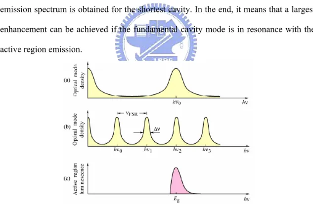
the cavity. One can easily observe that the light intensity can be enhanced by the minimization of the cavity length. The importance of a short cavity length is elucidated in Figure 1.7. The respective optical mode densities of two different cavities are shown in Figure 1.7(a) and (b). The natural emission spectrum of the active region is shown in Figure 1.7(c). A good overlap between the resonant optical mode and the active region emission spectrum is obtained for the shortest cavity. In the end, it means that a largest enhancement can be achieved if the fundamental cavity mode is in resonance with the active region emission.
Figure 1.7 Optical mode density for (a) a short and (b) a long cavity. (c) Spontaneous emission spectrum of an LED active region.
While the emission from the active region resonates in the cavity, the phenomenon of self-absorption in the active region comes. It is in criterion that the re-absorption probability of photons emitted from the active region into the cavity mode shall be
much smaller than the extraction probability of photons, which can be written as
) 1
(
2⋅ξ⋅α⋅Lactive < −R1R2 (1.18)
As an example of 650-nm RCLED with InGaP/InGaAlP active region, the reflectivity of two mirrors are design as R1~70% and R2 ~100%, and the active region is
assumed to be located well in the antinode of the optical standing wave with ξ =2. The absorption coefficient for InGaP at 650 nm is assumed 10000 cm-1. This criterion can be fulfilled if the active region thickness is less than 75 nm. That means the period of QWs in the active region is limited. If the criterion of expression 1.17 can not be fulfilled, photons will be re-absorbed by the active region, which in turn results in the re-emission along the lateral direction, not into the cavity mode or a possibility of non-radiation from the generated electron-hole pairs [72].
1-2-2 RCLED applications
The characteristics of RCLED shown above are desirable for local-area medium bit rate optical communication systems. In short-distance communication systems, polymethyl methacrylate plastic optical fibers (POFs) are increasing used as it provides a relatively low cost. Figure 1.8 shows the attenuation loss as a function of the wavelength in PMMA core fiber. At 650 nm, the preferred communication wavelength for POFs exists a relatively minimal attenuation loss of 0.15 dB/m [73]. Recently, the application of POFs has been extended to the automotive industry, such as media oriented systems transport (MOST), which needs to carrier 50–250 Mbps of data over POFs. MOST is a networking standard intended for interconnecting multimedia components in automobiles and other vehicles. It differs from existing vehicle bus technologies in that it's intended to be carried largely on an optical fiber bearer, thus providing a bus-based networking system at bit-rates far higher than available on
previous vehicle-bus technologies. MOST technology provides an environment where hardware is no longer the limiting factor to new multimedia application development. By approaching the network from a full system standpoint, all layers required for application development and system management have been defined and standardized.
Figure 1.8 Attenuation of a PMMA step-index POF.
Figure 1.9 MOST technique concepts in home and automotive multimedia networking. As depicted in Figure 1.9, entertainment functions can be distributed around the system with MOST. For example, a DVD player sends audio and video around the network for playback at several locations simultaneously. Intelligent but very low cost