國 立 交 通 大 學
電子物理研究所碩士班
碩 士 論 文
一種具有奈米線通道的新穎多晶矽薄膜電晶體
製作與特性之研究
Fabrication and Characterization of a Novel
Polycrystalline Silicon Thin Film Transistor with
Nanowire Channels
研 究 生:林賢達
指導教授:趙天生 博士
一種具有奈米線通道的新穎多晶矽薄膜電晶體
製作與特性之研究
Fabrication and Characterization of a Novel Polycrystalline
Silicon Thin Film Transistor with Nanowire Channels
研 究 生:林賢達 Student:Hsien-Ta Lin
指導教授:趙天生 博士 Adviser:Tien-Sheng Chao
國 立 交 通 大 學
電子物理研究所碩士班
碩 士 論 文
A Thesis
Submitted to Institute and Department of Electrophysics
National Chiao Tung University
in partial Fulfillment of the Requirements
for the Degree of
Master
in
Electrophysics
June 2005
Hsinchu, Taiwan, Republic of China
中華民國九十四年六月
一種具有奈米線通道的新穎多晶矽薄膜電晶體
製作與特性之研究
研究生:林賢達 指導教授:趙天生 博士
國立交通大學 電子物理研究所碩士班
摘 要
在本篇論文中,我們製作了一種具有奈米線通道的新穎多晶矽薄膜電
晶體,並測量了它的特性。一般來說,製作奈米線結構需要昂貴的設備或
運用複雜的過程。我們提出一種簡單快速製備奈米線之方法。利用一般製
作氧化層邊襯(oxide spacer)之方法概念,以底閘極薄膜電晶體結構來形
成多晶矽邊襯奈米線通道(poly-Si sidewall spacer nano-wire channel)。可藉
由調整閘極高度、非晶矽沉積厚度和蝕刻時間,來控制此邊襯之直徑至 30nm
以下。此製作程序與傳統製程設備相容,且不需要其它困難的技術。元件
完成總共只需要四道光罩,是低成本的製程。
在研究中,我們測量了不同條件的奈米線通道之元件特性。為了更進
一歩改善元件特性,我們對元件分別做了
N
2/H
2退火及
NH
3電漿處理。我
們發現
NH
3電漿處理比
N
2/H
2退火能更有效改善元件特性,例如:鈍化缺
陷、降低漏電流、提升載子遷移率、增強開啟電流等。NH
3電漿處理對於
元件輸出特性也有所改善,在高汲極偏壓下能有效抑制
kink effect。在文
中,我們也分析並討論了有關漏電流的造成因素,並提出了兩個造成漏電
流的機制和其他影響漏電流的可能原因。
在未來,為了改善原件特性,有效減少多晶矽薄膜的缺陷是很重要的。
而使用金屬誘發側向結晶法和準分子雷射結晶法,可以達到增大多晶矽結
晶的目的,相信可以大大提升元件特性。只要元件特性夠好,此元件技術
可以應用在各種先進應用方面。
Fabrication and Characterization of a Novel Polycrystalline Silicon
Thin Film Transistor with Nanowire Channels
Student: Hsien-Ta Lin Adviser: Dr. Tien-Sheng Chao
Institute and Department of Electrophysics
National Chiao-Tung University
Abstract
In this thesis, we fabricated a novel poly-Si TFT with nanowire channels and measured its characteristics. Generally, the traditional method is expensive and complicated to obtain the nano-wire structure. We proposed a simple and fast approach to manufacture the nano-wire. Using the method of forming oxide spacer, we form the poly-Si sidewall spacer nano-wire channels for the bottom-gate TFT. Thus, we can control the sidewall spacer nano-wire thickness under 30 nm by controlling the gate height, α-Si layer thickness, and etching time. The process is compatible to conventional process equipment, and doesn’t need any difficult technique. The total mask number to complete the device is only four, so it is a low-cost process.
In this study, we characterized the performance of poly-Si NW TFTs for various nano-wire conditions. In order to improve the device performance, we executed the N2/H2 gas
annealing and NH3 plasma treatment. However, the NH3 plasma treatment can improve the
device performance more effectively than N2/H2 gas annealing, such as passivate the defects,
subthreshold slope. The NH3 plasma treatment also can improve the device output property, and suppress the kink effect at high drain bias effectively. We also analyzed and discussed the origins of the off-state current, and proposed two mechanisms to explain the origins of leakage current and the other probable reasons for our device.
In the future, to further improve the device performance, it is important to reduce the defects and trap-states in poly-Si film for the poly-Si NW TFT. This could be achieved by using the metal induce lateral crystallization (MILC) or excimer laser crystallization (ELC) to enlarge the grain size of the poly-Si films. We believe that can greatly improve the device performance. As long as the performance reaches good enough, it can be applied to a variety of novel applications in the future.
誌
謝
首先我要感謝的是指導教授 趙天生博士、 林鴻志博士與 黃調元博
士,在碩士班兩年的時間裡給我研究的方向並讓我了解如何做研究,如何
去分析問題,並且感謝他們無論在生活上、學業上給我的關心、鼓勵與鞭
策。接著特別感謝實驗室帶我的李明賢學長、蘇俊榮學長,從實驗儀器的
操作、元件製作到材料分析及元件電性量測都給我莫大的幫助。而呂嘉裕
學長、盧文泰學長、李耀仁學長、葉冠麟學長在實驗製作與量測分析上也
給我許多指導與建議。也感謝實驗室的各個同學張伊鋒、藍文廷、李聰杰、
房新原、于慶潭、王仁杰、吳浩偉及學弟妹們、專題生,在研究所的生活
中一起努力、相互勉勵。還有國家奈米元件實驗室(NDL)的工程師沈士文
學長,感謝他耐心地幫忙準備 TEM 試片及 TEM 拍照的工作。以及國家奈米
元件實驗室的其他工程師和員工,感謝他們辛苦維護機台,提供了完善的
環境、設備及技術支援給我,讓元件製程能順利的完成。另外也感謝我的
室友及電子所、電物所、材料所、管科所的好朋友,陪我度過充實的研究
所時光。最後要感謝我的父母,無論在生活上、經濟上都給我很大的幫助,
讓我能夠無憂無慮地專心攻讀研究所,在精神上也給我無比的支持與鼓
勵。在此再次感謝以上的所有人無論是生活上或是學業上給我的幫助,讓
我順利完成研究所學業
。Contents
Abstract (in Chinese)………..………I Abstract (in English)………..…………... III Acknowledgement (in Chinese)………..………. V Contents………VI Table Captions……….VII Figure Captions………..VIII
Chapter 1 Introduction... 1
1-1 Background and motivation ...1
1-1-1 Overview of polycrystalline silicon thin film transistors...1
1-1-2 Overview of nanowire...4
1-2 Thesis organization ...7
Chapter 2 Device Fabrication and Operation Principles ... 8
2-1 Device structure and fabrication ...8
2-1-1 Experimental procedures ...8
2-1-2 Experimental results ... 11
2-2 Operation of poly-Si NW TFT ...12
Chapter 3 Characteristics and Discussion of NW TFT ... 14
3-1 Device performance ...14
3-2 Effects of post treatment ...17
3-3 Origins of leakage current...19
Chapter 4 Conclusions and Future Works ... 25
4-1 Conclusions ...25
4-2 Future works...26
Table Captions
Table 2-1 Etching recipe of the high-density plasma and the corresponding etching
selectivity of poly-Si to SiO2...32
Table 2-2 NH3 plasma treatment conditions. ...32
Table 2-3 Split conditions ...33
Table 2-4 Summary of the features size of nano-wire with 100nm gate by TEM...34
Table 3-1 The summary of characteristic parameters various channel layer thickness and over etching time at VD=0.5V.(SPC before etching)...35
Table 3-2 Comparison of characteristic parameters among as-fabricated FG-annealed, and NH3 plasma-treated n-channel devices,all at VD=0.5V. ...36
Table 3-3 The comparison on n-channel device characteristics between as-fabricated, NH3 plasma treatment 1hr, and 2hrs...36
Table 4-1 Summary of the major features of conventional top-down and bottom-up approaches, and our approach. ...37
Figure Captions
Figure 2-1 (a) Device structure of the proposed poly-Si NW TFT. ...38
Figure 2-1 (b) Top-view layout of the poly-Si NW TFT...38
Figure 2-2 The key process flow of poly-Si NW TFT. ...39
Figure 2-3 Definition of the nanowire width and thickness. ...41
Figure 2-4 (a) Cross-sectional TEM picture of the sample(1). ...42
Figure 2-4(b) SEM picture of the sample(1). ...42
Figure 2-5 Cross-sectional picture of sidewall spacer nano-wire channel of sample(2) by TEM...43
Figure 2-6 Cross-sectional picture of sidewall spacer nano-wire channel of sample(3) by TEM...43
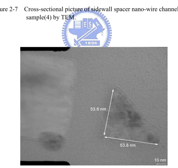
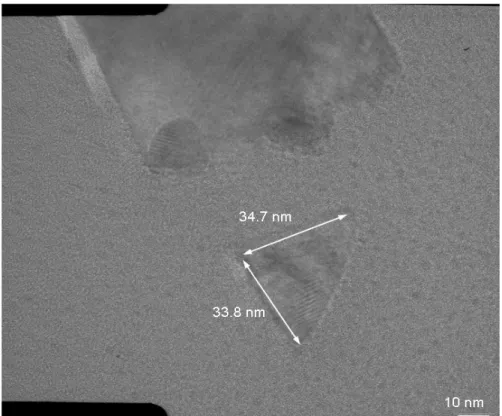
Figure 2-7 Cross-sectional picture of sidewall spacer nano-wire channel of sample(4) by TEM...44
Figure 2-8 Cross-sectional picture of sidewall spacer nano-wire channel of sample(6) by TEM...44
Figure 2-9 Cross-sectional picture of sidewall spacer nano-wire channel of sample(7) by TEM...45
Figure 2-10 Cross-sectional picture of sidewall spacer nano-wire channel of sample(8) by TEM...45
Figure 2-11 Cross-sectional picture of sidewall spacer nano-wire channel of sample(9) by TEM...46
Figure 2-12 Cross-sectional nanowire width and thickness as a function of over etching time by In-line SEM for samples(2), (3), and (4)...46
Figure 3- 2 Typical transfer characteristics of devices with over etching of 30s and over
etching 40s. ...47
Figure 3- 3 Typical transfer characteristics of devices with over etching of 20s and over etching 25s...48
Figure 3- 4 Typical transfer characteristics of devices with nanowire thickness of 54 and 30 nm...48
Figure 3-5 (a) Typical transfer characteristics of devices with channel layer SPC before plasma etching and SPC after plasma etching (OE40s)...49
Figure 3-5(b) Typical transfer characteristics of devices with channel layer SPC before plasma etching and SPC after plasma etching (OE20s)...49
Figure 3- 6 Typical transfer characteristics of n-channel and p-channel devices. ...50
Figure 3- 7 Vth and its deviation as a function of channel length. ...51
Figure 3- 8 On-state drain current versus channel length at VG=10V and VD=0.5V. ...51
Figure 3-9 (a) ID-VD output characteristics of a short channel device (L = 1m)...52
Figure 3-9 (b) ID-VD output characteristics of a long channel device (L = 5 m). ...52
Figure 3-10 (a) ID-VD output characteristics of a short channel device ...53
Figure 3-10 (b) ID-VD output characteristics of a short channel device (L =5 m)...53
Figure 3- 11 Energy band diagram along the channel at VD=0V and VD=high voltage. ...54
Figure 3-12 (a) Cross-sectional view of the saturation region in the intrinsic n-channel poly-Si TFT. ...55
Figure 3-12 (b) Diagram illustrating the current continuity for the impact-ionization mechanism initiated by the DIGBL current in the intrinsic n-channel poly-Si TFT...55
Figure 3- 13 The ID-VD output characteristics of devices with SPC before and after etching.
...56 Figure 3-14 (a) ID-VD output characteristics of a short p-channel device...57
Figure 3-14(b) ID-VD output characteristics of a p-channel device (L = 5 m). ...57
Figure 3-15 Subthreshold characteristics of as-fabricated device and devices with N2/H2 gas
annealing 0.5hr, and NH3 plasma treatment-1hr. ...58
Figure 3-16 Transfer characteristics of as-fabricated device and device with 2-hour NH3
plasma treatment at VD=0.5V. ...59
Figure 3-17 Subthreshold characteristics of as-fabricated device and devices that received 1- and 2-hour NH3 plasma treatment at VD=0.5V. ...59
Figure 3-18 ID-VG characteristics of devices with SPC before and after etching and received
NH3 plasma treatment 1hour. ...60
Figure 3-19 (a) ID-VD output characteristics of as-fabricated device and device with NH3
plasma treatment for 2 hours.(L = 1 m)...61 Figure 3-19 (b) ID-VD output characteristics of as-fabricated device and device with NH3
plasma treatment for 2 hours.(L = 5 m)...61 Figure 3-20 Leakage current as a function of overetch time for samples with SPC before and after channel etching...62 Figure 3-21 (a) ID-VG characteristics of the as-fabricated device with various VD. ...63
Figure 3-21(b) ID-VG characteristics of the device received 2-hour NH3 plasma treatment
with various VD. ...63
Figure 3-22 (a) Off-state leakage characteristics characterized at various temperatures. ...64 Figure 3-22 (b) Arrhenius plots of the off-state current of 0.8µm n-channel device at
different gate voltages. The slope of each line determines the activation energy (Ea)...64
Figure 3-23 (a) Dependency of activation energy on gate and drain voltages for an
as-fabricated device...65
Figure 3-23 (b) Dependency of activation energy on gate and drain voltage for a device received 2 hour NH3 plasma treatment. ...65
Figure 3- 24 The band diagrams for mechanism 1. ...66
Figure 3- 25 The gate-drain overlap region and the definition of gate wdith...67
Figure 3-26 (a) Off-state current with various gate width at VD=5V. ...68
Figure 3-26 (b) Off-state current with various gate width at VG=-5V and VD=5V...68
Figure 3- 27 Dependency of activation energy on gate and drain voltages for a device received 2 hour NH3 plasma treatment. ...69
Chapter 1
Introduction
1-1 Background and motivation
1-1-1 Overview of polycrystalline silicon thin film transistors
Thin film transistors (TFTs), which employ a thin semiconductor film on an insulating substrate as the active device channel, was first demonstrated in 1961 by Dr. P. K. Wenimer in RCA. With its simplicity in structure and fabrication, the applications of thin film transistors in image sensors and displays become more and more popular. Polycrystalline silicon deposited by low-pressure chemical vapor deposition (LPCVD) technique is widely used in modern very large scale integrated (VLSI) circuit [1-3]. The first polycrystalline silicon thin film transistors (poly-Si TFTs) were fabricated by Fa et al [4] in 1966. Since then, electrical properties, conduction mechanism and fabrication process of polysilicon films were widely and extensively studied [5][6].
Active matrix-addressed flat-panel liquid crystal displays (AMLCDs) are one of the most promising candidates for realizing high-quality large-area flat-panel displays [7]. The traditional AMLCDs were fabricated using α-Si:H TFTs for the pixel switching device. Amorphous silicon thin film transistors, among many types of active elements, have been intensively studied because of their many advantages, particularly their compatibility with large glass substrate with low processing temperature [8]. However, the low electron field-effect mobility attainable (<1 cm2V-1s-1 ) with these devices limits their applications for
on the same substrate is very desirable not only to reduce the cost but also to improve the circuit and system reliability. Recently, poly-Si has been proposed as a very attractive alternative material for the active element of LCDs. During the past decade there has been a rapid growth of interest in polycrystalline silicon (poly-Si) for the active device layer in thin film transistors (TFTs) for AMLCDs [9][10][11]. This is due to the much higher mobility and the drive current of poly-Si TFTs, compared to amorphous silicon counterparts, which enables the integration of peripheral circuit on the same panel in active matrix liquid crystal displays [1]. The superior field effect mobility (>100 cm2V-1s-1 ) achieved with poly-Si thin film transistors seems to be essential for the successful integration of row and column drive circuits on the active plate.
The performance of poly-Si TFTs is strongly influenced by grain boundaries and intragranular defects [12]. In order to enhance TFTs characteristics, several techniques used to increase the grain size of poly-Si films have been proposed and developed [13][14][15], such as direct deposition of poly-Si at a reduced pressure (e.g., <10 mTorr), as well as conversion from an amorphous precursor state. The latter approaches include:
1. Solid-Phase Crystallization (SPC):
Although solid-phase crystallization of the amorphous silicon films had been studied by Koster in 1978 in the context of solar cell work, the interest in the technique for TFT work was stimulated by the work of other people. This method is the crystallization of amorphous silicon (α-Si) films deposited by low-pressure chemical vapor deposition (LPCVD) [16]. For α-Si films deposited at temperature below 600 , thermal crystallization for 20 hours at ℃ 600 was required to convert them into their final poly℃ crystalline form. The grain size obtained by solid-phase crystallization (SPC) of α-Si films is larger by several times and has smoother surface morphology than that of as-deposited poly-Si films. Grain size dimensions in excess of 1 µm have been obtained by this technique.
2. Metal-Induced Lateral Crystallization (MILC):
MILC employs metal as precursor to lead amorphous Si to re-crystallize at lower temperatures because of lower energy barrier of re-crystallization resulting from the reaction between metal and Si [17].
3. Excimer Laser Crystallization (ELC):
The conventional approach for producing low-defect-density polysilicon films is the solid-phase crystallization (SPC) of thin amorphous-silicon films on glass substrate by furnace annealing near 600 . Pulsed UV℃ -excimer laser annealing is also being investigated as an alternative crystallization technique to replace furnace annealing [18]. The standard gas mixtures and output wavelengths are ArF(193nm), KrF(248nm) and XeCl(308nm). For fabricating high performance poly-Si TFTs on a glass substrate, excimer laser crystallization method is very promising for the following reasons. First, it is a low-temperature process that introduces no serious thermal shrinkage of the glass substrate caused by the effects of the short pulse and large absorption coefficient of silicon in the UV light regime. Secondly, it can crystallize the film selectively by partially irradiating the film surface, so both poly-Si TFTs and amorphous Si TFTs can be formed on the same substrate. The laser process heats the thin silicon film to melting point on a short time scale (10ns~30ns) the allows the film to melt and recrystallize without significantly heating the glass substrate. Since this process achieves higher annealing temperature than a conventional furnace annealing, significantly higher quality polysilicon film can be obtained.
While there is a high-temperature technology based on the use of quartz substrate, people focus on the film processing at a sufficiently low temperature(<630℃)to permit the use of inexpensive glass substrates.
single-crystal counterparts because of the presence of grain boundaries in the channel. Polycrystalline silicon is rich in grain boundary defects as well as intragrain defects, and the electrical activity of these charge-trapping centers profoundly affects the thin film transistor characteristics. Due to the high density of defect states at grain boundaries and interior of grains, poly-Si TFTs exhibit poor performance such as low mobility, large subthreshold swing, large threshold voltage, and large leakage current, as compared to single-crystal counterparts. The electrical properties of polycrystalline semiconductor devices are strongly affected by the defects such as dangling bonds and strained bonds located at or near the grain boundaries [19][20]. To reduce the impact of the existing defects, a good way is to passivate them with hydrogen. This has actually become a key process in the fabrication of poly-Si TFTs. Hydrogen diffusion in this highly defected material was found to be significantly retarded by the presence of the states to be passivated. For pixel TFTs, it is essential to maintain a low leakage current in the off-state. However, off-state current in poly-Si devices have usually been found to increase with increasing gate-to-drain voltage difference.
1-1-2 Overview of nanowire
Minimization of silicon electronics is being actively pursued. One-dimensional structures, such as nanowires (NWs) have great potential for testing and understanding fundamental concepts about the roles of dimensionality and size in electrical properties, and could be the ideal building block for nanoelectronics, because they can function both as devices and as the interconnect wires that access them. Owing to the inherent high surface-to-volume ratio feature, NWs can suppress short-channel effects encountered in nano-scale MOSFETs [21] and provide high surface sensitivity for sensing devices. Many possible applications of Si NWs have been exploited, including nano CMOS , memory devices [22], NW TFTs [23], and
biosensors [24].
Preparation of Si NWs could be categorized into two types, namely, top-down and bottom-up, described as follows:
(I) Top-down
This approach uses advanced lithography techniques, such as deep UV, e-beam or nanoimprint, to generate the NW patterns, followed by an etching step to obtain the NW structures. These techniques are well developed and mature for mass-production purpose. Nevertheless, very expensive equipments and cutting-edge techniques are required. Conventional photolithography processes (e.g., G-line and I-line steppers), though relatively cheap for manufacturing, are not capable of patterning NWs directly. Some special skills such as thermal flow, chemical shrink, and spacer patterning have been proposed to help generate the nano-scale patterns using these conventional lithography tools.
(II) Bottom-up
This approach typically utilizes deposition methods to prepare the NWs, and synthesize the NWs on a substrate. Afterwards, these NWs were harvested and dispersed into a solution. Depositing the harvested NWs onto another oxidized substrate and making electrical contacts to the NWs, will complete the device structure. Many deposition methods have been developed nowadays which include laser ablation catalyst growth [25], chemical deposition catalyst growth [26] and oxide-assisted catalyst-free method [27]. The first two methods are carried out with metal nanocluster catalyst as the energetically favored sites for absorption of gas-phase reactants, and then the cluster supersaturates and grows a wire-like structure of the materials. The process is based on vapor-liquid-solid (VLS) mechanism. Nanometer-diameter catalyst clusters define the size of wires produced by VLS growth, in which bulk quantities of single crystalline NWs can be obtained. The approach can also be applied to prepare NWs of
other materials in addition to Si, such as III-V compounds and II-VI compounds. However, metal contamination is a potential concern in this approach. Oxide-assisted catalyst-free method is conducted without metal nanocluster catalyst, and thus is free from metal contamination. Nevertheless, there could be plenty of defects in the wires, and hence it is not applicable to electronic devices. In addition, these aforementioned methods usually suffer from the poor control of structural parameters such as NW’s diameter, length, and orientation. Methods used to assemble and align the NWs prepared by “bottom-up” approach include electric-field-directed assembly [28], microfluidic channel [29] and Langmuir-Blodgett (LB) technique. Electric field method is via interaction between electric field of two parallel electrodes and polarity of NWs, and therefore directs the wires. Although electric fields enable more control over assembly, this method is limited by electrostatic interference between nearby electrodes as separations below micrometer level and requirement of extensive lithography to fabricate the electrodes. Fluidic channel method is to align wires by flowing NWs suspension inside a poly(dimethylsiloxane) (PDMS) mold, and could obtain layer-by-layer assembly of multiple crossed NW arrays. However, the size of fluidic channels may limit alignment of NWs. LB method could assemble a large-area anisotropic NWs by compression process, but it is restricted to preparation of one monolayer. Overall, for practical applications, more refinement is needed to improve the reproducibility and controllability of the above methods.
In a brief, most of the proposed schemes for device fabrication based on “bottom-up” nanostructures are plagued by complex integration that lacks reproducible transfer and positioning of NWs and reliable ohmic contacts. Moreover, the control of doping concentrations in self-assembled semiconducting NWs remains a challenge, and it’s difficult for high-density integration. On the other hand, the top-down approaches usually require
expensive lithography apparatus and materials that dramatically increase the fabrication cost. To circumvent these shortcomings, we propose to develop a new method for preparation and fabrication of Si NWs TFT devices in this thesis.
1-2 Thesis organization
There are four chapters in this thesis. This thesis is organized as follows:
In Chapter 1, we introduce the development of thin-film transistors and the comparison between poly-Si TFTs and α-Si TFTs. Some basic processes of the manufacture are described in this chapter. Moreover, we also introduce the fabrication of the nano-wire.
In Chapter 2, we describe the structure and the process of our poly-Si NW TFTs. We also show some analysis of the sidewall spacer nano-wire for different conditions by SEM and TEM. We introduce the operation principles in the end of this chapter.
In Chapter 3, we discuss the performance of the ploy-Si NW TFTs and the effect of post treatment. Then, we discuss the origins of off-state leakage current.
Chapter 2
Device Fabrication and Operation Principles
2-1 Device structure and fabrication
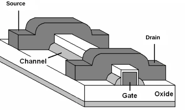
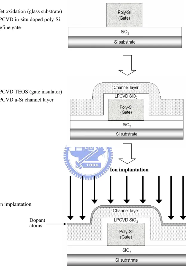
In this chapter, we describe the fabrication of poly-Si TFT with nano-wire channels on the oxidized silicon wafer. We propose a new approach that could potentially resolve the shortcomings mentioned in last chapter. Our approach, albeit based on “top-down” approach, involves only mature and low-cost process skills. Since it could be easily realized using state-of-the-art IC processing, this new scheme is thus very suitable and promising for future practical manufacturing. The three-dimensional graph of the device structure and the top-view layout graph are shown in Fig. 2-1(a)&(b).
2-1-1 Experimental procedures
The schematic illustration of key processes is illustrated in Fig. 2-2. The detailed process flow of poly-Si nano-wire TFT is described as follows:
(1) Zero layer fabrication:
Mark the number on silicon wafers and define the zero-layer alignment key. 1. Use laser marking to define number marks.
2. Perform SC-1 (NH4OH) cleaning to remove the particles.
3. Use stepper (ASM) to define Zero Mark. 4. Use RIE (TEL5000) to etch silicon. 5. P.R. stripping.
1. Perform STD (SC-1,SC-2) cleaning.
2. Grow thermal oxide (wet oxide) as to simulate the “glass” substrate.
(3) Define poly-Si gate:
1. Perform STD (SC-1, SC-2) cleaning.
2. Deposit the in-situ doped poly-Si film with thickness of 100 nm(or 200 nm) in an LPCVD system at 625 .℃
3. Use a g-line stepper to define gate pattern (Mask 1). 4. Dry-etch of poly-Si by TCP-9400.
5. P.R. stripping.
(4) Gate oxide:
1. Perform standard RCA cleaning. 2. Dip in HF. (HF:H2O=1:50)
3. Deposit 35 nm TEOS by LPCVD.
(5) Channel layer deposition:
1. Deposit undoped-amorphous Si film with thickness of 100 nm (or 70 nm, 50 nm) in an LPCVD system at 550 .℃
(6) Solid state crystallization (SPC):
1. Before source, drain, and channel defining, some wafers were re-crystallized at 600 in N℃ 2
ambient for 24 hours in the furnace.
(7) Ion implantation:
1. Ion implantation(no mask): n-channel TFT: P+, 1×1015 cm-2, 10 or 15 keV, tilt=0 p-channel TFT: BF2+, 1×1015 cm-2, 10 or 20 keV, tilt=0
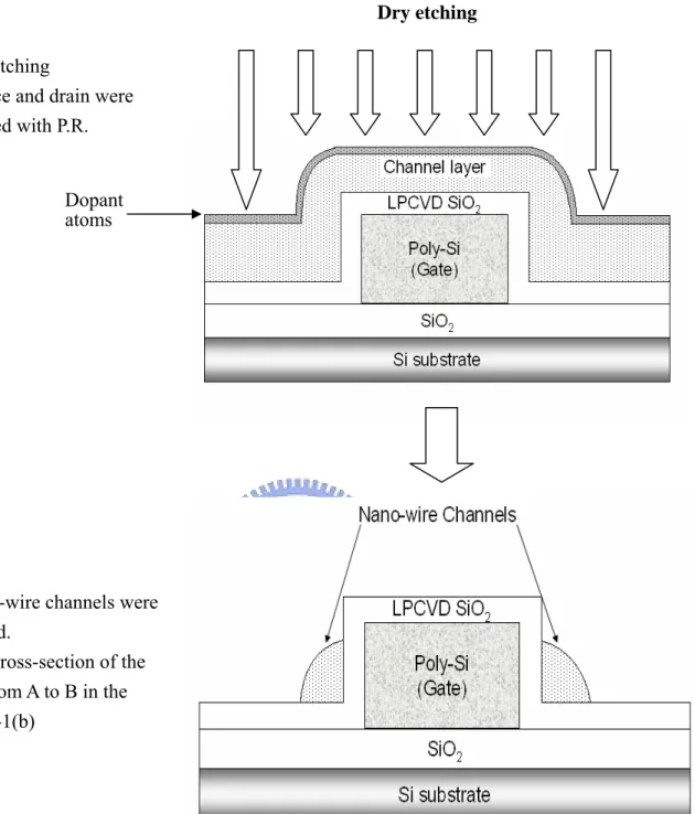
(8) Source, drain, and channel define:
1. Use a g-line stepper to define source, drain, and channel regions (Mask 2). 2. Dry-etch to form sidewall spacer channels by TCP-9400.
3. Use In-line SEM to check the sidewall spacer width. 4. Strip P.R.
(9) Solid state crystallization (SPC):
1. After source, drain, and channel definition, the rest of wafers (not re-crystallized before dry etching) are re-crystallized at 600℃ in N2 ambient for 24 hours in the furnace.
(10) Contact hole formation:
1. Perform STD cleaning.
2. Depositi 200 nm TEOS by LPCVD. 3. Contact hole alignment mask (Mask 3). 4. Wet-etch TEOS by B.O.E.
5. Strip P.R.
(11) Metallization:
1. Dip in HF for 3 seconds.
2. Sputter-deposit 500 nm Al-Si-Cu film. 3. Metal alignment mask (Mask 4). 4. Etch metal by ILD-4100.
5. Strip P.R.
6. Post metal annealing (PMA) at 400 in N℃ 2 ambient for 30 minutes.
(12) Post treatment:
1. Forming gas annealing. (at 400 in 95%N℃ 2 and 5%H2 ambient in the furnace for 30
minutes)
2. NH3 plasma treatment for 1 hour and 2 hours. -End of process-
Note that, in step (7) of the above process flow, source/drain (S/D) implant was performed with low implant-energy, so that most implanted dopants are located near the top surface of the Si layer. S/D P.R. patterns were then formed on the substrate using the G-line
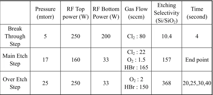
stepper. Table 2-1 shows the etching recipe of the high-density plasma and etching selectivity of poly-Si to SiO2. The etching selectivity in both main etch and over etch steps are larger
than 100, which is suitable for nano-scale patterning. The sidewall Si nano-wire channels were formed in this step in a self-aligned manner. Note that the implanted dopants in places other than S/D regions will be removed during the etching step because of the very shallow projected range just mentioned. The tetraethylorthosilicate (TEOS) layer deposited by LPCVD process has been applied to integrated circuit device fabrication as an inter-metal isolation later and a passivation layer. The deposition of TEOS by LPCVD is at 720 in the ℃ furnace for about 2 hours and the dopants can be activated at this step and the SPC process. After sintering at 400 in N℃ 2/H2 ambient for 30 minutes, the device process was completed.
Some fabricated wafers were subjected to the plasma treatment with condition is shown in Table 2-2. Detailed split conditions are summarized in Table 2-3. The total mask number of the conventional bottom-gate TFTs is five, which is identical to that of conventional etch-stopper TFTs. Comparing to the conventional bottom gate TFTs, the total mask number of our poly-Si NW TFTs is only four.
2-1-2 Experimental results
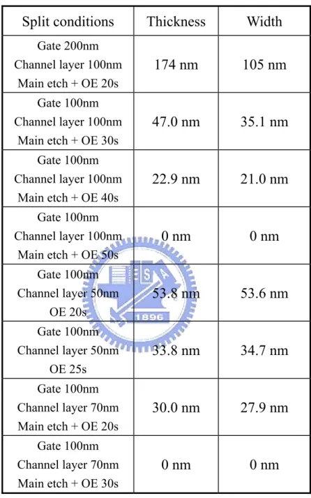
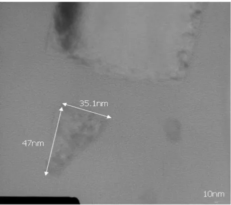
The electrical performance of poly-Si TFTs strongly depends on the width, thickness, and quality of the channel layer. The width and thickness of the sidewall spacer channel both depend on the gate height, thickness of the α-Si channel layer deposition, and etching time for our poly-Si NW TFTs. The definition of the width and thickness of the sidewall spacer channel is shown in Fig. 2-3. Sample(1) was fabricated with 200 nm gate, 100 nm channel layer and 20 seconds over etching. Figures 2-4(a) and (b) shows TEM and SEM pictures of Sample(1), respectively. From Fig. 2-4(a), the thickness and width of the sidewall spacer
nano-wire channel are around 105 nm and 174 nm, respectively, which seem to be too large for the fabrication of nano-wire TFTs. To reduce the nanowire dimensions, gate height as well as the as-deposited channel thickness are reduced. Moreover, over etching time is used as a parameter for the control of the nanowire structure. Figures 2-5~2-11 show the cross-sectional TEM pictures of samples with various gate heights, as-deposited channel layer thickness, and the etching times. The summary of TEM results is listed in Table 2-4. Note in Fig. 2-7 that the sidewall spacer nano-wire channel has been etched off. Figure 2-12 shows that the thickness and width of sidewall spacer nano-wire channel decrease with increasing over etching time as characterized by TEM.
2-2 Operation of poly-Si NW TFT
The operation principles of our new poly-Si NW TFTs are similar to those of the conventional bottom-gate TFTs. For n-channel poly-Si NW TFTs, when the gate and drain are positively biased with respective to the source, and the gate bias is higher than the threshold voltage, the device is turned on. On the other hand, when the gate bias is smaller than the threshold voltage, the device is turned off. In contrast to conventional poly-Si TFTs in term of structural arrangement, our nano-wire channels are aligned along the sidewall of the gate.
The parameters of the transistors and I-V characteristics, including threshold voltage (Vth), linear maximum transconductance (GM), and subthreshold swing (SS), were measured
and extracted. All data were characterized by an HP4156 analyzer. The on-current can be expressed as,
(2-1)
in linear region (for VG > Vth, VG-Vth > VD), where L is the channel length, W is the channel
(
)
1 2 2 D O X G th D D W I C V V V V Lµ
⎡ ⎤ = ⎢ − − ⎥ ⎣ ⎦width, µ is the mobility, and COX is the gate capacitance per unit area. The on-current in
saturation region (for VG > Vth, VG-Vth < VD), can also be expressed as,
(2-2) Then, GM is extracted by the differentiation of equation (2-1),
(2-3)
Subthreshold swing (SS) can be calculated from the subthreshold current increase in the weak inversion region,
(2-4)
These electrical parameters could be extracted from the curve of ID versus VG under a
constant drain voltage of 0.5V.
In this thesis, we use GM(max) (the maximum value of GM) to find Vth. This method is
simple and straight-forward. ON/OFF current ratio is one of the most important performance indicators. In this thesis, we measured the “ON” current at VG=10V, VD=0.5V and VG=-10V,
VD=-0.5V, for n- and p-channel operation, respectively. The “OFF” current was measured at
VG=-3V, VD=0.5V, and VG=3V, VD=-0.5V, for n- and p-channel operation, respectively.
(
)
21
2
D O X G thW
I
C
V
V
L
µ
⎡
⎤
=
⎣
−
⎦
D D M V const O X D GI
W
G
C
V
V
=L
µ
∂
⎛
⎞
=
= ⎜
⎟
∂
⎝
⎠
(
log
V
) (
10
) ( )
V
2.3
(
V
)
G G G D D DSS
ln
I
lnI
lnI
∂
∂
∂
=
=
=
∂
∂
∂
Chapter 3
Characteristics and Discussion of NW TFT
3-1 Device performance
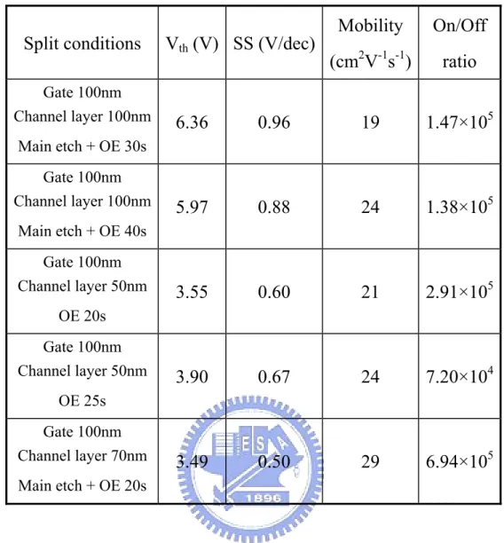
Recently, the poly-Si thin film transistors fabricated by low-temperature process have received extensive study for their important applications to the active matrix liquid crystal display (AMLCD)[30][31]. To optimize the design of the poly-Si NW TFTs with high performance, it is important to develop a reliable analytical methodology based on the physical mechanisms that correlates the electrical characteristics with the fabrication condition. The performance of poly-Si TFTs is dominated by trapping states at grain boundaries and within the grains themselves [32][33]. Although the electron and hole field-effect mobility of poly-Si are considerably higher than those of α-Si, the values are still much lower than those of single-crystal silicon. Fig.3-1 shows the comparison of transfer property between sample(1) and sample(2). Sample(2) has smaller off-state leakage current, larger on-current , and better subthreshlod swing than Sample(1). Figure 3-2 shows the comparison of transfer characteristics between devices with 30 and 40 seconds over-etching time, both with the same gate height (100nm) and channel layer deposition thickness (100nm). However, the device with 40 seconds over-etching 40 time depicts larger off-state leakage current, smaller threshold voltage, and better subthreshlod swing than the device with 30 seconds over-etching time. It is worthy to note that the off-state leakage current of the device with 40s over-etching is larger than that with 30s over-etching. We believe this is because the nano-wire channel with longer-etching time suffered from more plasma damage during the channel-etching step. The mechanisms of off-state leakage current will be discussed in section
3-3. In addition, we also observed that both thinner channel layer and shorter over etching-time affect the characteristics of devices. The comparison on characteristics between the device with 20s over-etching and the device with 25s over-etching, both having the same gate height (100 nm) and channel layer thickness (50 nm), is shown in Fig. 3-3. The comparison on characteristics between the device with 20s over-etching and the device with 25s over-etching, both having the same gate height (100nm) and channel layer thickness (50nm) is shown in Fig. 3-3. The comparison on characteristics between devices with 54nm and 30nm nano-wire thickness is shown in Fig. 3-4. It shows the device with thinner nanowire has smaller threshold voltage and higher drain current, indicating better gate control ability. Detailed summary of characteristic parameters (VD=0.5V) with various channel layer
thickness and etching times is shown in Table 3-1.
The transfer characteristics of SPC-before-etching and SPC-after-etching nano-wire devices are shown and compared in Figs. 3-5(a) and (b). The two figures indicate that the devices with SPC-before-etching nano-wire have better electrical properties. For the device with SPC-after-channel-etching, α-Si was re-crystallized in a confined space, and the grain growth would be easily impeded. As a result, the grain size is smaller than that in the device with SPC before channel etching. The comparison between n-channel and p-channel devices is shown in Fig. 3-6. The characteristics of the n-channel devices are better than that of the p-channel devices, owing to higher electron mobility. The results also indicate that more attentions need to be paid to optimize p-channel devices. Fig. 3-7 shows the threshold voltage of the devices with measurement deviation versus channel length. We can see the process uniformity of poly-Si NW TFTs is less than optimum, and is worse with shorter channel. This is owing to the difficulty in grain size and nanowire dimension control. Fig. 3-8 shows the on-current versus channel length at VG=10V, VD=0.5V. The results in Fig.3-8 basically agree
Another very important electrical characteristic of poly-Si TFTs is ID-VD output
characteristic. The kink effect observed in the drain current of poly-Si TFT operating in the high drain bias regime has been investigated by several works [35-39]. With the aid of two-dimensional (2-D) numerical simulation, the nature of the kink effect had been identified to be due to the impact-ionization mechanism in the high field regime near the drain for the intrinsic poly-Si TFT [35-38]. Along the channel, the formation of the potential barrier of the grain boundary and defects cause the low transconductance and high threshold voltage of poly-Si TFTs. The barrier height is expressed in terms of channel doping, gate oxide thickness, grain size, and external gate as well as drain biases. Drain bias will result in an asymmetric potential barrier and introduce more carrier injection from the lowered barrier side. It is shown that this consideration is very important to characterize the saturation region under high drain bias condition.
Fig. 3-9 and Fig. 3-10 show the ID-VD output characteristics of n-channel devices with
short channel and long channel, respectively. In Fig. 3-9 and Fig. 3-10, the short channel devices exhibit more significant kink effect than long channel devices in the high drain bias region. When the drain bias is applied, the grain barrier heights for both sides of the grain boundary become asymmetric and the grain barrier height of the side near the source junction will be lower than that of the side near the drain junction. Fig. 3-11 shows the energy band diagram along the channel under high drain bias. As a consequence, there will be extra carriers injecting from the source junction through the side with lower grain barrier into the channel, resulting in the increased current. This phenomenon is so called the “drain induced grain barrier lowering” (DIGBL) effect [38]. It is more significant for short channel poly-Si TFTs [39], because the electrons drifting from source to drain is easier for short channel. Impact-ionization effect initiated by DIGBL current is another cause responsible for the kink effect of poly-Si TFTs [40]. When the intrinsic poly-Si TFT operates in the kink regime, the
impact-ionization of carriers occurs in the saturation region in which the lateral electric field is higher than the critical electric field. The impact-ionization mechanism in the saturation region is illustrated in Fig.3-12(a). Fig. 3-12(a) illustrates the multiplication process of the impact-ionization mechanism initiated by the DIGBL current, where ☉ represents the Si atom-site; the arrow with dashed line shows the path of the generated electron-hole pair. The drain-source current includes DIGBL current and impact-ionization current initiated by the electrons. Fig. 3-12(b) illustrates the continuity for the mechanism of the impact-ionization initiated by the DIGBL current. Initially, electrons injecting from the source junction move toward the drain through the transport mechanisms in tandem, by surmounting the grain barriers, diffusing across the depletion regions near the grain boundaries, and drifting through the inversion regions between the depletion regions. This is the transport mechanism described by the interfacial-layer thermionic-diffusion model [41]. The generated electrons and holes, being separated by the high electric field, move toward the drain and source junctions, respectively. When reaching the drain junction, the electron flows originating both from the DIGBL and the impact-ionizations constitute the total drain-source current.
Fig. 3-13 shows the output characteristics of SPC-before-etching and SPC-after-etching samples. The drain current of the devices with SPC-before-etching nano-wire channels are larger than that of the devices with SPC-after-etching nano-wire channels. Figures 3-14(a) and (b) show ID-VD output characteristics of p-channel devices with short channel and long
channel, respectively. It is noted that the drain current of the p-channel device is smaller than that of the n-channel device, both biased at the same absolute values of VG, VD, and channel
length, owing to the lower hole mobility. According to the results above, we summarize that Samples with split conditions (3), (7), and (8) have better transfer properties, and the characteristics of devices with SPC-before-etching channel are better than those of devices with SPC-after-etching channel. In the next section, we will discuss how to improve the
device characteristics.
3-2 Effects of post treatment
It is well known that the grain boundaries exert a profound influence on device characteristics, because electronic charges trapped within grain boundaries form potential barriers. Due to the high density of defect states at grain boundaries and interior of grains, poly-Si TFTs exhibit poor performance such as low mobility, large subthreshold swing, large threshold voltage, and large leakage current, compared to single-crystal counterparts. Therefore, to minimize the defect density in polysilicon film is essential to realizing high performance TFTs.
Hydrogen plasma passivation of polysilicon films to reduce defect states in the grains and the grain boundaries has been widely investigated for improving the electrical characteristics of polysilicon thin film transistors [42-45]. The hydrogen plasma treatments can improve the performance of poly-Si TFTs by lowering the grain boundary potential barriers [44][45]. It is well-known that hydrogenation tends to tie up the grain boundary dangling bonds and intra-grain strain bonds with hydrogen, thereby remarkably improving the characteristics of the poly-Si TFTs [44][45]. After plasma passivation, better performance including higher on/off current ratio, higher field-effect mobility, higher drive current, lower leakage current, lower threshold voltage, and lower subthreshold swing can be achieved. The effects of forming gas annealing and NH3 plasma treatment on the subthreshold
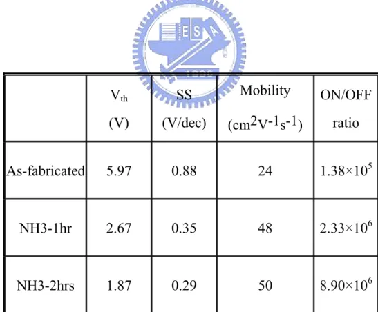
characteristics are shown in Fig.3-15 and Table 3-2. After forming gas annealing 30 mins, the characteristics of device can be improved, including higher on-current, lower off-state current, higher mobility, larger On/Off current ratio, lower subthreshold voltage, and better subthreshold swing. After NH3 plasma treatment, the characteristics of the device are much
improved over the as-fabricated and forming-gas-annealed devices. We have also extended the NH3 plasma treatment time, and observed the effect on electrical characteristics. Figures
3-16 and 3-17 show the device characteristics of as-fabricated sample and samples after either 1-hour or 2-hour NH3 plasma treatments. In Fig.3-17, it can be seen that longer NH3 plasma
treatment time results in further improvement of the device characteristics. It is ascribed to more defect passivation in the films by longer NH3 plasma treatment time. Detail device
characteristics of as-fabricated sample and samples with either 1-hour or 2-hour NH3 plasma
treatment are shown in Table 3-3. In Fig.3-18, it can be seen that, after NH3 plasma treatment,
the device characteristics are similar for devices with channel layer SPC either before or after plasma, indicating that extra defects are efficiently passivated by NH3 plasma treatment. In
Figs. 3-19(a) and (b), drain current of the device after NH3 plasma treatment is larger than that
of the as-fabricated device, and the kink effect is significantly suppressed after NH3 plasma
treatment, regardless of the channel length. This implies that the passivation of defect states could effectively suppress the DIGBL current.
3-3 Origins of leakage current
Polysilicon thin-film transistors have been actively investigated for use in peripheral and active-matrix circuits in large-area liquid crystal display because of their high field-effect mobility and reliability. However, compared to amorphous silicon TFTs, poly-Si TFTs suffer from larger off-state leakage current, which could render them unacceptable for pixel driver application. In order to hold the signal at levels for acceptable image quality, the off-state current must be reduced to well below 1 pA/µm. Considerable effort has been devoted to clarifying the conduction mechanisms of off-state leakage current in poly-Si TFTs since the 1980’s, such as field emission, field-enhanced thermal emission, resistive current and
conduction mechanism of off-state leakage current is dominated by one of those proposed mechanisms. Recently, it has been found that the mechanisms of off-state current are dependent on gate bias, drain bias, device size, device structure, and fabrication conditions such as process temperature, annealing condition, hydrogenation, thickness of active poly-Si layer, and deposition method of gate insulator. In short, the leakage current is not due to a simple mechanism. In addition to the mechanisms referred to above, there are other contributions to the off-state leakage current depending upon the overall trap density and the extent to which it has been passivated as well as the film thickness and grain size effects. When a negative gate bias (VG) is applied to an n-channel TFT, there will be considerable
off-state leakage current which results from two basic mechanisms [46].
1. Resistive current: in this case the applied VG is not negative enough to induce a p-layer in
the channel surface region, so the off-stare leakage current can be assumed to be an ohmic current through the poly-Si layer.
2. Junction leakage current: when VG is more negative, a significantly reverse-biased pn
junction is formed near the channel interface between the drain and channel. The junction leakage current is carried by the holes generated via grain boundary traps in the depletion region.
First, we consider the effect of plasma damage on the off-state leakage current for our poly-Si NW TFTs. In Fig.3-20, the device with longer plasma etching time exhibits higher off-state leakage for devices with SPC before etching. It is presumably due to plasma etching-induced damage on the nano-wire channel. On the other hand, reduction in the off-state leakage current with longer etching time is observed for devices with SPC after etching. It is ascribed to the fact that the SPC after etching can remove part of the plasma damage during nano-wire channel etching step. In this case, the longer etching time results in smaller cross-sectional area of the nanowire, and thus lower leakage current. It is important to
note that the off-state leakage current of the SPC-after-etching device is still higher than the SPC-before-etching device. Moreover, the transfer characteristics of the SPC-after-etching device are not better over those of the SPC-before-etching device. It may be due to the smaller grain size of the channel layer for the device with SPC-after-etching, as mentioned in previous section. The off-state leakage current as a function of VG and VD is shown in Figs. 3-21(a)
and (b). Higher drain bias results in higher off-state leakage current. Furthermore, the more negative the gate bias, the higher the off-state leakage current. In order to further discuss the reason of off-state leakage current, we have to understand the activation energy in the off-state region. The activation energy of the off-state can be obtained from the temperature dependence of the drain current. The governing equation of off-state current, activation energy, and temperature is given by
a E -k T o ff 0 I = I e (3-1), where I0 = constant independent of temperature, and Ea = drain current activation energy.
The equation also can be expressed as
a off 0 -E log (I )=log(I )+ kT ⎛ ⎞ ⎜ ⎟ ⎝ ⎠ (3-2).
The off-state currents with various temperatures (25℃, 50℃, 75℃, 100℃, and 125℃) are shown in Fig. 3-22(a). Next, we use equation (3-2) to plot the Arrhenius plot, which is shown in Fig. 3-22(b). The activation energy (Ea) can be extracted from the slope of the data lines
[47]. Figure 3-23(a) shows the dependence of Ea on gate and drain voltages. Either more
negative gate bias or higher drain bias can reduce the activation energy, and results in larger off-state leakage current. In Fig. 3-23(b), the activation energy of the device with NH3 plasma
treatment is higher than that of as-fabricated device at high gate and drain voltages. It is suggested to be due to the fact that NH3 plasma can effectively passivate the defects and trap
given constant gate voltage. Under lower drain bias, Ea keeps roughly a constant value about
0.5eV (~ Eg/2). Two possible mechanisms are proposed to account for the off-state leakage
current for our devices.
Mechanism 1:
This mechanism considers the trap-assisted conduction processes occurring laterally from channel to the drain. There are three related cases illustrated in (a), (b), and (c) of Fig. 3-24.
(a) Pure thermal emission or thermal generation: this is duo to thermal excitation of an electron from valence band into trap-state, and the trapped electron is emitted to the conduction band by the same way.
(b) Thermionic field emission: this is due to the field-enhanced emission under a medium electric-filed strength. This case comprises two steps in tandem: the first step is the thermal activation of an electron from the valence band to a trap state, and the second step is electron tunneling through the reduced barrier to the conduction band as shown in Fig. 3-24(b).
(c) Field emission or tunneling: under a strong electric field, the band gap is pulled more severely. It causes the electrons to tunnel from the valence band to the conductance band via the trap states.
All the processes stated above are common to poly-Si thin film transistors with top-gate self-aligned structure, and the presence of trap state in the band-gap plays an important role. The trap-assisted field emission current has the strongest dependence on the applied bias, but is essentially independent of temperature, thus it is dominant under low-temperature and/or high-field conditions. The thermal emission current is proportional to the intrinsic carrier concentration of silicon (ni) which is proportional to exp[-Eg/2kT] (where Eg is the energy
band gap of silicon, k is the Boltzmann constant, and T is temperature in Kelvin). For this reason, the activation energy of the pure thermal emission current should be approximately equal to Eg/2. In addition, the pure thermal generation current is nearly independent of gate
voltage.
Mechanism 2:
In Fig. 3-25, it highlights the unique gate-drain overlap region that defines the top gate width of our device. The off-state current for different gate widths is shown in Figs. 3-26(a) and (b). As can be seen in the figures, the off-state current is actually proportional to the gate width, implying that the conduction path is located in the gate-drain overlap regions illustrated in Fig.3-25. We also extracted the activation energy for devices with gate width of 5 and 1 µm, respectively. The results are shown in Fig. 3-27. It can be seen that the activation energy is essentially independent of the gate width at both VD=0.5V and VD=5V, indicating
the same conduction mechanism is responsible for the samples, and it occurs in the gate-drain overlap region. Fig. 3-28 illustrates the band diagrams of three cases in the gate-drain overlap region for mechanism 2 proposed to explain the leakage current conduction:
(a) Low electric field: in this situation, both gate and drain bias are low. Therefore, the off-state current is dominated by thermal emission.
(b) Medium electric field: the electrons in the valence band are thermally activated to the trap states, and then tunnel to the conduction band. This is known as the thermionic field emission.
(c) High electric field: under this situation, quasi Fermi level at the channel/oxide interface shifts nearer to valence band edge, and band-to-band tunneling takes place easier with the aid of trap states, which may lead to a high leakage current in the off-state region.
in Fig.3-27, and the resulted current is proportional to the gate-to-drain overlap width indicated in Fig.3-26. This conduction mechanism is thus believed to be responsible for the off-state leakage characterized in this work.
Chapter 4
Conclusions and Future Works
4-1 Conclusions
In this work, a novel poly-Si NW TFT device and its fabrication method are proposed. The overall process of this device is very simple, fast, and cheap. In this approach, we can obtain the sidewall spacer nano-wire by channel layer etching. Critical dimensions of the nano-wires can be adjusted by setting appropriate gate height, channel layer thickness, and etching time.
In this work, the novel NW device is successfully demonstrated. Reasonable performance of the fabricated device is obtained, and could be dramatically improved using NH3 plasma treatment. For example, high On/Off current ratio of near 107 is obtained. In
addition, we analyzed and discussed the origins of the off-state leakage current. It is also identified that the gate-to-drain overlap region determines the off-state leakage. Based on this finding, further improvement on reducing the leakage current is possible by appropriately modifying the device’s structural parameters and the process conditions.
Table 4-1 highlights the major advantages of the proposed scheme. This technique is manufacturable and economic, and is capable of providing a reliable high-performance poly-Si NW TFTs which are not only useful for biosensors but also for investigating nano-scale semiconductor physics. It is also compatible with the low-temperature poly-Si (LTPS) technologies, and could be integrated on low-cost and flexible substrates (such as glass or plastic), making the fabrication of system-on-panel (SOP) for biologic sensing and regulating purpose products possible.
4-2 Future works
Polycrystalline silicon is rich in grain boundary defects as well as intragrain defects, and the electrical activity of these charge-trapping centers profoundly affects the TFT characteristics. To further improve the device performance, it is important to reduce the defects and trap-states in poly-Si film for the poly-Si NW TFT. This could be achieved by using the MILC or ELC to enlarge the grain size of the poly-Si films.
Another important work is to reduce the off-state current with optimized device layout and structure. Furthermore, we may use other materials like the poly-Ge film to potentially enhance the carrier mobility, and the silicide material for S/D to reduce the parasitic resistance. With suitable optimization, we believe that the performance of poly-Si NW TFTs can be improved significantly. As long as decent performance is achieved, the new NW device can be readily applied to a variety of novel applications in the future.
References
[1] Ichio Yudasaka et al. “Polysilicon Thin-Film Transistors”, Mat Res. Soc. Symp. Proc., pp.162, vol.182, 1990.
[2] S. Wolf and R. N. Tauber, “Silicon Processing for the VLSI Era”, Lattice Press, California, vol.1, chap.6, pp.161, 1986.
[3] S. D. Brotherton, “Polycrystalline Silicon Thin Film Transistors”, Semicond. Sci. Technol., 10, 1995.
[4] C. H. Fa and T. T. Jew, “The Polysilicon Insulated-Gate Field-Effect Transistors”, IEEE Trans. Electron Devices, vol.13, no.2, pp.290, 1966.
[5] G. Baccarani, B. Ricco and G. Spadin, “Transport Properties of Polycrystalline Silicon Films”, J. Appl. Phys., vol.49, pp.5565, 1978.
[6] I-Wei Wu, Alan G. Lewis, Tiao-Yuan Huang, Warren B. Jackson and Anne Chiang, “Mechanism and Device-to-Device Variation of Leakage Current in Polysilicon Thin Film Transistors”, IEDM 1990, pp.867-870.
[7] P. Migliorate, “Progress in Active Matrix Addressing of LCDs”, in Pro. Int. Display Res. Conf., pp.44, 1987.
[8] Masanori Yuki, Kunio Masumo, and Masaya Kunigita, “A Full-Color LCD Addressed by Poly-Si TFTs Fabricated Below 450 ”, IEEE Transaction on Electron Devices, vol.36, ℃ no.9, pp.1934-1937, 1989.
[9] A. G. Lewis, David D. Lee and R. H. Bruce, “Polysilicon TFT Circuit Design and Performance”, IEEE J. Solid-State Circuit, vol.27, no.12, pp.1833, 1992
[10] T. Morita, Y. Yamamoto, M. Itoh, H. Yoneda, Y. Yamane, S. Tsuchimoto, F. Funadda and K. Awane, “VGA Driving with Low Temperature Processed Poly-Si TFTs”, IEDM Tech. Dig. pp.841, 1995.
[11] M. J. Edwards, S.D. Brotherton, J. R. Ayres, D.J. McCulloch and J. P. Gowers, “Laser Crystallized Poly-Si Circuits for AMLCDs”, Asia Display, pp.335, 1995.
[12] Shunji Seki, Osamu Kogure, and Bunjiro Tsujiyama, “Effects of Crystallization on Trap State Densities at Grain Boundaries in Polycrystalline Silicon”, IEEE Electron Device Lett., vol.8, pp.368-370, August 1987.
[13] T. W. Little, K. I. Takahara, H. Koike, et al, “Low Temperature Poly-Si TFTs Using Solid Phase Crystallization of Very Thin Films and an Electron Cyclotron Resonance Chemical vapor deposition gate insulator”, Jpn. J. Appl., Phys., vol.30, no.12B, pp.3724-3728, December 1991.
[14] Hiroyuki Kuriyama, Seiichi Kiyama, Shigeru Nouguchi, et al, “Enlargement of poly-Si Film Grain Size by Excimer Laser Annealing and its Application to High-Performance Poly-Si Thin Film Transistor”, Jpn. J. Appl. Phys., vol.30, no.12B, pp.3700-3703, December 1991.
[15] S. W. Lee and S.K. Joo, “Low Temperature Poly-Si Thin Film Transistors Fabrication by Metal-Induced Lateral Crystallization”, IEEE Electron Device Lett., vol.17, no4, pp.160-162, April 1996.
[16] M. K. Hatalis and D.W. Greve, “High Performance Thin Film Transistors in Low-Temperature Crystallized LPCVD Amorphous Silicon Films”, IEEE Electron Device Lett., vol.8, pp.361-364, 1987.
[17] Mingxiang Wang, Zhiguo Meng, and Man Wong, “Anisotropic Conduction Behavior in Metal-Induced Laterally Crystallized Polycrystalline Silicon Thin Films”, Appl. Phys. Lett., Vol.76, pp.448, 2000.
[18] S. D. Brotherton, D. J. McCulloch, J. P. Gowers, and A. Gill, “Laser Crystallized Poly-Si TFTs”, Microelectron. Eng., vol.19, pp.101-104, 1992.
[19] Byung-Seong Bae and Choochon Lee, “Effect of Interface State Distribution on Field Effect Conductance Activation Energy in Hydrogenated Amorphous Silicon Thin Film
transistors”, J. Appl. Phys., vol.88, pp.3439-3442, 1990.
[20] M. J. Powell, J. Pritchard, “The Effect of Surface States and Fixed Charge on the Field Effect Conductance of Amorphous Silicon”, J. Appl. Phys., vol.54, pp.3244-3248, 1983. [21] H. C. Lin and S. M. Sze, “Nanoelectronic Technology: in Search of the Ultimate Device
Structure,” in Future Trends in Microelectronics: the Nano Millennium, S. Luryi, J. M. Xu, and A. Zaslavsky, eds., pp.4-14 (New York: Wiley 2004).
[22] Duan. X., Huang. Y., Lieber. C. M. “ Nonvolatile Memory and Programmable Logic from Molecule-Gated Nanowires”, Nano Letters, Vol.2, No.5, pp.487-490, 2002
[23] Xiangfeng Duan, Chunming Niu, et al, “High-Performance Thin-Film Transistors Using Semiconductor Nanowires and Nanoribbons”, Nature, Vol.425, pp.274-278, 2003.
[24] Yi Cui, Qingqiao Wei, Hongkun Park, and Charles M. Lieber, “Nanowire Nanosensors for Highly Sensitive and Selective Detection of Biological and Chemical Species”, Science, Vol.293, pp.1289-1292, 2001.
[25] Alfredo M. Morales and Charles M. Lieber, “A Laser Ablation Method for the Synthesis of Crystalline Semiconductor Nanowires”, Science, Vol.279, pp.208-211., 1998
[26] Dunwei Wang, Qian Wang, et al., “Germanium Nanowire Field-Effect Transistors with SiO2 and High-k HfO2 Gate Dielectrics”, Appl. Phys. Lett., Vol.83, pp. 2432-2434, 2003
[27] N. Wang, Y. F. Zhang, Y. H. Tang, et al., “SiO2-Enhanced Synthesis of Si Nanowires by
Laser Ablation”, Appl. Phys. Lett., Vol.73, pp.3902-3904, 1998.
[28] Xiangfeng Duan, Yu Huang, Yi Cui, et al. “Indium Phosphide Nanowires as Building Blocks for Nanoscale Electronic and Optoelectronic Devices”, Nature, Vol.409, pp.66-69, 2001.
[29] Yu Huang, Xiangfeng Duan, Qingqiao Wei, and Charles M. Lieber, “Directed Assembly of One-Dimensional Nanostructures into Functional Networks”, Science, Vol.291, pp.630-633, 2001.
Peripheral Poly-Si TFT Circuits”, IEDM Tech. Dig., pp.289-392, 1993.
[31] T. Aoyama, K. Ogawa, et al, “Inverse Staggered Poly-Si and Amorphous Si Double Structure TFT’s for LCD Panels with Peripheral Driver Circuit Integration”, IEEE Trans. Electron Devices, vol.43, pp.701-705, May 1996.
[32] G. Baccarani, B. Ricco and G. Sadin, “Transport Properties of Polycrystalline Silicon Films”, J. Appl. Phys., vol.49, pp.5565, 1978.
[33] P. Migliorato and D. B. Meakin, “Mateaial Properties and Characteristics of Polysilicon Transistors for Large Area Electronics”, Appl. Surf. Sci., vol.30, pp.353, 1987.
[34] M. Validinoci, L. Colalongo, et al, “Floating Body Effects in Polysilicon Thin-Film Transistors”, IEEE Trans. Electron Devices, vol.44, pp.2234-2241, Dec. 1997.
[35] G. A. Armstrong, S. D. Brotherton, and J. R. Ayres, “A Comparison of the Kink Effect in Polysilicon Thin Film Transistors and Silicon on Insulator Transistors”, Solid-State Electron., vol.39, no.9, pp.1137-1346, Sept. 1996.
[36] M. Hack, J. G. Shaw, et al, “Numerical Simulations of Amorphous and Polycrystalline Silicon Thin-Film Transistors”, Jpn. J. Appl. Phys., vol.29, no.12, pp.2360-2362, 1990. [37] S. Yamada, S. Yokoyama, and M. Koyanagi, “Two-Dimensional Device Simulation for
Polycrystalline Silicon Thin-Film Transistor”, Jpn. J. Appl. Phys., vol.29, no.12, pp.2388-2391, 1990.
[38] P. S. Lin, J. Y. Guo, and C. Y. Wu, “A Quasi-Two-Dimensional Analytical Model for the Turn-on Characteristics of Polysilicon Thin-Film Transistors”, IEEE Trans. Electron Devices, vol.37, pp.666-674, Mar. 1990.
[39] So Yamada, Shin Yokoyama and Mistumasa Koyanagi, “Two-Dimensional Device Simulation for Avalanche Induced Short Channel Effect in Poly-Si TFT”, IEEE, IEDM, pp.859-862, 1990.
[40] Hsin-Li Chen, Ching-Yuan Wu, “A New I-V Model Considering the Impact-Ionization Effect Initiated by the DIGBL Current for the Intrinsic n-Channel Poly-Si TFT’s ”, IEEE
Trans. Electron Devices, vol.46, no.4, pp.722-728, 1999.
[41] C.-Y. Wu and W.-D. Ken, “A New Computer-Aided Simulation Model for Polycrystalline Silicon Film Resistors”, Solid-State Electron., vol.26, no.7, pp.675-684, 1983.
[42] Shunji Seki, Osamu Kogure, and Bunjiro Tsujiyama, “Effects of Crystallization on Trap State Densities at Grain Boundaries in Polycrystalline Silicon”, IEEE Electron Device Lett., vol.8, no.8, pp.368-370, August 1987.
[43] T. J. King, M. G. Hack, and I-Wei Wu, “Effective Density-of-States Distributions for Accurate Modeling of Polycrystalline-Silicon Thin-Film Transistors”, J. Appl. Phys., vol.75, no.2, pp.908-913, 15 January 1994.
[44] B. A. Khan and R. Pandya, “Activation-Energy of Source-Drain Current in Hydrogenated and Unhydrogenated Polysilicon Thin-Film Transistors”, IEEE Trans. Electron Devices, vol.37, pp.1727-1734, 1990.
[45] I. W. Wu, T. Y. Huang, W. B. Jackson, A. G. Lewis and A. C. Chiang, “Passivation kinetics of Two Types of Defects in Polysilicon TFT by Plasma Hydrogenation”, IEEE Electron Device Lett., vol.12, no.4, pp.181-183, April 1991.
[46] Ching-Fa Yeh, Tzung-Zu Yang, Chun-Lin Chen, et al, “Experimental Comparison of Off-State Current between High-Temperature and Low-Temperature-Processed Undoped Channel Polysilicon Thin-Film Transistors”, Jpn. J. Appl. Phys., vol.32, no.10, pp.4472-4478, October, 1993.
[47] K. R. Olasupo and M. K. Hatalis, “Leakage Current Mechanism in Sub-Micron Polysilicon Thin-Film Transistors”, IEEE Trans., Electron Devices, vol.43, no.8, 1996. [48] I.-W. Wu, A. G. Lewis, T.-Y. Huang, and A. Chiang, “Effects of Trap-State Density
Reduction by Plasma Hydrogenation in Low-Temperature Polysilicon TFT”, IEEE Electron Device Lett, vol.10, no.3, pp.123-125, 1989.