國
立
交
通
大
學
電子工程學系 電子研究所
博 士 論 文
先進
CMOS 元件結構的解析模型建立⎯量子侷限效應及
製程變異敏感度之探討
Analytical Modeling of Advanced CMOS Device Structures ⎯
Quantum Confinement and Sensitivity to Process Variations
研 究 生:吳育昇
指導教授:蘇 彬 教授
先進
CMOS 元件結構的解析模型建立⎯量子侷限效應及
製程變異敏感度之探討
Analytical Modeling of Advanced CMOS Device Structures ⎯
Quantum Confinement and Sensitivity to Process Variations
研 究 生:吳育昇 Student:Yu-Sheng Wu
指導教授:蘇 彬 Advisor:Pin Su
國 立 交 通 大 學
電子工程學系 電子研究所
博 士 論 文
A DissertationSubmitted to Department of Electronics Engineering and Institute of Electronics
College of Electrical and Computer Engineering National Chiao Tung University
in partial Fulfillment of the Requirements for the Degree of
i
先進
CMOS 元件結構的解析模型建立
⎯量子侷限效應及
製程變異敏感度之探討
研究生:吳育昇
指導教授:蘇彬 博士
國立交通大學 電子工程學系 電子研究所
摘要
本論文建立一個理論架構,以Poisson 和 Schrödinger 方程式的解析解為基礎,考慮 量子侷限效應,探討多種先進元件結構的微縮性及對於製程變異的敏感度。這個理論架 構包含多重閘極元件(Multi-Gate)、環閘極元件(Gate-All-Around)、超薄層通道元件 (Ultra-Thin-Body)等先進元件結構,並可應用於使用高遷移率(high mobility)通道材料的 元件。 利用三維 Poisson 方程式的解析解,我們可由靜電完整性的角度,比較多重閘極元 件及環閘極元件的臨界電壓對於製程變異的敏感度。結論指出採用輕摻雜通道的環閘極 元件受到製程變異及隨機摻雜擾動的影響最小。對於重摻雜通道的元件,摻雜數目的變 異 會 決 定 元 件 的 臨 界 電 壓 變 異 , 而 環 閘 極 元 件 由 於 其 較 大 的 表 面 積- 體 積 比 (surface-to-volume ratio),其臨界電壓受到摻雜數目變異的影響將會大於多重閘極元件。 當元件尺度更加微縮,我們利用 Schrödinger 方程式的解析解,探討量子侷限效應 對於短通道元件鰭狀電晶體及環閘極元件的臨界電壓變異的影響。結論指出,由於量子 侷限效應,通道寬度變異對於極小尺寸的鰭狀電晶體及環閘極元件的重要性提升。對於 採用不同通道表面方向鰭狀電晶體而言,(100)表面方向的矽元件及(111)表面方向的鍺元 件在通道寬度變異時,表現出較低的臨界電壓敏感度。由於臨界電壓對通道寬度的敏感 度會由短通道效應及量子侷限效應共同決定,因此環閘極元件的通道寬度可經由最佳化設計以減少臨界電壓變異。
利用 Schrödinger 方程式的解析解,我們探討量子侷限效應對於超薄層通道元件及
多重閘極元件的短通道效應的影響。結論指出,當元件的通道厚度小於某一臨界值時, 量子侷限效應可改善超薄層鍺元件的臨界電壓下降(threshold voltage roll-off)。由於鍺通 道較為顯著的量子侷限效應,超薄層鍺元件可能比矽元件有更小的臨界電壓下降。對於 多重閘極結構,砷化銦鎵(InGaAs)通道的臨界電壓下降問題可被鰭狀通道高度(fin height) 方向的量子侷限效應抑制,使其與鍺通道元件相比有更小的臨界電壓下降。此二維的量 子侷限效應對於多重閘極元件的微縮性有顯著的影響。我們改變通道寬度及高度,觀察 不同高寬比(aspect ratio)的元件,發現當元件的 subthreshold swing 相同時,三閘極(Tri-gate) 電晶體由於其較顯著的二維量子侷限效應,比鰭狀電晶體(FinFET)有更佳的微縮性。 我們提供一個適用於高介電閘極絕緣層平坦式矽及鍺通道元件的量子侷限效應形 成的載子層厚度(dark space)的封閉形式(closed-form)模型。這個模型對於(絕緣層及通道 間)能障高度、表面電場、通道及閘極絕緣層中的等效質量等參數的相依性皆有良好的 準確度。此模型亦適用於通道採用後退型摻雜(retrograde doping)的元件。此模型可應用 於預測鍺元件考慮量子侷限效應後的subthreshold swing 及臨界電壓上升量。由於量子侷 限效應會放大摻雜擾動造成的臨界電壓變異,我們進一步建立了此量子侷限效應造成的 倍增因數模型。利用此量子模型,我們可以更準確地評估各個參數(如有效氧化層厚度 (EOT)、溫度等)對於摻雜擾動造成的臨界電壓變異的影響。
應用等效趨動電流法(effective drive current approach),可分析隨機摻雜擾動(RDF) 及線邊緣粗糙(LER)對於平坦式 Bulk 元件及鰭狀電晶體(FinFET)的切換時間(switching
iii
關鍵字:臨界電壓變異、量子侷限效應、超薄層通道元件、多重閘極元件、環閘極元件、 高遷移率元件、切換時間
Analytical Modeling of Advanced CMOS Device Structures-
Quantum Confinement and Sensitivity to Process Variations
Student:
Yu-Sheng
Wu Advisor:
Dr.
Pin
Su
Department of Electronics Engineering and
Institute of Electronics
National Chiao Tung University
Abstract
Based on the analytical solution of Poisson and Schrödinger equation, this dissertation establishes a theoretical framework to investigate the device scalability and sensitivity to process variations considering the impact of quantum-confinement effects. This theoretical framework includes advanced CMOS device structures such as multi-gate, and Gate-All-Around (GAA), and Ultra-Thin-Body (UTB) devices, and can be applied to devices with high-mobility channel materials.
From the prospective of electrostatic integrity, we compare the sensitivity of threshold voltage (Vth) to process variations for multi-gate devices with various aspect ratio (AR) and
v multi-gate MOSFETs.
Using the derived analytical solutions of Schrödinger equation for short-channel devices, we investigate the impact of quantum-confinement effect on the sensitivity of Vth to process
variations. Our study indicates that, for ultra-scaled FinFET and GAA devices, the importance of channel thickness (tch) variation increases due to the quantum-confinement effect. For
FinFET, the Si-(100) and Ge-(111) surfaces show lower Vth sensitivity to the tch variation as
compared with other orientations. As the Vth sensitivity to tch for short-channel device is
determined by the short-channel effect and the quantum-confinement effect, the tch of GAA
MOSFETs can be optimized to reduce the Vth variation.
The impact of quantum-confinement on the short-channel effect for UTB and multi-gate MOSFETs are investigated using the derived analytical solutions of Schrödinger equation. When the tch is smaller than the critical thickness, the quantum-confinement effect may
decrease the Vth roll-off of GeOI MOSFETs. Thus, Ge devices may exhibit better Vth roll-off
than the Si counterpart because of the more significant quantum confinement. For multi-gate structure, by exploring the quantum-confinement effect along the Hfin direction, the Vth
roll-off of InGaAs devices can be suppressed and become smaller than the Ge counterpart. This 2-D quantum-confinement effect is also crucial to the scalability of multi-gate device. Our study indicates that for a given subthreshold swing, Tri-gate (AR=1) with significant 2-D confinement effect exhibits better Vth roll-off than FinFET (AR>1).
We provide a closed-form model of quantum “dark space” for Ge and Si MOSFETs with high-k gate dielectric. This model shows accurate dependences on barrier height, surface electric field, and quantization effective mass of channel and gate dielectric. Our model can also be used for devices with the steep retrograde doping profile. This physically accurate dark space model will be crucial to the prediction of the subthreshold swing and quantum-confinement induced Vth shift of advanced Ge devices. Using this closed-form dark
space model, we also provide a closed-form model for the quantum-confinement induced amplification factor (AFQC) in Vth variation due to random dopant fluctuation (RDF). Using
our model, various factors such as EOT and temperature that may modulate/reduce the impact of RDF on Ge and Si MOSFETs can be accurately assessed.
The impact of RDF and LER on the switching time variations of bulk MOSFETs and FinFET have been assessed using the effective drive current approach that decouples the switching time variation into transition charge (∆Q) and effective drive current (Ieff) variations.
Our results indicate that for bulk MOSFETs, although the RDF has been recognized as the main variation source to Vth variation, the relative importance of LER increases as the
switching time variation is considered. As for lightly-doped FinFET, although the impact of fin-LER is more crucial to Vth variation, the relative importance of gate-LER increases as the
switching time variation is considered.
Keywords: threshold voltage variation, quantum-confinement, Ultra-Thin-Body, Multi-Gate, Gate-All-Around, high mobility channel, switching time
vii
誌謝
進入交大以來漫長而充實的旅程,如今即將抵達終點。在碩博兩階段共七年多的時 間,是養成我專業能力的精華時期,這段研究生涯中,感謝蘇彬老師多年的指導,拓展 了我的研究視野以及培養我對問題的思考邏輯。老師總能未雨綢繆地考量到未來所需, 一步步地建構起研究環境。在無數次和老師的討論中,不斷激發出新的想法,也慢慢勾 勒出這本論文的雛形。每次完成的研究片段要發表時,老師總是再三斟酌修改字句,以 期能更準確地表達出研究內容。當投稿不順利令我士氣受沮時,老師的客觀分析總能讓 我重拾信心,有動力再繼續嘗試。如今這幾年的研究成果能夠集結而成這篇論文,首先 要謝謝老師的督導和鼓勵。 最後階段的畢業口試終於得以順利通過。感謝汪大暉教授擔任口試召集人,以及林 鴻志教授、趙天生教授、李佩雯教授、楊富量主任在百忙之中抽空來擔任我的口試委員, 耐心回覆我在邀集過程中的多次叨擾,並且提供我許多的寶貴建議。在我的口試當天, 感謝實驗室成員幫忙事前準備,也謝謝電機學院的廖郁雁小姐,對於口試場地的借用以 及行政事務的鼎力協助。 從碩士班時就一直欣羨著李維、陳柏年、王生圳三位學長的背影,或許這也是當時 促使我想繼續唸博士班的動機之一,很感謝你們提供的建議與經驗分享。同時和我進 入實驗室的 Vita 和俊延,我們是一同經歷過各個大小戰役的老兵,很高興最終都能順 利通過考驗,一起完成博士學業。銘隆、昆諺、昌鴻三位博班學弟,有你們的幫忙, 這本論文中的許多部分才得以完成,你們也讓我的生活點綴了許多有趣回憶。已畢業 的欣原,感謝你對我的個人電腦的照料以及研究上的幫助。在和劭衡、俊賢、青維、 克駿相處時,常會讓我想起碩士班時的生活,和你們的閒聊也常讓我驚覺我們年齡上 的差異。謝謝嘉塵學弟、孟漢、明琦,你們常常熱心分享博士班的生活點滴,為我們 增添了許多話題。 謝謝我的家人,這幾年一直支持我繼續博士學業,提供我生活上和心理上的強力後盾,在我遭受挫折時安慰我,在我通過難關時分享我的喜悅。感謝秉真的陪伴,少了 你,我的生活將只是單調的例行記事,除了在課業研究外,還鼓勵我多方面去嘗試新 的興趣,讓我對於研究和生活更有熱情。此外,謝謝你在口試前的最後階段還充當聽 眾,幫助我修飾講述內容。 這本論文的完成還要感謝國家高速網路與計算中心長期提供學術界模擬軟體的 license,讓我的理論計算得以進行驗證。另外,李素萍小姐和黎裕群學長提供的協助, 讓我們能更有效率地解決軟體使用的問題。我的研究需要倚賴實驗室的工作站,都是 由銘隆和劭衡負責維護和管理,這繁重的工作讓我由衷地欽佩與感謝。 2011 年十一月 誌于交通大學
ix
Contents
摘要
...IABSTRACT
...IV誌謝
... VII CONTENTS ...IX TABLE CAPTIONS...XIII FIGURE CAPTIONS...XIVCHAPTER 1 INTRODUCTION
... 1CHAPTER 2 SENSITIVITY OF THRESHOLD VOLTAGE TO PROCESS
VARIATIONS-A PERSPECTIVE FROM ELECTROSTATIC
INTEGRITY
... 62.1INTRODUCTION... 6
2.2MODELING OF SUBTHRESHOLD CHARACTERISTICS FOR MULTI-GATE AND GAA
STRUCTURES... 7
2.2.1 Analytical Channel Potential Solution for Multi-Gate Structure ... 7 2.2.2 Analytical Channel Potential Solution for GAA Structure... 11 2.2.3 Modeling of Subthreshold Current and Vth Using the Channel Potential Solution 13
2.3IMPACT OF ASPECT RATIO ON RANDOM DOPANT FLUCTUATION FOR MULTI-GATE
MOSFETS... 14
2.4SENSITIVITY OF GAAMOSFETS TO PROCESS VARIATIONS −ACOMPARISON WITH
MULTI-GATE MOSFETS... 17
CHAPTER 3 IMPACT OF QUANTUM CONFINEMENT EFFECTS ON
THE SENSITIVITY OF FINFET AND GAA MOSFETS TO PROCESS
VARIATIONS
... 453.1INTRODUCTION... 45
3.2MODELING OF EIGEN-ENERGY FOR SHORT-CHANNEL FINFET... 46
3.2.1 Analytical Solution of Schrödinger Equation for Short-Channel FinFET ... 46
3.3IMPACT OF SURFACE ORIENTATION ON THE SENSITIVITY OF VTH FOR FINFET ... 53
3.3.1 Sensitivity of Vth to Process Variations ... 53
3.3.2 Sensitivity of Vth to Temperature ... 56
3.4IMPACT OF QUANTUM-CONFINEMENT EFFECT ON THE SENSITIVITY OF VTH TO PROCESS VARIATIONS FOR GAAMOSFET ... 58
3.4.1 Analytical Solution of Schrödinger Equation for Short-Channel GAA MOSFETs 58 3.4.2 Sensitivity of Vth to Process Variations for GAA MOSFETs... 62
3.5SUMMARY... 63
CHAPTER 4 SUPPRESSED THRESHOLD VOLTAGE ROLL-OFF BY
QUANTUM-CONFINEMENT EFFECTS FOR HIGH MOBILITY
CHANNEL MOSFETS
... 924.1INTRODUCTION... 92
xi
4.4SCALABILITY OF GE AND INGAAS CHANNEL MULTI-GATE MOSFETS... 99
4.5SUMMARY... 100
CHAPTER 5 MODELING OF QUANTUM DARK SPACE AND
RANDOM DOPANT FLUCTUATION FOR ADVANCED GE/SI BULK
MOSFETS
... 1205.1INTRODUCTION... 120
5.2ANALYTICAL SOLUTION OF SCHRÖDINGER EQUATION FOR HIGH-K DIELECTRIC MOSFET ... 121
5.2.1 Eigen-Energy (Ej)... 121
5.2.2 Carrier Centroid (X0)... 123
5.3CLOSED-FORM MODELS OF DARK SPACE,SUBTHRESHOLD SWING, AND VTHSHIFT DUE TO QUANTUM-CONFINEMENT EFFECT... 125
5.3.1 Dark Space & Vth Shift Due to Quantum-Confinement Effect ... 125
5.3.2 Verification with TCAD Simulation... 128
5.3.3 Subthreshold Swing... 130
5.4QUANTUM-CONFINEMENT INDUCED AMPLIFICATION OF VTHVARIATION... 131
5.4.1 Modeling of the Amplification Factor (AFQC) ... 131
5.4.2 Amplification of Vth Variation for Ge MOSFET with High-k Dielectric... 133
5.5SUMMARY... 134
CHAPTER 6 SWITCHING TIME VARIATIONS FOR FINFET AND
BULK MOSFETS
... 1676.1INTRODUCTION... 167
6.2SWITCHING TIME VARIATION DECOUPLING USING THE EFFECTIVE DRIVE CURRENT APPROACH... 168
6.3SWITCHING TIME VARIATIONS FOR BULK MOSFET... 169
6.4SWITCHING TIME VARIATIONS FOR FINFET... 171
6.5SUMMARY... 173
CHAPTER 7 CONCLUSION
... 185APPENDIX 1 EFFECTIVE MASSES FOR SI, GE AND INGAAS
... 190APPENDIX 2
Γ-VALLEY AND Χ-VALLEY IN GE DEVICES
... 193CURRICULUM VITAE... 197
xiii
Table Captions
Table 3-1 The quantization effective mass (mx) and the density-of-state effective mass (md) for
electrons in Si- and Ge-channel with various surface orientations [9]. ... 66 Table A1-1 Effective masses for Si and Ge with various surface orientations [1]. For Si and
Ge, the principle effective masses in the ellipsoids are two identical mt and one ml. For Si, mt = 0.191m0 and ml = 0.916m0. For Ge, mt = 0.082m0, ml = 1.59m0 for L-valley, mt =
ml = 0.04m0 for Γ valley, and mt = 0.20m0, ml = 0.90m0 for Χ-valley [4]. For
Figure Captions
Figure 2-1 Schematic sketch of the multi-gate device structure investigated in this study. .... 25 Figure 2-2 Analytical potential distribution compared with the result of 3-D device simulation.
For the lightly doped case, a midgap workfunction is used (4.7eV)... 26 Figure 2-3 The schematic sketch of cylindrical GAA structure investigated in this study. The origin (r = 0, y = 0) is defined at the center of the channel/source junction. ... 27 Figure 2-4 Analytical potential distribution compared with the result of 3-D ISE simulation. A midgap workfunction is used (4.5eV). ... 28 Figure 2-5 The calculated subthreshold current compared with the result of 3-D device
simulation. (a) Heavily doped channel. (b) Lightly doped channel with high-k dielectric (the dielectric constant of HfO2 is 25). A midgap workfunction is given for both heavily
and lightly doped devices (4.5eV)... 29 Figure 2-6 Illustration of three different AR devices for a given total width: (a) FinFET
(AR=2), (b) Tri-gate (AR=1) and (c) Quasi-Planar device (AR=0.5)... 30 Figure 2-7 The AR dependence of ∆Vth caused by random dopant fluctuation in the heavily
doped channel... 31 Figure 2-8 For a given total width, devices with AR=0.5 possess the largest channel volume. Devices with larger volume will show less doping variation caused by random dopant fluctuation... 32
xv
the same total width... 35 Figure 2-12 The proportional of the ∆Vth caused by dopant number fluctuation to the overall
∆Vth for (a) heavily doped channel and (b) lightly doped channel... 36
Figure 2-13 Comparison of ∆Vth caused by dopant number fluctuation (∆Vth,RDF) between
GAA device and multi-gate MOSFETs (AR = 1 and 2). Both heavily doped and lightly doped channels are considered... 37 Figure 2-14 Comparison of ∆Vth caused by Leff variation (∆Vth,Leff) between GAA NW and
multi-gate MOSFETs (AR = 1 and 2). ... 38 Figure 2-15 The Vth roll-off behaviors of GAA device and multi-gate MOSFETs (AR = 1 and
2). (a) Heavily doped channel. (b) Lightly doped channel with high k dielectric... 39 Figure 2-16 Comparison of ∆Vth caused by channel thickness (tsi) variation (∆Vth,tsi) between
GAA NW and multi-gate MOSFETs (AR = 1 and 2). Wfin variation and Diameter
variation are considered for multi-gate MOSFETs and GAA NW, respectively... 40 Figure 2-17 The Wfin dependence of Vth and |dVth/dWfin| for (a) heavily doped and (b) lightly
doped multi-gate devices... 41 Figure 2-18 Comparison of Vth sensitivity to channel thickness for Tri-gate (AR = 1), GAA
structure with a square cross section, and cylindrical GAA NW. ... 42 Figure 2-19 Model prediction of ∆Vth,tsi dependence on total width (Wtotal) for lightly doped
GAA NW and FinFET (AR = 2 and AR = 3)... 43 Figure 2-20 Comparison of overall Vth variation (∆Vth,total) between GAA NW and AR = 2
FinFET. (a) Heavily doped channel. (b) Lightly doped channel with high k dielectric... 44
Figure 3-1 Schematic sketch of the FinFET structure investigated in this paper. Leff is the
channel length, tch is the channel thickness, and tin is the gate insulator thickness... 67
lightly-doped FinFET. ... 68 Figure 3-3 Channel length dependence of the E0' for lightly-doped FinFETs with various tch
showing the accuracy of our model... 69 Figure 3-4 Comparison of the square of Ψ0' for long-channel and short-channel FinFETs... 70
Figure 3-5 (a) Comparison of E0 for various tch calculated from the power series method and
the perturbation theory. (b) α dependence on Leff for a given tch. (c) α dependence on tch
for a given Leff. ... 71
Figure 3-6 (a) The discrepancy of E0 calculated by the perturbation theory and the power
series method increases with tch2. (b) The discrepancy of E0 calculated by the
perturbation theory and the power series method increases with mx. ... 72
Figure 3-7 Comparison of the electron density calculated from our model and the model using the flat-well approximation. ... 73 Figure 3-8 Comparison of the tch dependence of Vth for Si-FinFETs with various surface
orientations and the classical model (CL). The Vth shift due to quantum confinement is
mainly determined by the E0 as indicated by the inset... 74
Figure 3-9 Comparison of the tch dependence of Vth for Ge-FinFETs with various surface
orientations and the classical model (CL). The inset shows the comparison of the E0 for
various surface orientations... 75 Figure 3-10 Comparison of the Leff dependence of Vth (Vth roll-off) for Ge-FinFETs with
xvii
... 77 Figure 3-12 Model predicted dVth/dT at 150K for (a) Si-NFET with various surface
orientations (b) Ge-NFET with various surface orientations. Our calculations return to the classical result for devices with large tch, in which the quantum-confinement effect
can be neglected. ... 78 Figure 3-13 (a) The d∆VthQC/dT depends on ln(tch) with the slope independent of channel
materials. (b) The d∆VthQC/dT depends on ln(T) with the slope independent of channel
materials. ... 79 Figure 3-14 (a) Quantized eigen-energies for long-channel lightly-doped GAA devices. (b)
The square of wavefunctions corresponding to the eigen-energies of GAA device with D=5nm in (a). ... 80 Figure 3-15 Conduction band edge and quantized eigen-energies of a short-channel
lightly-doped GAA device. ... 81 Figure 3-16 (a) Channel length dependence of the first eigen-energy for lightly-doped GAA
devices with various channel diameter. (b) Comparison of the square of first eigen-function for long-channel and short-channel GAA MOSFETs. ... 82 Figure 3-17 Drain bias dependence of the first eigen-energy of short-channel lightly-doped
GAA devices with various channel diameter. ... 83 Figure 3-18 Comparison of electron density distribution between classical model (CL) and
quantum confinement model (QM). (a) Lightly-doped short-channel GAA device. (b) Heavily-doped long-channel GAA device. ... 84 Figure 3-19 Comparison of average electron density between CL model and QM model for
lightly-doped short-channel GAA MOSFETs with various channel diameter... 85 Figure 3-20 Channel diameter dependence of Vth for long-channel lightly doped devices
Figure 3-21 (a) Channel diameter dependence of Vth,CL and Vth,QM. (b) Vth sensitivity to
channel diameter (dVth/dD) by classical model and quantum confinement model. ... 87
Figure 3-22 (Right) Optimized channel diameter for minimum dVth/dD. (Left) The
corresponding dVth/dD for GAA devices with optimized channel diameter designs. ... 88
Figure 3-23 Comparison of Vth roll-off calculated from CL model and QM model... 89
Figure 3-24 Comparison of channel diameter dependence of Vth sensitivity to Leff (dVth/dLeff)
calculated from CL model and QM model... 90 Figure 3-25 Comparison of dVth,QM/dD and dVth,QM/dLeff for GAA MOSFETs with optimized
channel diameter design for minimum dVth,QM/dD in Figure 3-22. ... 91
Figure 4-1 Conduction band edge and quantized eigen-energies of lightly doped GeOI MOSFETs. (a) A long-channel device with triangular well. (b) A short-channel device with parabolic well. ... 105 Figure 4-2 Comparison of the electron density distribution with and without considering
quantum-confinement (QC) effect. The electron density is calculated from 2-D density-of-states, eigen-energies, and wavefunctions. ... 106 Figure 4-3 Comparison of the Vth roll-off between QC and CL models for Tch = 10nm. The
QC effect alters Lmin (where the Vth roll-off = -0.2V [16]) by about +2nm. The inset
indicates that for GeOI MOSFETs with larger Tch, the difference in E0 for long-channel
xix
Figure 4-5 Vth roll-off comparison between Si, Ge, and InGaAs UTB devices considering QC
effect. The inset shows the comparison result using the classical model... 109 Figure 4-6 The difference in Vth roll-off between the QC and CL models depends on TBOX and
channel material. The filled region denotes that the QC effect enhances the Vth roll-off,
while the blank region denotes that the QC effect suppresses the Vth roll-off... 110
Figure 4-7 (a) Comparison of spatial distributions of |Ψ0,0|2 along the Wfin and Hfin directions
for long-channel InGaAs multi-gate MOSFETs. (b) Channel length dependence of E0,0
with various Hfin showing the accuracy of our model... 111
Figure 4-8 Comparison of the Vth roll-off vs. Hfin characteristic predicted by classical (CL)
and quantum-confinement (QC) models for InGaAs multi-gate MOSFETs. ... 112 Figure 4-9 (a) Comparison of the Vth roll-off characteristics predicted by the CL model and
the QC model for InGaAs multi-gate MOSFETs. (b) The E0,0 of InGaAs multi-gate
devices can be sensitively modulated by Hfin scaling. The E0,0 of Ge multi-gate devices
with (100) surface orientation are also shown. ... 113 Figure 4-10 Comparison of the Vth roll-off vs. Hfin characteristic between InGaAs and Ge
multi-gate MOSFETs considering the 2-D QC effect. The inset shows the comparison result by the CL model. ... 114 Figure 4-11 (a) Equi-SS contours, and (b) comparison of contours for Vth,QC roll-off (solid line)
and SS showing the design space of the multi-gate InGaAs NFET. ... 115 Figure 4-12 AR dependences of Vth roll-off for InGaAs-NFET with SS=90mV/dec... 116
Figure 4-13 The E0,0 of InGaAs multi-gate devices can be modulated by AR. The E0,0 of Ge
multi-gate devices with (100) surface orientation are also shown. ... 117 Figure 4-14 (a) Comparison of Equi-SS contours for Ge and InGaAs NFETs. (b) AR
dependences of the Wfin needed to maintain SS=90mV/dec for Ge and InGaAs NFETs
Figure 4-15 AR dependences of Vth,QC roll-off for Ge and InGaAs NFETs with SS=90mV/dec.
... 119
Figure 5-1 EC and the first three subband eigen-energies for Ge-(100) NFET with steep
retrograde doping profile. The eigen-energies with and without considering the WP effect are compared with the numerical simulation. (Inset) The steep retrograde doping profile used in this study. ... 139 Figure 5-2 (a) Comparison of surface electric field dependences of E0 of Ge-(100) surface
calculated with and without WP. (b) Comparison of barrier height dependences of E0 of
Ge-(100) surface calculated with and without WP... 140 Figure 5-3 Wavefunction spread of the first two subbands for Ge-(100) surface calculated
with and without WP verified with numerical simulations. ... 141 Figure 5-4 Comparison of electron density profiles calculated from models with and without WP. The φb and mdi used for HfO2 in this study are 0.9eV and 0.2m0 [15], respectively.
... 142 Figure 5-5 Comparison of the two expressions of carrier layer thickness (X0) due to the QC
effect. The X0 from numerical simulation is calculated by ∫x⋅Ψ02(x)dx)/(∫Ψ02(x)dx. ... 143
Figure 5-6 Flowchart demonstrating the derivation of the closed-form model for dark space considering the parabolic well and the wavefunction penetration effect. ... 144 Figure 5-7 Barrier height dependences of E0 for Si-(100) and Ge-(100) surfaces with and
xxi
considering the WP effect. The φb and mdi used for HfO2 are 0.9eV and 0.2m0 [15],
respectively. (b) The DS is directly derived by the results from (a) divided by (εch / εox).
... 147 Figure 5-10 Impact of channel quantization effective mass and surface orientation on the DS of Si and Ge devices. The curve for Ge is below that of Si because of the higher (εch / εox)
ratio for Ge. For Ge NFET, the mch for (100), (110), and (111) surfaces are 0.12m0,
0.223m0, and 1.59m0, respectively [16]. For Si NFET, the mch for (100), (110), and (111)
surfaces are 0.916m0, 0.316m0, and 0.26m0, respectively [16]. ... 148
Figure 5-11 (a) Impact of channel quantization effective mass and surface orientation on the
E0 at the onset of threshold for Si and Ge devices. The curve for Ge is below that of Si
because of the larger permittivity and hence smaller FS at onset of threshold for Ge. (b)
Comparison of ∆VthQC for Si and Ge devices with various surface orientations. ... 149
Figure 5-12 Impact of gate-dielectric material on the (a) DS and (b) E0 of the Ge-(100) device.
The φb used for La2O3 and Al2O3 are 2.1eV and 2.6eV, respectively. The mdi used for
La2O3 and Al2O3 are 0.25m0 and 0.35m0, respectively [15]... 150
Figure 5-13 (a) Channel doping dependences of DS for Si-(100) and Ge-(100) surfaces. (b) Channel doping dependence of ∆VthQC for uniformly-doped Ge-(100) device with EOT =
0.5nm and 1nm... 151 Figure 5-14 Substrate bias dependences of (a) DS and (b) ∆VthQC for Ge NFET with various
surface orientations. ... 152 Figure 5-15 Comparison of (a) DS and (b) ∆VthQC for the steep retrograde doping profile with
various intrinsic region depth xs and the uniform doping profile... 153
Figure 5-16 (a) Comparison of the long-channel SS for Ge-NFET and Si-NFET with various orientations. (b) Comparison of the short-channel (Leff=25nm) SS for Ge-NFET and
Figure 5-17 RDF-induced spatial fluctuations in EC and ground-state eigen-energy. The
atomistic RDF simulation is performed by considering the long-range part of the atomistic Coulomb potential for each randomly-placed impurity charge [20]. The quantum-confinement (QC) effect is simulated by solving the exact 1-D Schrödinger equation [21]. ... 155 Figure 5-18 The Vth,QC dispersion is closely related to the Vth,CL dispersion. It can be seen that
the slope dVth,QC/dVth,CL is not sensitive to the inverse of the screening length (kc) used in
the long-range RDF simulation [20]. ... 156 Figure 5-19 The ∆VthQC vs. Vth,CL plot for Ge devices with various EOT. The various Vth,CL
values are due to the change of doping concentration. ... 157 Figure 5-20 As compared with model (2), our model shows more accurate EOT dependence in AFQC. ... 158
Figure 5-21 As compared with model (2), our model shows more accurate temperature dependence in AFQC. ... 159
Figure 5-22 The dark space and hence AFQC depend on the dielectric material because of the
wavefunction penetration effect. ... 160 Figure 5-23 The substrate bias dependence of the AFQC is consistent with the dark space
[Figure 5-14(a)]. ... 161 Figure 5-24 Flow chart demonstrating the AFQC approach to assess the σVth,QC due to RDF.
xxiii
... 165 Figure 5-28 Because of the dark space due to QC effect, the σVth,QC depends on the surface
orientation and gate dielectric material. ... 166
Figure 6-1 The simulated bulk MOSFETs in this study. (a) One of the samples with RDF and (b) one of the samples with LER... 176 Figure 6-2 (a) Vth,sat distribution of 150 samples due to RDF and LER. (b) ST distribution of
150 samples due to RDF and LER. ... 177 Figure 6-3 The normalized standard deviations of ST, Ieff and ∆Q due to RDF and LER. .... 178
Figure 6-4 The correlations of Ieff distribution and ∆Q distribution for MOSFETs with (a)
RDF and (b) LER. ... 179 Figure 6-5 (a) The nominal FinFET structure with aspect ratio = 2. (b) One of the samples
with gate-LER. (c) One of the samples with fin-LER... 180 Figure 6-6 (a) Comparison of the standard deviations of Vth,sat due to gate- and fin-LER in
FinFET. (b) Comparison of the standard deviations of ST due to gate- and fin-LER in FinFET... 181 Figure 6-7 The relative importance of Vth,sat and ST variation caused by gate-LER for FinFET.
Assume that gate-LER and fin-LER are independent variation sources... 182 Figure 6-8 The normalized standard deviations of ST, Ieff and ∆Q due to gate-LER and
fin-LER in FinFET. ... 183 Figure 6-9 The correlations of Ieff distribution and ∆Q distribution for FinFET with (a)
gate-LER and (b) fin-LER... 184
Figure A2-1 Comparison of FS dependences of E0’s plus the energy offsets for L-valley,
Figure A2-2 (a) Comparison of tch dependences of E0’s plus the energy offsets for L-valley,
Γ-valley and Χ-valley in lightly-doped Ge FinFET. (b) Comparison of the ratio of the Qi
for Γ-valley and Χ-valley with respect to that for L-valley in lightly-doped Ge FinFET. ... 196
1
Chapter 1
Introduction
To continue the MOSFET scaling, advanced device structures with better gate control are promising candidates to extend the roadmap of CMOS. Recently, Ultra-Thin-Body (UTB) and multi-gate structures have been promoted as parallel device types with the planar bulk MOSFETs [1]. In the long term, Gate-All-Around (GAA) nanowire with an ideal structure to provide superior gate control is also an important candidate for ultimate CMOS structure [1]. In addition to the innovation of device structure, Ge and III-V channels with intrinsically higher mobility than Si have been proposed to improve the performance of highly-scaled MOSFETs [1]. Eventually, MOSFET may possess the features of both advanced device structure and high mobility channel material.
With the scaling of device dimensions, the impact of process variations has become a crucial issue to device design. As the random dopant fluctuation are significant to heavily-doped devices such as planar bulk MOSFETs [2]-[4], fluctuations associated with the geometry variations such as line edge roughness are especially important to lightly-doped devices [5]-[7]. The threshold voltage (Vth) dispersion due to these process variations
becomes increasingly important with the supply voltage scaling down. In addition to the Vth
variation, the switching time variation is important to the logic circuits. Although the Vth
variation has attracted extensive attention, detailed study regarding the switching time variation due to process variations has rarely been seen.
For planar bulk MOSFETs, the gate control against the short-channel effect depends on the enhancement of the surface electric field (by increasing the channel doping). The increasing surface electric field results in significant electrical confinement [8], which will increase the carrier centroid distance from the interface. This increased carrier centroid
distance (or dark space [9], [10]) will degrade the device electrostatic integrity because it increases the electrical EOT [1]. For undoped devices, the enhancement of gate control is through the scaling of channel thickness, which will result in significant structural confinement [8]. As compared with Si devices, the quantum-confinement effect becomes more significant when high mobility channel materials (which usually possess smaller effective mass) are used. Since the quantum-confinement effect reduces the carrier density and increases the Vth, it may also alter the Vth sensitivity to process variations.
This work has established a theoretical framework that can be used to assess the electrostatic integrity and quantum-confinement effect of various device candidates for CMOS scaling. This theoretical framework is based on the analytical solutions of Poisson and Schrödinger equations for planar bulk, UTB SOI, multi-gate, and GAA devices. By tackling the scalability and sensitivity to process variations, we can assess the feasibility and optimum design of these promising device options. The organization is as follows.
From the perspective of the electrostatic integrity, Chapter 2 comprehensively compares the sensitivity of Vth to dopant number fluctuation and process variations for multi-gate and
GAA MOSFETs using the derived analytical solutions of Poisson’s equation for multi-gate and GAA devices. The impact of aspect ratio on the Vth variation due to dopant number
fluctuation for multi-gate devices is investigated. Besides the dopant number fluctuation, impacts of geometry variations such as gate length and channel thickness variations are examined to assess an optimum design between multi-gate and GAA devices.
3
short-channel quantum-confinement model. For GAA MOSFETs, we demonstrate that there is an optimum channel thickness design to reduce the Vth sensitivity to process variations.
Since the high mobility channel devices are more susceptible to short-channel effects [12], [13], Chapter 4 investigates the impact of quantum-confinement effect on the Vth roll-off
of high mobility channel MOSFETs. A detailed study of quantum-confinement effect on the Vth roll-off of UTB Ge devices is conducted. To assess the scalability of InGaAs multi-gate
MOSFETs, the analytical solution of 2-D Schrödinger equation for multi-gate devices is used to consider the 2-D quantum-confinement effect. With these derived short-channel quantum-confinement models, we can fairly compare the Vth roll-off of high mobility
channels.
The quantum dark space is crucial to the electrostatic integrity of heavily-doped planar bulk MOSFETs [10]. Chapter 5 provides a closed-form dark space model that considers the wavefunction penetration into the high-k dielectric and the parabolic potential well. With this closed-form dark space model, the quantum-confinement induced amplification of Vth
variation due to RDF can be further modeled. Combined with the classical model for Vth
variation, a quantum-mechanical Vth variation model can be derived.
Besides the Vth variation, the process variations also results in switching time variation.
Chapter 6 investigates the impacts of random dopant fluctuation and line edge roughness on the switching time variations for heavily-doped planar bulk MOSFET and lightly-doped FinFET. Using the effective drive current approach [14], the switching time variation can be decoupled into the effective drive current variation and the transition charge variation. Thus, we can fill the gap between the Vth variation and the switching time variation due to process
variations, and provide more physical insights in the switching time variations.
Chapter 7 summarizes essential research results and contributions of this dissertation work.
References
[1] International technology roadmap for semiconductors [Online]. Available: http://www.itrs.net/.
[2] A. Asenov, “Random Dopant Induced Threshold Voltage Lowering and Fluctuations in Sub-0.1 µm MOSFET’s: A 3-D “Atomistic” Simulation Study,” IEEE Trans. Electron Devices, vol. 45, pp. 2505–2513, Dec. 1998.
[3] D. J. Frank, Y. Taur, M. Ieong, and H. P. Wong, “Monte Carlo Modeling of Threshold Variation Due to Dopant Fluctuations,” in VLSI Symp. Tech. Dig., 1999, p. 169.
[4] N. Sano, K. Matsuzawa, M. Mukai, and N. Nakayama, “Role of Long-Range and Short-Range Coulomb Potentials in Threshold Characteristics under Discrete Dopants in Sub-0.1 µm Si-MOSFETs,” in Proc. IEDM Tech. Dig., 2000, pp. 275-278.
[5] A. V. Thean, Z. H. Shi, L. Mathew, T. Stephens, H. Desjardin, C. Parker, T. White, M. Stoker, L. Prabhu, R. Garcia, B. Y. Nguyen, S. Murphy, R. Rai, J. Conner, B. E. White, and S. Venkatesan, “Performance and Variability Comparisons between Multigate FETs and Planar SOI Transistors,” in Proc. IEDM Tech. Dig., 2006, pp. 1-4.
[6] T. Ohtou, N. Sugii, and T. Hiramoto, “Impact of Parameter Variations and Random Dopant Fluctuations on Short-Channel Fully Depleted SOI MOSFETs with Extremely Thin BOX,”
IEEE Electron Device Letters, vol. 28, no. 8, pp. 740-742, Aug. 2007.
[7] E. Baravelli, A. Dixit, R. Rooyackers, M. Jurczak, N. Speciale, and K. D. Meyer, “Impact of Line-Edge Roughness on FinFET Matching Performance,” IEEE Trans. Electron Devices,
5
Devices,” IEEE Trans. Electron Devices, vol. 46, pp. 383–387, Feb. 1999.
[10] T. Skotnicki and F. Boeuf, “How Can High Mobility Channel Material Boost or Degrade Performance in Advanced CMOS”, in Symp. VLSI Tech. Dig., 2010, pp. 153–154.
[11] L. Chang, M. Ieong, and M. Yang, “CMOS Circuit Performance Enhancement by Surface Orientation Optimization,” IEEE Trans. Electron Devices, vol. 51, no. 10, pp. 1621-1627, Oct. 2004.
[12] S. Takagi, T. Irisawa, T. Tezuka, T. Numata, S. Nakyharai, N. Hirashita, Y. Moriyama, K. Usuda, E. Toyoda, S. Dissanayake, M. Shichijo, R. Nakane, S. Sugahara, M. Takenaka, and N. Sugiyama, “Carrier-Transport-Enhanced Channel CMOS for Improved Power Consumption and Performance, ” IEEE Trans. Electron Devices, vol. 55, pp. 21–39, Jan. 2008.
[13] T. Skotnicki, C. Fenoulillet-Beranger, C. Gallon, F. Boeuf, S. Monfray, F. Payet, A. Pouydebasque, M. Szczap, A. Farcy, F. Arnaud, S. Clerc, M. Sellier, A. Cathignol, J.-P. Schoellkopf, E. Perea, R. Ferrant, and H. Mingam, “Innovative Materials, Devices, and CMOS Technologies for Low-Power Mobile Multimedia,” IEEE Trans. Electron Devices, vol. 55, pp. 96–130, Jan. 2008.
[14] M. H. Na, E. J. Nowak, W. Haensch, and J. Cai, “The Effective Drive Current in CMOS Inverters,” in Proc. IEDM Tech. Dig., 2002, pp. 121-124.
Chapter 2
Sensitivity of Threshold Voltage to Process
Variations-A Perspective from Electrostatic
Integrity
2.1 Introduction
For nano-CMOS device design, the challenge lies in dispersions [1]. They are mainly due to process variations and dopant fluctuation that result in the dispersion of threshold voltage, and are closely related to the device electrostatics [1]. In other words, electrostatic integrity and variability are crucial in assessing the feasibility of various device structure options.
Due to their better gate control, multi-gate [2]-[4] and Gate-All-Around (GAA) [5]-[7] structures are considered as important candidates for the future CMOS scaling. Dependent on the aspect ratio (AR), FinFET (AR>1) and Tri-gate (AR=1) are two main options in the multi-gate device design. Whether there is an optimum choice for the multi-gate structure between the two options merits investigation. The GAA structure features the surrounding gate channel, which is an ideal structure to provide better gate control. However, with the scaling of device geometry, the impact of process variations has become a crucial issue to device design. Although GAA structure is a promising alternative for future device scaling, its immunity to process variations remains an important question [8]-[10]. Moreover, whether
7
used to assess the feasibility of GAA and multi-gate devices by tackling their electrostatic integrities and sensitivities to process variations will be provided [11]. First, we derive the channel potential and the subthreshold current models for GAA [11] and multi-gate structure [12], respectively. The threshold voltage (Vth) can be determined using the calculated
subthreshold current. Based on our theoretical calculation, we investigate the Vth sensitivity to
process variations for GAA structure compared with that of multi-gate devices.
2.2 Modeling of Subthreshold Characteristics for Multi-Gate and
GAA Structures
An analytical channel potential solution is crucial to the derivation of subthreshold characteristics such as subthreshold current and Vth. The channel potential solutions for
multi-gate and cylindrical GAA structures are described as follows.
2.2.1 Analytical Channel Potential Solution for Multi-Gate Structure
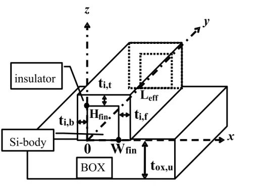
Figure 2-1 shows the schematic sketch of a multi-gate SOI structure. The Si-fin body covered by gate insulator is a cuboid with six faces, and each face is connected to a voltage bias. In the subthreshold regime, the Si-fin body is fully depleted with negligible mobile carriers. Therefore, the potential distribution, φ(x, y, z), satisfies the Poisson’s equation:
(
)
(
)
(
)
si a qN z z y x y z y x x z y x ε φ φ φ =− ∂ ∂ + ∂ ∂ + ∂ ∂ 2 2 2 2 2 2 , , , , , , (2-1)where Na is the doping concentration of the Si-fin. The required boundary conditions can be described as:
(
)
(
)
fg fb W x i si f i fin V V x z y x t z y W fin − = ∂ ∂ ⋅ + = , , , , , φ ε ε φ (2-2a)(
)
(
)
bg fb x i si b i V V x z y x t z y = − ∂ ∂ ⋅ − =0 , , , , , 0 φ ε ε φ (2-2b)(
)
(
)
tg fb H z i si t i fin V V z z y x t H y x fin − = ∂ ∂ ⋅ + = , , , , , φ ε ε φ (2-2c)(
)
(
)
ug fb z ox si u ox z V V z y x t y x = − ∂ ∂ ⋅ − =0 , , , 0 , , φ ε ε φ (2-2d)(
x z)
φms φ ,0, = − (2-2e)(
x Leff z)
=−φms+VDS φ , , (2-2f)where εsi ,εi and εox are dielectric constants of the Si-fin, gate dielectric and oxide, respectively.
Wfin, Hfin, and Leff are defined as fin width, fin height, and channel length, respectively. ti,t, ti,f,
ti,b, and tox,u are thicknesses of top gate dielectric, front gate dielectric, back gate dielectric,
and buried oxide, respectively. Vfg, Vbg, Vtg, Vug and VDS are the voltage biases of front gate,
back gate, top gate, buried gate and drain terminal, respectively. Vfb is the flat-band voltage
for these gate terminals. φms is the built-in potential of the source/drain to the channel.
This 3-D boundary value problem can be divided into three sub-problems, including 1-D Poisson’s equation, 2-D and 3-D Laplace equation. Using the superposition principle, the complete potential solution is φ(x, y, z) = φ1(z) + φ2(x, z) + φ3(x, y, z), where φ1(z), φ2(x, z), and
φ3(x, y, z) are solutions of the 1-D, 2-D, and 3-D sub-problem, respectively. The 1-D solution
9
(
ug fb)
u ox ox si t a V V b= , + − ε ε (2-3c)In solving the 2-D and 3-D sub-problems, approximation was made to avoid the numerical iterations required in finding the eigenvalues [13] and to simplify the solution form. The boundary conditions [Equation (2-2a) to (2-2d)] are simplified by converting the gate dielectric thickness to (εsi /εi) times and replacing the gate dielectric region with an equivalent
Si region [14]. The electric field discontinuity across the gate dielectric and Si-fin interface can thus be eliminated. In other words, the Si-fin body and the gate dielectric region are treated as a homogeneous silicon cuboid with an effective width Weff and an effective height
Heff given by Equation (2-4) and (2-5), respectively.
(
if ib)
i si fin eff W t t W = + , + , ε ε (2-4) u ox t i i si fin eff H t t H = + , + , ε ε (2-5)The 2-D solution φ2(x, z) can be obtained using the method of separation of variables:
( )
∑
∞(
)
= ⎟ ⎟ ⎠ ⎞ ⎜ ⎜ ⎝ ⎛ + ⋅ ⎥ ⎥ ⎦ ⎤ ⎢ ⎢ ⎣ ⎡ ⎟ ⎟ ⎠ ⎞ ⎜ ⎜ ⎝ ⎛ ⎟ ⎟ ⎠ ⎞ ⎜ ⎜ ⎝ ⎛ ⎟⎟ ⎠ ⎞ ⎜⎜ ⎝ ⎛ + − ′ + ⎟ ⎟ ⎠ ⎞ ⎜ ⎜ ⎝ ⎛ ⎟⎟ ⎠ ⎞ ⎜⎜ ⎝ ⎛ + = 1 , , ,2 , sinh sinh sin
i eff oxu b i i si eff eff i b i i si eff i H z t i t x W H i c t x H i c z x π ε ε π ε ε π φ (2-6a) where
(
)
( )
(
)
( )
⎢ ⎢ ⎣ ⎡ ⎟ ⎟ ⎠ ⎞ ⎜ ⎜ ⎝ ⎛ − − + + − − − − ⎟ ⎟ ⎠ ⎞ ⎜ ⎜ ⎝ ⎛ = π π π π i t H i t a i b V V H W i c i u ox eff u ox i fb fg eff eff i 1 2 1 1 2 1 , , sinh( )
(
)
( )
( )
( )
⎥⎥⎦ ⎤ ⎟ ⎟ ⎠ ⎞ ⎜ ⎜ ⎝ ⎛ − − + − − − + 2 2 1 2 2 1 3 1 iπ H iπ t H iπ t ε qN i eff i u ox eff u ox si a , , (2-6b)(
)
( )
(
)
( )
⎢ ⎢ ⎣ ⎡ ⎟ ⎟ ⎠ ⎞ ⎜ ⎜ ⎝ ⎛ − − + + − − − − ⎟ ⎟ ⎠ ⎞ ⎜ ⎜ ⎝ ⎛ = ′ π π π π i t H i t a i b V V H W i c i u ox eff u ox i fb bg eff eff i 1 2 1 1 2 sinh 1 , ,( )
(
)
( )
( )
( )
⎥⎥⎦ ⎤ ⎟ ⎟ ⎠ ⎞ ⎜ ⎜ ⎝ ⎛ − − + − − − + , 2 , 2 1 2 2 1 3 1 iπ H iπ t H iπ t ε qN i eff i u ox eff u ox si a (2-6c)Similarly, the 3-D solution φ3(x, y, z) can also be obtained and expressed as
(
)
[
( )
(
(
)
)
]
(
)
⎟⎟ ⎠ ⎞ ⎜ ⎜ ⎝ ⎛ + ⋅ ⎟ ⎟ ⎠ ⎞ ⎜ ⎜ ⎝ ⎛ ⎟⎟ ⎠ ⎞ ⎜⎜ ⎝ ⎛ + ⋅ − ′ + =∑∑
∞ = ∞ = eff oxu b i i si eff m n eff y n m y n m z t H n t x W m y L k e y k e z y x , , 1 1 , ,3 , , sinh sinh sin sin
π ε ε π φ (2-7a) where 2 2 ⎟ ⎟ ⎠ ⎞ ⎜ ⎜ ⎝ ⎛ + ⎟ ⎟ ⎠ ⎞ ⎜ ⎜ ⎝ ⎛ = eff eff y H n W m k π π (2-7b)
(
)
(
)
( )
( )
(
( )
)
( )
⎟ ⎟ ⎟ ⎟ ⎟ ⎠ ⎞ ⎜ ⎜ ⎜ ⎜ ⎜ ⎝ ⎛ − − + ⎟⎟ ⎠ ⎞ ⎜⎜ ⎝ ⎛ − − ⎟⎟ ⎠ ⎞ ⎜⎜ ⎝ ⎛ − − + ⎪⎩ ⎪ ⎨ ⎧ ⎢ ⎣ ⎡− + − ⋅ − − = 3 2 2 , 2 , , 1 1 2 1 2 1 1 sin 1 π π ε ε ε ε ε π φ m W m t t W qN m b V L k e m eff b i i si m b i i si eff si a m DS ms eff y n m( )
( )
(
)
( )
⎪ ⎪ ⎪ ⎭ ⎪⎪ ⎪ ⎬ ⎫ ⎟ ⎟ ⎠ ⎞ ⎜ ⎜ ⎝ ⎛ + ⎟ ⎟ ⎠ ⎞ ⎜ ⎜ ⎝ ⎛ − ⎟ ⎟ ⎠ ⎞ ⎜ ⎜ ⎝ ⎛ + ⎟ ⎟ ⎠ ⎞ ⎜ ⎜ ⎝ ⎛ − + − − ⋅ ⋅ ⎥ ⎥ ⎥ ⎥ ⎥ ⎦ ⎤ ⎟ ⎟ ⎟ ⎟ ⎟ ⎠ ⎞ ⎜ ⎜ ⎜ ⎜ ⎜ ⎝ ⎛ + − ⎟⎟ ⎠ ⎞ ⎜⎜ ⎝ ⎛ − + ' 2 2 , , 1 sinh 1 2 1 sinh 1 2 1 1 4 1 eff eff eff eff m eff eff eff eff n m n b i i si m b i i si eff W H n m W H m n c W H n m W H m n c n m t t W a π π π π π π ε ε ε ε (2-7c)( )
(
( )
)
⎟⎞ ⎜ ⎛ ⎟⎟ ⎞ ⎜⎜ ⎛ − − ⎟⎟ ⎞ ⎜⎜ ⎛ − 2 2 1 ε ε t t W si m si11 (2-7d)
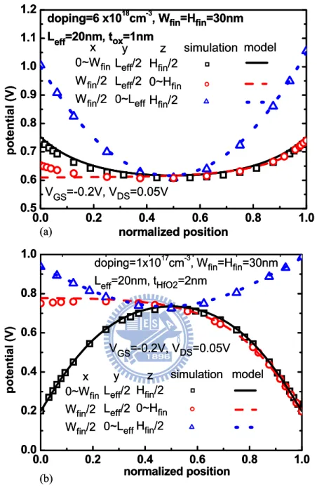
Our potential solution has been verified by 3-D device simulation [15]. Figure 2-2(a) and (b) compare the derived channel potential distribution with device simulation (at VGS = −0.2V)
for heavily doped devices and lightly doped devices, respectively. Note that a smaller EOT is used in the lightly-doped case to sustain the electrostatic integrity [3]. It can be seen that our model shows satisfactory accuracy.
2.2.2 Analytical Channel Potential Solution for GAA Structure
For GAA structure, the cylindrical channel is wrapped by gate insulator and connected to the gate terminal. Since the GAA structure is symmetrical in the θ-direction (Figure 2-3), the 2-D potential distribution φ(r, y) satisfies the 2-D Poisson’s equation:
( )
( )
( )
si a qN y y r r y r r r y r ε φ φ φ =− ∂ ∂ + ∂ ∂ 1 + ∂ ∂ 2 2 2 2 , , , (2-8) The boundary conditions for GAA MOSFETs are( )
=0 ∂ ∂ 0 = r r y r, φ (2-9a)( )
C[
V V(
r D y)
]
r y r fb GS i D r si⋅∂ ∂, = ⋅ − − = 2, 2 = φ φ ε (2-9b)(
)
[
D t D]
Ci =2εi ⋅ln1+2i (2-9c)(
r y)
φms φ , =0 =− (2-9d)(
r y=Leff)
=−φms +VDS φ , (2-9e)Equation (2-9c) is the capacitance per unit length for an infinite long cylindrical capacitor, which neglects the fringing effect of the field near the edges of the capacitor [16].
Similar to the procedure used in the multi-gate structure, this 2-D boundary value problem can be divided into two sub-problems, including 1-D Poisson’s equation and 2-D Laplace equation. Using the superposition principle, the complete potential solution is φ(r, y) = φ1(r) + φ2(r, y), where φ1(r) and φ2(r, y) are solutions of the 1-D and 2-D sub-problems,
respectively. Solving the boundary value problem in cylindrical coordinate [17], the solution can be expressed as
( )
r = Ar2+B 1 φ (2-10a) where si a qN A ε 4 − = (2-10b) ⎟⎟ ⎠ ⎞ ⎜⎜ ⎝ ⎛ + + − = i si si a fb GS C D D qN V V B ε ε 2 2 2 (2-10c)( )
=∑
[
⋅(
⋅)
+ ′ ⋅(
(
−)
)
]
⋅ 0(
⋅)
2 n n eff n n n n y k L y J r k z r λ λ λ φ , sinh sinh (2-11)where Jν(x) is called Bessel function of the first kind of order ν [17]. λn can be determined by
0 = ⎟ ⎠ ⎞ ⎜ ⎝ ⎛ 2 − ⎟ ⎠ ⎞ ⎜ ⎝ ⎛ 2 1 0 J D C D J n n i si n ε λ λ λ (2-12)
13 (2-13a)
(
)
⋅ ⋅ ⎟ ⎠ ⎞ ⎜ ⎝ ⎛ 2 ⋅ ⎥ ⎥ ⎦ ⎤ ⎢ ⎢ ⎣ ⎡ 1 + ⎟⎟ ⎠ ⎞ ⎜⎜ ⎝ ⎛ 2 = ′ 2 0 2 eff n n si n i n L D J C k λ λ ε λ sinh(
)
⎪⎭ ⎪ ⎬ ⎫ ⎪⎩ ⎪ ⎨ ⎧ ⎟ ⎠ ⎞ ⎜ ⎝ ⎛ 2 ⋅ 2 1 − − + ⎥ ⎥ ⎦ ⎤ ⎢ ⎢ ⎣ ⎡ ⎟ ⎠ ⎞ ⎜ ⎝ ⎛ 2 ⋅ ⎟ ⎠ ⎞ ⎜ ⎝ ⎛ 2 ⎟⎟ ⎠ ⎞ ⎜⎜ ⎝ ⎛ 1 2 − ⎟ ⎠ ⎞ ⎜ ⎝ ⎛ 2 ⋅ ⎟ ⎠ ⎞ ⎜ ⎝ ⎛ 2 1 ⋅ − 2 2 1 2 1 3 D J D B D J D D J D A n n ms n n n n λ λ φ λ λ λ λ (2-13b)Figure 2-4 compares the derived channel potential distribution with 3-D device simulation for both lightly doped (1×1015cm-3) and heavily doped (3×1018cm-3) GAA devices.
It can be seen that our model shows satisfactory accuracy for various channel doping.
2.2.3 Modeling of Subthreshold Current and Vth Using the Channel
Potential Solution
The subthreshold current can be derived using the channel potential solution. For example, the current density Jn(r, y) of a GAA device at the position (r, y) can be expressed as
[18]:
( )
( )
( )
( ) ( )
( )
dy y dV q kT y V y r N n q dy y dV y r n q y r J a i n n n ⎥⋅ ⎦ ⎤ ⎢ ⎣ ⎡ − ⋅ − = ⋅ − = , exp , , 2 φ µ µ (2-14)where n(r, y) is the electron density at the position (r, y) and V(y) is the quasi-Fermi potential.
µn is the carrier mobility. The current IDS (y) can be derived by integrating in r and θ
directions:
( )
( ) ( )
( )
dy y dV dr q kT y V y r N n r q y I D a i n DS ⋅ ⎪⎭ ⎪ ⎬ ⎫ ⎪⎩ ⎪ ⎨ ⎧ ⎥ ⎦ ⎤ ⎢ ⎣ ⎡ − ⋅ − − =∫
2 0 2 , exp 2π φ µ (2-15)Since the electron current flow is continuous, the subthreshold current IDS is independent of y
(
)
(
)
[
(
(
)
)
]
( ) (
)
[
]
∫
0∫
0 2 2 ⎥ ⎦ ⎤ ⎢ ⎣ ⎡2 ⋅ − − 1 = eff L D DS a i n DS dr q kT y r r dy q kT V N n q kT q I , exp exp φ π µ (2-16)Since the derivation procedure of IDS for multi-gate structure is similar, the expression of
IDS for multi-gate structure is similar to Equation (2-16) except for the integral term in the
denominator. For multi-gate structure,
(
)
(
)
[
(
(
)
)
]
(
) (
)
[
]
∫
0∫ ∫
0 0 2 ⎥⎦ ⎤ ⎢⎣ ⎡ − − 1 =eff fin fin
L H W DS a i n DS dxdz q kT z y x dy q kT V N n q kT q I , , exp exp φ µ (2-17)
The subthreshold current derived by Equation (2-16) and (2-17) has been verified by 3-D device simulation. Figure 2-5(a) and (b) compares the derived subthreshold current with device simulation for heavily doped devices and lightly doped devices, respectively. Besides, we define the Vth as the gate voltage at which the calculated subthreshold current IDS = 300nA
× Wtotal/Leff [19], where Wtotal is the total width. For multi-gate structure, Wtotal = 2Hfin+Wfin
and for GAA structure, Wtotal = π·D. Since our calculated subthreshold current is applicable
for the subthreshold regime, we focus on the accuracy for VGS below Vth. For heavily doped
devices [Figure 2-5(a)], the Vth is around 0.4V and for lightly doped case [Figure 2-5(b)] the
Vth is around 0.2V. It can be seen that our model shows satisfactory accuracy.
Compared with the TCAD device simulation, our methodology shows higher efficiency in determining the subthreshold current and Vth of multi-gate and GAA devices. In our
calculation, the CPU time needed is less than 20% of that needed for TCAD simulation. More importantly, this theoretical framework provides more scalable and predictive results than
15
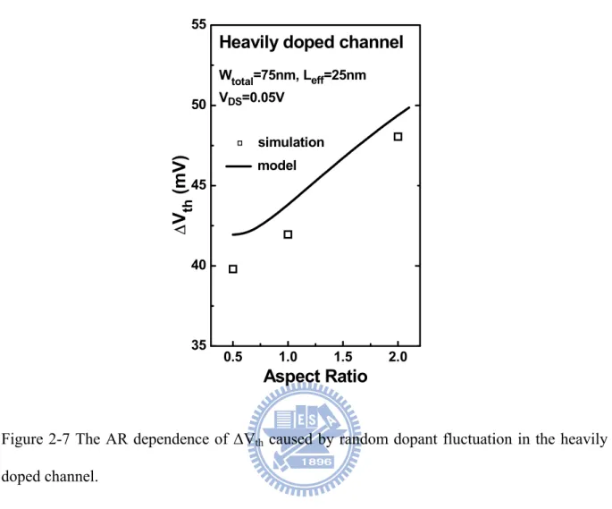
crucial issue to device design. In this section, we compare the Vth dispersion caused by RDF
for FinFET, Tri-gate and Quasi-planar devices with both heavily doped and lightly doped channels [20]. Through our theoretical model, the impact of device aspect ratio on the random dopant fluctuation in multi-gate MOSFETs is examined.
Although the actual 3-D charge distribution is not uniform, we can incorporate the dopant number fluctuation in our theoretical framework to assess the feasibility of various multi-gate device designs. The dopant number in the channel has been found to follow Poisson distribution [21] and the Vth distribution caused by random dopant fluctuation can be
approximated as Gaussian distribution [21]-[23]. With MOSFET scaling, the Vth distribution
gradually changes its shape from the Gaussian to a Poisson-like distribution [23]. To assess the Vth variation of multi-gate devices caused by dopant number fluctuation, we assume that
the dopant number in the channel follows Poisson distribution [23], [24] and the standard deviation (σ) of the dopant number is na1/2, where na is the average dopant number in the
Si-body. The Vth variation for dopant number fluctuation can then be calculated as
∆Vth=|Vth(+3σ)−Vth(−3σ)|/2.
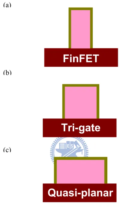
To compare the multi-gate devices with various aspect ratio (AR=Hfin/Wfin), we focus on
the FinFET (AR=2), Tri-gate (AR=1), and Quasi-planar (AR=0.5) structures (Figure 2-6). The total width (Wtotal=2Hfin+Wfin) of various AR devices are all equal to 75nm to make fair
comparison. Besides heavily doped devices, we also examined the impact of RDF on the Vth
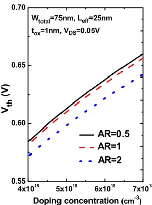
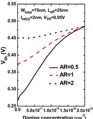
dispersion of lightly doped devices. For heavily doped devices, the channel doping is equal to 6×1018cm-3. For lightly doped channel the channel doping is 1×1017cm-3. Note that gate oxide (tox=1nm) is used for heavily doped devices, while high-k dielectric (tHfO2=2nm and the
dielectric constant of HfO2 is 25) is used for lightly doped ones to sustain the device
electrostatics [3].
with device simulation [15]. For heavily doped channel, the ∆Vth increases with AR, and the
minimum ∆Vth occurs at AR=0.5, i.e., Quasi-planar device. This is because for a given Wtotal,
the devices with AR=0.5 possess the largest channel volume (Figure 2-8). Since
a a th th dN N dV V = ⋅∆ ∆ (2-18) V N V V N V n V n Na = ∆ a ∝ a = a⋅ = a ∆ (2-19)
where V is the channel volume, the devices with larger channel volume show smaller ∆Vth. In
addition to channel volume, Equation (2-18) demonstrates that the Vth sensitivity to the
channel doping (dVth/dNa) may also determine the ∆Vth. Figure 2-9 shows the channel doping
dependence of Vth for devices with heavily doped channel. It can be seen that FinFET,
Tri-gate and Quasi-planar devices show similar Vth sensitivity. Therefore, for heavily doped
channel, Quasi-planar device shows better immunity to RDF than FinFET and Tri-gate because of its larger channel volume.
Figure 2-10 shows that for lightly doped channel, the ∆Vth increases as AR decreases.
This is because for lightly doped channel, devices with different AR show different Vth
sensitivity to channel doping (Figure 2-11). For lightly doped channel, FinFET shows the smallest Vth sensitivity to channel doping because of its narrower Wfin for a given Wtotal. In
other words, Wfin scaling enhances the gate control and reduces the Vth dependence on the
17
calculation. We assume that the 3σ process variations of these device parameters are ±10% of their nominal values, and the Vth variation is defined as ∆Vth=|Vth(+10%)−Vth(−10%)|/2 [24].
The overall Vth variation is defined as ∆Vth2 = ∆Vth,Leff2 + ∆Vth,Wfin2 +∆Vth,Hfin2 + ∆Vth,RDF2.
Figure 2-12(a) shows that for heavily doped channel, random dopant fluctuation dominates the overall Vth dispersion and the Quasi-planar device shows better immunity than devices
with other AR to dopant fluctuation. Our theoretical result is consistent with the experimental data from [25], which showed that for doped channel, the σVth of the devices with smaller
volume is larger than that of the devices with larger volume. Although lightly doped channel has been suggested [26] to suppress the Vth variation caused by dopant fluctuation, Figure
2-12(b) shows that the Vth variation caused by dopant fluctuation is still significant for
lightly-doped Tri-gate and Quasi-planar devices. The impact of RDF may still be an issue to the Vth dispersion of lightly doped channel unless devices with good electrostatic integrity
such as FinFET are used.
2.4 Sensitivity of GAA MOSFETs to Process Variations
− A
Comparison with Multi-Gate MOSFETs
To assess the sensitivity of GAA and multi-gate MOSFETs to process variations, we assume that the device parameters such as Leff, channel diameter (D) of GAA structure, and
Wfin of multi-gate MOSFETs vary by ±2.5nm (±3σ value, σ is the standard deviation) [26].
This 3σ value is estimated from the combination of process variations such as lithography variation, etch variation, and resist trim variation [26]. Similar to the previous section, the impact of dopant number fluctuation is considered assume that the channel dopant number follows the Poisson distribution and the σ of the dopant number is na1/2, where na is the
average dopant number in the Si-channel. The corresponding Vth variation for process
[24].
To compare the GAA structure with multi-gate MOSFETs, the total width (Wtotal) of
GAA (Wtotal = π·D) and multi-gate MOSFETs (Wtotal = 2Hfin + Wfin) are equal to make fair
comparison. Multi-gate structures with various ARs (AR = Hfin /Wfin) are considered,
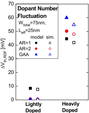
including FinFET (AR = 2) and Tri-gate (AR = 1). Devices with various channel doping are considered. For heavily doped devices, the channel doping is equal to 6×1018cm-3. For lightly doped devices, the channel doping is equal to 1×1017cm-3.
Figure 2-13 shows the calculated ∆Vth caused by dopant number fluctuation (∆Vth,RDF)
for Wtotal = 75nm and Leff = 25nm, and the results are verified with device simulation [15].
The ∆Vth,RDF for heavily-doped GAA device is larger than that of multi-gate MOSFETs. This
is because for a given total width, GAA device possesses smaller channel volume than FinFET and Tri-gate. Besides, it can seen that for heavily doped channel, the ∆Vth,RDF is
significantly larger than that of lightly doped ones. The Vth dispersion due to dopant number
fluctuation is a crucial concern for heavily doped device design.
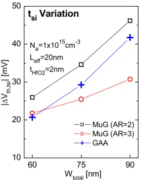
Figure 2-14 shows the calculated ∆Vth caused by Leff variation (∆Vth,Leff) for Wtotal =
75nm and Leff = 25nm. The discrepancies of ∆Vth,Leff for heavily doped devices are not
significant. For lightly doped channel, the ∆Vth,Leff of GAA device is also close to that of
FinFET. However, the ∆Vth,Leff of GAA device is much smaller that that of Tri-gate. The
∆Vth,Leff is determined by the Vth roll-off characteristics. Figure 2-15(a) demonstrates that for