四閘極電晶體具氧化層基體絕緣結構之短通道行為研究
76
0
0
全文
(2)
(3) 四閘極電晶體具氧化層基體絕緣結構之短通道行為研究 指導教授:江德光 博士 國立高雄大學電機工程系 電機工程研究所. 學生:楊鳴傑 國立高雄大學電機工程系 電機工程研究所 摘要. 為了增強電流的驅動能力和改善短通道特性,金氧半場效電晶體元件之發展已從 單閘極傳統平面基材結構(planar SOI single-gate MOSFET)進一步發展具多閘極氧化層 基 體 絕 緣 結 構 (SOI multiple-gate MOSFET) ; 諸 如 雙 閘 極 (Double-gate) 和 三 閘 極 (Triple-gate)電晶體具氧化層基體絕緣結構。近年來具氧化層基體絕緣結構之四閘極電 晶體已引起廣泛的注意與研究,相較於一般的平面電晶體元件,其通道係藉由電晶體 的四個閘極獨立操作加以控制,因此大大的提升數位電路功能應用之靈活性,除此之 外,具氧化層基體絕緣結構之四閘極電晶體尚具有以下電路操作之優點:高直流增益 (high DC gain)、低功率消耗(low power consumption)、低雜訊操作(low noise operation) 與抑制散射效應(immunity of scattering effects),因此四閘極電晶體已成為電路設計的 另一不錯之選擇。 本論文乃基於帕森方程式之全二維解與全三維解,成功地推導出四閘極電晶體具 氧化層基體絕緣結構之短通道行為解析模型,此模型不僅準確顯示出電位分佈 (potential distribution)、短通道臨界電壓縮減(threshold voltage degradation)、汲極偏壓 導致能障降低(drain-induced-barrier-lowering)等效應,而且此模型之演算結果與模擬數 據相當接近,足以提供基本元件設計之導向,並進而被應用於積體電路之模擬。. 關鍵字:多閘極電晶體、短通道行為、汲極偏壓引致通道位能障降低、短通道臨界電 壓縮減 i.
(4) The Investigation on Short-Channel Behavior Model for the SOI Four-Gate Transistor Advisor: Dr. Te-Kuang Chiang Department of Electrical Engineering, Institute of Electrical Engineering, National University of Kaohsiung. Student: MING-JIE YANG Department of Electrical Engineering, Institute of Electrical Engineering, National University of Kaohsiung. ABSTRACT In recent years, silicon-on-insulator (SOI) four-gate transistors have already caused extensive attention. With improved current drive and short-channel characteristics, semiconductors depicts not only switch from bulk to SOI, but also evolve from single-gate planar SOI transistors to multiple-gate devices. Among those novel SOI devices, double- and triple-gate transistors have been demonstrated and modeled. However; the SOI four-gate transistor with low-power and low-noise operation, high intrinsic DC gain, radiation hardness that becomes a promising candidate has not been analytically modeled yet. In this thesis, based on the exact solution of the Poisson equation, we successfully develop an analytical short-channel behavior model for SOI four-gate transistor. Without any fitting parameters, these analytical results are useful in predictive compact modeling of SOI four-gate transistor. The model explicitly shows the distribution of electric potential, short channel threshold voltage roll-off, and drain-induced-barrier-lowing (DIBL) effect. The model is verified by published numerical simulations with close agreement. This model not only gives physical insights into the device physics but also offers the basic designing guidance of the SOI four-gate transistor. Due to its computational efficiency, this model can be applied for SPICE simulation.. Keywords: Multiple-Gate Transistors, Short-Channel Effect, Drain-Induced-Barrier-Lowing, Threshold Voltage roll-off. ii.
(5) Acknowledgements. I am grateful to many people with deep sincerity. This work will not be completed without their support and assistance. First I would like to express my most sincere gratitude to my advisor, Professor Te-Kuang Chiang for his guidance in this work. I would also like to thank many of the past and present members of our research group for their spiritual support and useful discussion.. Finally, I am deeply grateful to my parents for their patience and concern. I could never accomplish the work without their love and advice during these years.. iii.
(6) Contents 摘要. i. Abstract. ii. Acknowledgements. iii. Contents. iv. List of Figures. vi. Chapter 1 Introduction. 1. 1.1. Device Overview. 1. 1.2. Device Structure and Operation. 3. 1.3. Scope and Brief Description of the Thesis. 7. Chapter 2 Two Dimensional Model for SOI Four-Gate Transistor 2.1. Model Derivation. 2.2. 2-D Boundary Conditions Value Problem. 8 8 10. 2.3 1-D Solution. 13. 2.4 Scaling Length. 14. 2.5 Coefficients Solution. 16. 2.6 2-D Generalized Potential Model. 18. 2.7. Potential Contour. 22. 2.8. Maximum Surface Potential. 24. 2.9. Threshold Voltage Related to Front Gate. 26. 2.10. Results and Discussion. 31. Chapter 3 Three Dimensional Model for SOI Four-Gate Transistor. 32. 3.1. Model Derivation. 32. 3.2. 3-D Boundary Conditions Value Problem. 34. 3.3 1-D and 2-D Solution. 36. 3.4. 37. 3-D Laplace Equation Solution. 3.5 Coefficients Solution. 39. 3.6 3-D Generalized Potential Model. 42. 3.7. Potential Contour. 50. 3.8. Minimum Surface Potential. 52. 3.9. Short-Channel Behavior of the SOI G4-FET. 55. iv.
(7) 3.10. Results and Discussion. 60. Chapter 4 Conclusions and Future Works. 61. 4.1. Conclusions. 61. 4.2. Future Works. 61. References. 62. v.
(8) List of Figures Fig.1.1 G4-FET voltage-controlled negative resistance device: (a) G4-NOR schematic, (b) Current voltage characteristics (V= VP)……………...………………………...….………...2 Fig.1.2 Structure of the n-channel G4-FET..............................................................................3 Fig.1.3 Cross-section view related to the MOSFET operation mode of the G4-FET..............4 Fig.1.4 The cross-section view and the direction of current simulated by 3-D simulation at MOSFET operation mode........................................................................................................4 Fig.1.5 Cross-section view related to the DAA mode of the G4-FET: (a) both interface depleted, (b) front interface inverted, back interface depleted, (c) both interface inverted……………………………………………………………………………………....5 Fig.1.6 The cross-section view and the direction of current simulated by 3-D simulation at DAA operation mode………………………………………………………………………...6 Fig.2.1 The cross-section view of n-channel G4-FET………………………………………..8 Fig.2.2 The simulated potential variation with y-direction at x=W/2, VG2=0V, and VG2=3V and the effective substrate bias of VGeff2 is also included for comparison.…………………..12 Fig.2.3 The contour plot of the electrostatic scaling length versus insulator thickness and silicon thickness for the SOI G4-FET………………………………………………………15 Fig.2.4 The decay of Fourier series Cn, Pn, and Qn coefficients versus the term number......17 Fig.2.5 The 3-D potential distribution from the device simulator of ISE for symmetrical junction-gate device of VJG1= VJG2=0V………………………………………………….....19 Fig.2.6 The 3-D potential distribution from the model results for symmetrical junction-gate device of VJG1= VJG2=0V…………………………………………………………………...19 Fig.2.7 The 3-D potential distribution from the device simulator of ISE for asymmetrical junction-gate device of VJG1= 0V and VJG2=-1V…………………………………...............20 Fig.2.8 The 3-D potential distribution from the model results for asymmetrical junction-gate device of VJG1= 0V and VJG2=-1V..........................................................................................20 Fig.2.9 The variation of the surface potential of ψ(x,y=0) and ψ(x,y=tsi) with the normalized channel width position of x/W for the different junction-gate biases of VJG2=-1V and vi.
(9) VJG2=0V and the effective substrate bias of VGeff2 is also included for comparison...............21 Fig.2.10 The variation of the channel potential ψ(x,y) with the normalized channel height position of y/tsi for the different channel locations of x=10nm, x=20nm, and x=40nm and the effective substrate bias of VGeff2 is also included for comparison.....................................21 Fig.2.11 The analytical potential contours with channel width of W=60nm (defined as solid line) as well as those simulated by the two-dimensional device simulator (defined as symbol)..................................................................................................................................22 Fig.2.12 The analytical potential contours with channel width of W=80nm (defined as solid line) as well as those simulated by the two-dimensional device simulator (defined as symbol)..................................................................................................................................23 Fig.2.13 The analytical potential contours with channel width of W=120nm (defined as solid line) as well as those simulated by the two-dimensional device simulator (defined as symbol)..................................................................................................................................23 Fig.2.14 The maximum front surface potential on the back-gate bias of VG2 bias for different channel thickness....................................................................................................25 Fig.2.15 The maximum front surface potential on the back-gate bias of VG2 bias for different channel width..........................................................................................................25 Fig.2.16 The variation of the threshold voltage related to the front gate with the back-gate bias for the different junction gate biases..............................................................................28 Fig.2.17 The variation of the threshold voltage related to the front gate with the channel thickness of tsi .......................................................................................................................29 Fig.2.18 The dependence of the threshold voltage related to the front gate on the back-gate bias with the channel width as a parameter...........................................................................30 Fig.3.1 The structure of n-channel G4-FET………………………………………………...32 Fig.3.2 The simulated potential variation of ψ(x=W/2,y,z=L/2) with VGS2=0V and VGS2=3V and the effective substrate bias of VGeff2 is also included for comparison…………………..35 Fig.3.3 The decay of Fourier series Rmn coefficients versus the term number. ……………41 Fig.3.4 The 3-D potential distribution from the device simulator of ISE for symmetrical junction-gate device VJG1= VJG2=0V at zmin………………………………………………..44 vii.
(10) Fig.3.5 The 3-D potential distribution from model results for symmetrical junction-gate device VJG1= VJG2=0V at zmin………………………………………………………………44 Fig.3.6 The 3-D potential distribution from the device simulator of ISE for asymmetrical junction-gate device VJG1= 0V, VJG2=-1V at zmin…………………......…………………….45 Fig.3.7 The 3-D potential distribution from model results for asymmetrical junction-gate device VJG1= 0V, VJG2=-1V at zmin………………………………………………………….45 Fig.3.8 The 3-D potential distribution at top gate surface from the device simulator of ISE for VDS= 0V............................................................................................................................46 Fig.3.9 The 3-D potential distribution at top gate surface from model results for VDS= 0V...........................................................................................................................................46 Fig.3.10 The 3-D potential distribution at top gate surface from the device simulator of ISE for VDS= 0.5V.........................................................................................................................47 Fig.3.11 The 3-D potential distribution at top gate surface from model results for VDS= 0.5V.…………………………………………………………………………………….......47 Fig.3.12 The variation of the surface potential of ψ(x,y=0,zmin) and ψ(x,y=tsi,zmin) with the normalized channel width position x/W for the different junction-gate biases of VJG2=-1.0V and VJG2=0.0V and the effective substrate bias of VGSeff2 is also included for comparison….48 Fig.3.13 The variation of the channel potential of ψ(x,y,zmin) with the normalized channel height position y/tsi for the different channel locations of x=10nm, x=20nm and x=40nm and the effective substrate bias of VGSeff2 is also included for comparison……………………….48 Fig.3.14 The variation of the surface potential of ψ(xmax,y=0,z) and ψ(xmax,y=tsi,z) with the normalized channel length position z/L for the different drain biases of VDS=0V and VDS=0.5V and the effective substrate bias of VGSeff2 is also included for comparison…….....49 Fig.3.15 The variation of the channel potential of ψ(xmax,y,z) with the normalized channel height position y/tsi for the different channel locations of z=30nm, z=60nm and z=120nm and the effective substrate bias of VGSeff2 is also included for comparison…………………..49 Fig.3.16 The analytical potential contours of ψ(x,y,zmin) (defined as solid line) as well as those simulated by there-dimensional device simulator (defined as dash line).....................50 viii.
(11) Fig.3.17 The analytical potential contours of ψ(xmax,y,z) (defined as solid line) as well as those simulated by there-dimensional device simulator (defined as dash line).………........51 Fig.3.18 The potential contours of ψ(xmax,y,z) by 3-D device simulator with VDS=0.5V….51 Fig.3.19 The analytical potential contours of ψ(x,y=0,z) (defined as solid line) as well as those simulated by there-dimensional device simulator (defined as dash line).....................52 Fig.3.20 The minimum front surface potential of ψ 1,min related to the junction gate bias with the channel width as a parameter and the effective substrate bias of VGSeff2 is also included for comparison……………………………………………………………………54 Fig.3.21 The minimum front surface potential of ψ 1,min related to the channel length with the channel width as a parameter……………………………………………………...........54 Fig.3.22 The threshold voltage roll-off related to the channel length with the thickness of silicon film as a parameter.....................................................................................................57 Fig.3.23 The threshold voltage roll-off related to the channel length with the thickness of front gate oxide as a parameter. ………………................………………......……………..58 Fig.3.24 The threshold voltage roll-off related to the channel length with the channel width as a parameter. ......................................................................................................................58 Fig.3.25 The threshold voltage roll-off related to the channel length with the junction-gate bias as a parameter.................................................................................................................59. ix.
(12) Chapter 1 INTRODUCTION 1.1 Device Overview The International Technology Roadmap for Semiconductors portrays that semiconductors not only switch from bulk to silicon-on-insulator (SOI)[2], but also develop from single-gate planar SOI transistors to multiple-gate devices to enhance current drive and improve short-channel characteristics. Among those novel SOI devices, double- and triple-gate transistors have been demonstrated and modeled. The SOI four-gate transistor is an innovative device first proposed by Blalock et al [1]. It comprises a channel surrounded by four gates with independent biases. This device is basically consists of MOSFET and JFET in the same device. Besides, it is based on the standard partially or fully depleted (FD) SOI processes, without necessitating additional fabrication steps. The advantages provided by four independent gates are discussed by discriminating different operation mode: volume and surface conduction. Due to its maximum functional flexibility[2], high intrinsic DC gain[3], low-power and low-noise operation[4], and radiation hardness[5], the G4-FET offers exciting option to circuit designers. The conduction parameters (i.e. threshold voltage, transconductance, subthreshold slope, etc.) related to the input gate for the G4-FET may be adjusted and optimized by the biases on the remaining gates. Such a technique was used in [6] to build a temperature-compensated voltage reference. Furthermore, the G4-FET provided the opportunity to build multiple-input circuits with dramatically reduced the number of transistors in the proposed circuit, compared to conventional single-gate MOSFET based multipliers. It suggests that only four G4-FET and a current source are required for analog multiplier[7]. In addition, only one G4-FET and a load device can also be used to build a digital non-majority voting circuit[8]. The voltage controlled negative resistance device (G4-NOR) for another example is shown in Fig. 1.1 [9]. The G4-NOR requires only two G4-FET s that are connected as a lambda diode (Fig. 1(a))[10]. The additional MOS gates of the G4-FET s are used to modulate the peak current and the valley voltage, via voltages VN and VP. 1.
(13) (a). (b). 4. Fig. 1.1 G -FET voltage-controlled negative resistance device: (a) G4-NOR schematic, (b) Current voltage characteristics (V= VP)[11]. Further exploitation and use of the G4-FET in circuits require physics-based transistor model. Gentil et al[12] have used the quasi-2D parabolic potential approximation to build the model of the channel potential and threshold voltage for the device. However, due to drawback of quasi-2D parabolic approach, it can not precisely predict the complete two-dimensional potential distribution, which is essential to illustrate gate-coupling mechanism regarding how the electric fields between the gates for the vertical SOI MOSFET and lateral JFET are coupled. To entirely control the device operation in the circuit application, there is a need to develop the potential distribution and the threshold voltage model, which are important for establishing the static current-voltage characteristic. In this thesis, we successfully developed a analytical model for the short-channel potential distribution and threshold voltage of a SOI G4-FET based on the exact solution of Poisson equation, which is solved by the superposition method[13]. The simulation data calculated by the analytical model makes a close agreement with those simulated by the device simulator[14] over a wide range of the device parameters. This model not only gives physical insights into the device physics but also offers the basic designing guidance of the SOI Four-gate transistor.. 2.
(14) 1.2 Device Structure and Operation The G4-FET’s structure is shown in Fig. 1.2 It’s defined as an n-channel accumulation-mode SOI MOSFET provided with two lateral junction-gate ( VJG1 and VJG2 ) exercising an extra JFET control on the channel. The G4-FET has four gates independently biased: a poly-silicon top gate VG1, a substrate emulating a back gate VG2, and two junction gates VJG1 and VJG2.. Fig. 1.2. Structure of the n-channel G4-FET.. The combined MOS and JFET effects in the G4-FET are used to modulate the three possible current components: front surface accumulation current (mainly controlled by the front gate), the back surface accumulation current (mainly controlled by the back gate) and the volume current whose cross-section dimensions are controlled by the all gates [15]. The role of the poly-silicon top gate VG1 depends on the operation mode. It could induce accumulation at the front interface leading to surface conduction, and induce depletion or inversion when the G4-FET operates in volume conduction mode. The back gate VG2 acts similarly as VG1. The lateral junction are reverse biased by VJG1 and VJG2 to provide a JFET-like control. The operation of the G4-FET can be listed as follows [11]:. 3.
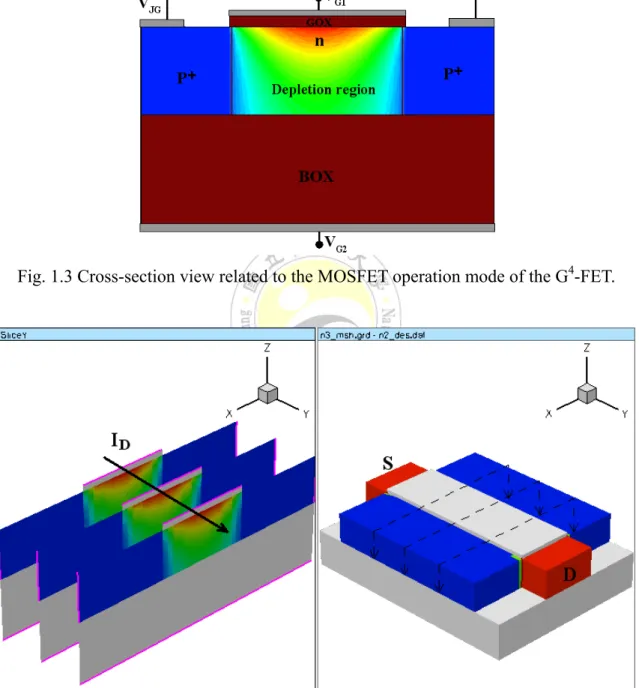
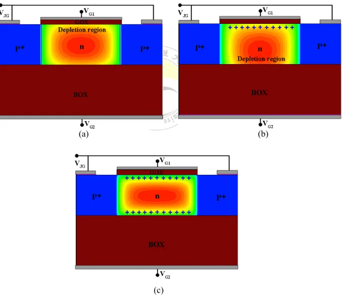
(15) (i). MOSFET modes: The G4-FET is driven by VG1 while VG2 and VJG are biased to a constant voltage and fully deplete the body. In Fig. 1.3 illustrates the cross-section of G4-FET channel for MOSFET mode. Fig.1.4 shows the cross-section and the direction of current used 3-D simulation that operates at MOSFET mode. Drain current consists of a front accumulation current.. Fig. 1.3 Cross-section view related to the MOSFET operation mode of the G4-FET.. Fig. 1.4 The cross-section view and the direction of current simulated by 3-D simulation at MOSFET operation mode.. 4.
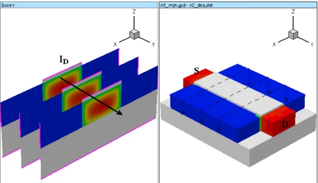
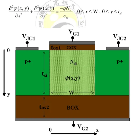
(16) (ii). Depletion-All-Around (DAA) mode: DAA consists of a volume channel surrounded by depletion regions induced by VJG are reverse-biased, while the VG1 and VG2 induced depletion or inversion so that the G4-FET drain current only depends on the volume charge flowing in the center of the film. There are three possible combinations of the DAA conduction[15]: both interfaces depleted in Fig. 1.5(a), one interface depleted while the other is in inversion in Fig. 1.5(b), and both interfaces VG1 and VG2 in inversion in Fig. 1.5(c). Note that the cross-section dimensions of DAA conducting channel can be extremely reduced, leading to a quantum wire[2]. Fig. 1.6 shows the cross-section and the direction of current used 3-D simulation that operates at DAA mode.. (a). (b). (c) Fig. 1.5 Cross-section view related to the DAA mode of the G4-FET: (a) both interface depleted, (b) front interface inverted, back interface depleted, (c) both interface inverted. 5.
(17) Fig. 1.6 The cross-section view and the direction of current simulated by 3-D simulation at DAA operation mode. Recently, Akarvardar et al[15] analyzed these various operation modes of the G4-FET based on the measured current-voltage, transconductance and threshold characteristics. They used numerical simulations to clarify the role of volume or interface conduction mechanisms and illustrated excellent performance of subthreshold swing[16] and tansconductance for the device. On the basic measured drain current and transconductance, Akarvardar et al[17] analyzed the G4-FET’s low-frequency noise characteristic by discriminating two different operation modes such as accumulation mode and JFET mode(the same operation of DAA). They reported that the volume of the transistor generated less noise than its surface. In DAA mode, the device has the excellent analog performance due to the majority carriers to flow in the volume of the silicon film far from the silicon and oxide interface. The influence of the oxide and interface defects on traditional MOS transistor is very sensitive for low-noise and radiation-hard application[18-20]. The defects can seize and discharge the conducting channel carriers and generate noise. If the defects concentration increases during operation as a consequence of exposure to ionizing radiation, they give rise to a change in device parameters, i.e., threshold voltage shift, subthreshld swing and transconductance degradation[3]. As the interface defects can be effaced in DAA mode, the noise performance and the radiation hardness are expected to 6.
(18) improve. Akarvardar et al has demonstrated that in DAA mode, the control of the junction gates on the volume channel is most efficient when both interface are biased in inversion by applying appropriate voltage to VG1 and VG2 [11]. When the interface is in strong inversion, the minority carriers (holes) protect the interface so that the radiation-hardness oxide/interface charges can not modulate the surface potential and the vertical depletion widths [11].. 1.3 Scope and Brief Description of the Thesis In this thesis, the G 4 -FET will focus on surface conduction that used like an accumulation-mode MOSFET, it is driven by the front gate VG1. The potential distribution and the surface threshold voltage are modeled in chapter 2 and chapter 3. The chapter 2 will show the 2-D analytical modeling for the G4-FET to discuss gates coupling mechanism and the VG1 surface threshold voltage with variable VG2 basis of accumulation, depletion and inversion regions. Since the 2-D model can not really describe the practical drain current flow, the chapter 3 will show the 3-D analytical model and extends to the short-channel effect and drain-induced barrier-lowing effects. The 2-D and 3-D analytical model are verified with wide rang of device parameters on simulation results. Finally, chapter 4 will make a short conclusion and proposes future works.. 7.
(19) Chapter 2 TWO DIMENSIONAL MODEL FOR SOI FOUR-GATE TRANSISTER 2.1 Model Derivation The n-channel G4-FET cross-section is shown in Fig. 2.1, the symbols and axes used for modeling are also indicated in this figure. We assume that the impurity density is uniform in the channel region. The channel potential distribution is expressed by. ψ ( x, y ) . We assume that the channel region is fully-depleted. According to the Poisson equation, the channel potential distribution can be written as eq.(2.1) [21]. ∂ 2ψ ( x, y ) ∂ 2ψ ( x, y ) −qN d + = ∂x 2 ∂y 2 ε si. 0 ≤ x ≤ W , 0 ≤ y ≤ tsi. Fig. 2.1 The cross-section view of n-channel G4-FET.. 8. (2.1).
(20) Where Nd is the uniform doping concentration of the silicon film, tox1 is the gate oxide thickness, tox2 is the buried oxide thickness, tsi is the silicon film thickness, W is the device channel width, and the y-axis is perpendicular and the x-axis is parallel to the channel width, respectively. By using the superposition method, the resultant solution. ψ ( x, y ) can be composed with one-dimensional (1-D) potential solution V(y) and 2-D potential solution U(x,y) which satisfy the following 2-D Laplace equation and 1-D Poisson equation, respectively[13].. ψ ( x, y ) = V ( y ) + U ( x, y ). (2.2). Substituting eq.(2.2) into eq.(2.1), we obtain. ∂ 2U ( x, y ) ∂ 2V ( y ) ∂ 2U ( x, y ) −qN d + + = ∂x 2 ∂y 2 ∂y 2 ε si. (2.3). 1-D Poisson equation ∂ 2V ( y ) − qN d = ∂y 2 ε si. (2.4). ∂ 2U ( x, y ) ∂ 2U ( x, y ) + =0 ∂x 2 ∂y 2. (2.5). 2-D Laplace equation. 9.
(21) 2.2 2-D Boundary Conditions Value Problem The Poisson equation is solved by using the following boundary conditions: (A) At the top side, electric flux at the interface of silicon/gate oxide is continuous: ∂ψ (x, y ) ∂y. y =0. =−. ε ox VG1 − VFB1 −ψ (x, y ) × tox1 ε si. (0 ≤ x ≤ W). (2.6). Where VG1 is the top gate bias, tox1 is the gate oxide thickness, εsi is permittivity of silicon(εsi =11.7×8.85×10-14 ), εox is permittivity of oxide(εox =3.9×8.85×10-14), and VFB1 is the flat-band voltage of front bias given as the difference between front gate material work function and silicon work function.. VFB1 = φM ,top − φsi. (2.7). φsi is the silicon work function, which is given by φsi = χsi +. Eg 2q. − φB. (2.8). Where Eg is the silicon bandgap at 300 K, χsi is the electron affinity of silicon, φB is the Fermi potential (= VT × ln( N d ni ) ), VT is the thermal voltage(=kT/q), and ni is the intrinsic carrier concentration. (B) At the bottom side, electric flux at the interface of silicon/buried oxide is continuous. ∂ψ (x, y ) ∂y. y =tsi. =. ε ox VG2 − VFB 2 −ψ (x, y ) × tox2 ε si. (0 ≤ x ≤ W). (2.9). Where VG2 is the bottom gate bias, VFB2 is the flat-band voltage of back gate, tox2 is the back oxide thickness. VFB2 = φM ,bottom − φsi. (2.10). (C) The potential at the VJG1 end is. ψ (0, y ) = VJG1 -φb Where φb. (0 ≤ y ≤ t si ). (2.11). is the potential barrier between the junction-gates and the. channel(=Eg/2+VTln(Nd/ni) [12]. 10.
(22) (D) The potential at the VJG2 end is. ψ (W, y ) = VJG2 -φb. (0 ≤ y ≤ t si ). (2.12). Note that (A) and (B) imply that a linear variation of potential goes inside the oxide and both of them is only valid for the very thin gate oxide. For the thick buried oxide, we need to use the effective back-gate bias to compensate the non-linearity of the potential distribution in the buried gate oxide[22]. Fig. 2.2 shows the simulated potential variation with y-direction at x=W/2, VG2=0V, and VG2=3V and the effective substrate bias of VGeff2 is also included for comparison. The potential does not vary linearly inside the buried oxide at VG2=0V due to the influence of the junction gates electric fields. But when VG2>0, the variation of potential with the back-gate bias will gradually become linear, it is because the back-gate bias effect alleviate the junction gates electric fields or even be predominant. To account for this nonlinearity, we use a modified boundary condition, where an effective back-gate voltage VGeff2 [22] is introduced.. ∂ψ (x, y ) ∂y. y = tsi. =. ε ox VGeff2 − VFB 2 −ψ (x, y ) × tox2 ε si. (0 ≤ x ≤ W). (2.13). VGeff2 is defined by V Geff2 = VG 2 +ψ (W / 2, y ) + tox 2 × (. 11. ∂ψ (W / 2, y ) ) ∂y. y =tox1 + tsi. (2.14).
(23) 0. GOX Dash line : Model with effective substrate bias Solid line: ISE. Device Height, y (nm). 10 20. Silicon film. 30. Na = 1< 1020 cm-3. 40. Nd=1< 1017cm-3. 50. tox1 = 5 nm tox2 = 50 nm tsi = 40 nm W=80 nm VG1 = 0 V VJG = 0 V. BOX. 60 70 80 90 -1. VG2=0V. VG2=1V. VG2=2V. VG2=3V. 0 1 2 Potential, Y(x=W/2,y) (V). Fig. 2.2 The simulated potential variation with y-direction at x=W/2, VG2=0V, and VG2=3V and the effective substrate bias of VGeff2 is also included for comparison.. 12. 3.
(24) 2.3 1-D Solution From boundary condition (A) and (B), we get ∂V ( y ) ∂y. ∂V ( y ) ∂y. =− y =0. = y = tsi. ε ox VG1 − VFB1 − V ( y ) × ε si tox1. (2.15). ε ox VG2 − VFB 2 − V ( y ) × ε si tox2. (2.16). Using eq.(2.15) and eq.(2.16), 1-D solution can be obtained as V ( y) = −. qN d 2 y + ay + b 2ε si. (2.17). Where a=. b=. 2 (VFB1 − VFB 2 − VG1 + VG 2 ) ε oxε si +qN Dtsi ( tsiε ox + 2tox 2ε si ). (2.18). 2ε si ( tsiε ox + ε si ( tox1 + tox 2 ) ). {. }. 2ε ox tsiε ox (VG1 − VFB1 ) − ε si ⎡⎣tox 2 (VFB1 − VG1 ) + tox1 (VFB 2 − VG 2 ) ⎤⎦ +qN D tsi tox ( tsiε ox + 2tox 2ε si ) 2ε ox ( tsiε ox + ε si ( tox1 + tox 2 ) ). (2.19). 13.
(25) 2.4 Scaling Length By using separation method together with boundary condition, one obtains the following resultant solution of the two-dimensional Laplace equation. From eq.(2.5) and by letting U ( x, y ) = X ( x)Y ( y ). (2.20). By substituting eq.(2.20) into eq.(2.5), we obtain X '' ( x)Y ( y ) + X ( x)Y '' ( y ) = 0. (2.21). eq.(2.21) divided by X ( x)Y ( y ) , one obtains X '' ( x) Y '' ( y ) + =0 X ( x) Y ( y ). (2.22). X '' ( x) Y '' ( y ) =− = k2 X ( x) Y ( y). (2.23). X ( x) = a1e − kx + a2 ekx. (2.24). By letting. We obtain. Y( y ) = a3cos (ky ) + a4 sin(ky ). (2.25). Due to a3cos (ky ) + a4 sin(ky ) = a32 + a42 sin ( ky + θ ) , eq.(2.20) can be rewritten as ∞. (. ). U ( x, y ) = ∑ a32 + a4 2 a1e − kn x + a2 ekn x sin ( kn y + θ n ) n =1. (2.26). Let a32 + a42 × a1 = Pn ,. a32 + a42 × a2 = Qn. (2.27). and we obtain ∞. (. ). U ( x, y ) = ∑ Pn e − kn x + Qn e kn x sin ( kn y + θ n ) n =1. (2.28). Where kn (k=π/λ)is the eigenvalue equation for the scale length, θ n is triangular parameters. 14.
(26) From boundary condition (A) and (B), one obtain ∂U ( x, y ) ∂y. ∂U ( x, y ) ∂y. =. ε ox U ( x, y ) × ε si tox1. (2.29). =. ε ox −U ( x, y ) × tox2 ε si. (2.30). y =0. y = tsi. From eq.(2.29) and (2.30), we obtain tan kntsi = tan θ n =. ε oxε si kn ( tox1 + tox 2 ) ε si 2 kn 2tox1tox 2 − ε ox 2. (2.31). ε si tox1kn ε ox. (2.32). Fig. 2.3 shows the contour plot of the electrostatic scaling length versus insulator thickness and silicon thickness for the SOI G4-FET. It is obviously seen that both thin insulator and silicon film will be required for the small scaling length which decreases the 2D effects causing DIBL and threshold voltage degradation.. Insulator Thickness, tox1 (nm). 10. λ=70nm. 8. λ=60nm 6. λ=50nm λ=40nm λ=30nm λ=20nm. 4. λ=10nm 2 0. 5. 10 15 Silicon Thickness, tsi (nm). 20. 25. Fig. 2.3 The contour plot of the electrostatic scaling length versus insulator thickness and silicon thickness for the SOI G4-FET. 15.
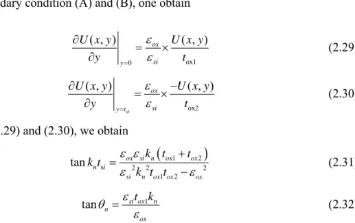
(27) 2.5 Coefficients Solution The Fourier series coefficients of Pn, Qn, Cn and Dn in the resultant solution of the two-dimensional Laplace equation can are expressed as Pn = Qn =. Cn e KnW − Dn 2sinh( K nW ). (2.33). −Cn e− KnW + Dn 2sinh( K nW ). (2.34). with Cn = Dn =. 2 × q × ND. × γ − 4 × a ×η + 4 × (VJG1 − φb − b ) × ρ. (2.35). 2 × q × ND. × γ − 4 × a ×η + 4 × (VJG 2 − φb − b ) × ρ. (2.36). ε si. ε si. Where γ, η and ρ in above equations are defined as. γ=. cos ( kntsi + θ n ) ( 2 − kn 2 × t si 2 ) − 2 cos θ n + 2tsi kn sin ( kntsi + θ n ) 2tsi kn 3 − kn 2 sin ( 2 ( kntsi + θ n ) ) + kn 2 sin 2θ n. ⎡sin ( kntsi + θ n ) − sin θ n − kntsi cos ( kn tsi + θ n ) ⎤⎦ η=⎣ 2tsi kn 2 − kn sin ( 2 ( kn tsi + θ n ) ) + kn sin 2θ n. ρ=. cos θ n − cos ( kn tsi + θ n ). 2tsi kn − sin ( 2 ( kn tsi + θ n ) ) + sin 2θ n. (2.37). (2.38). (2.39). Fig. 2.4 shows the decay of Fourier series Pn, Qn and Cn coefficients versus the term number. Since the Fourier series coefficients decay rapidly, the first term of Pn, Qn, and Cn will dominate the whole series and be used to derive the threshold voltage according to the minimum surface potential[23].. 16.
(28) Coefficient (Pn,Qn,Cn,). 0.4 0 -0.4 ’ : Qn # : Pn & : Cn. -0.8 -1.2. tox1 = 5 nm tox2 = 50 nm tsi = 40 nm VG1 = 0 V VG2 = 0V VJG = 0 V. Vfb1=Vfb2=0 V Na = 1< 1020 cm-3 Nd=1< 1017cm-3 W=80 nm. -1.6 0. 4. 8 Term Number, n. 12. 16. Fig. 2.4 The decay of Fourier series Cn, Pn, and Qn coefficients versus the term number.. 17.
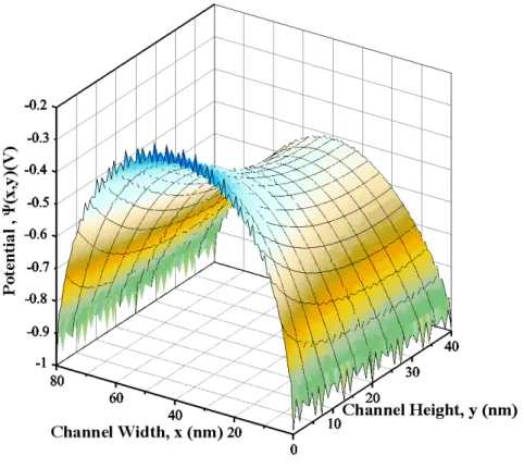
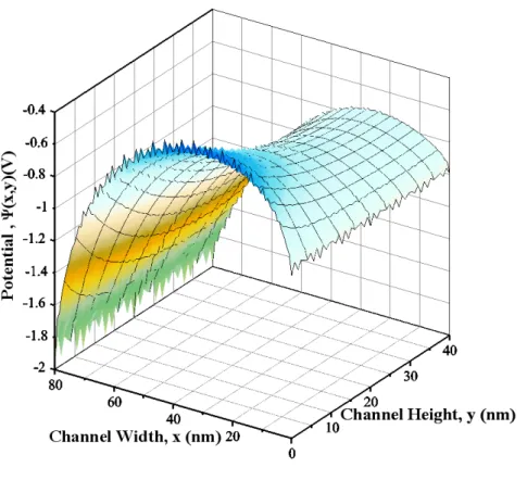
(29) 2.6 2-D Generalized Potential Model The full expression for the potential in silicon channel region is. ψ ( x, y ) = −. ∞ qN d 2 y + ay + b + ∑ Pn e − kn x + Qn ekn x sin ( kn y + θ n ) 2ε si n =1. (. ). (2.40). To verify the analytical body potential model, Fig. 2.5 and Fig. 2.6 show the 3-D potential distribution from the device simulator of ISE[14] and model results with the same device structure and bias condition for symmetrical junction-gate device with VJG1= VJG2=0V. Fig. 2.7 and Fig. 2.8 show the device simulator and model results for asymmetrical VJG1=0V, VJG2=-1V, respectively. It is obviously seen that a close agreement for the 3-D potential distribution between the device simulator and analytical model are obtained. Fig. 2.9 shows the variation of the surface potential ψ(x,y=0) and ψ(x,y=tsi) with the normalized channel width position x/W for the different junction-gate biases of VJG2=-1V and VJG2=0V and the effective substrate bias of VGeff2 is also included for comparison.. A good agreement between the results calculated from our model with those simulated using the device simulator is obtained. It is observed that when the junction-gate bias of VJG2 is decreased from 0V to -1V, the maximum potential for both surface at y=0 and y=tsi are decreased. The reduced maximum surface potential will make it more difficult for the majority carrier to accumulate near the surface and will pull up the threshold voltage. Fig. 2.10 shows the variation of the channel potential ψ(x,y) with the normalized channel height position y/tsi for the different channel locations of x=10nm, x=20nm, and x=40nm and the effective substrate bias of VGeff2 is also included for comparison. It can be seen that at the middle of the channel of x=40nm, the surface potential of ψ(x,y=0) and ψ(x,y=tsi) is much larger than that for the location of x=10nm and x=20nm. It implies that the device turn-on point will easily occurs at the middle of the surface due to easier accumulation operation for the larger surface potential happening at x=40nm=W/2 which corresponds to the equation of xmax= W/2=ln(P1/Q1)/2k1.. 18.
(30) Fig. 2.5 The 3-D potential distribution from the device simulator of ISE for symmetrical junction-gate device of VJG1= VJG2=0V.. Fig. 2.6 The 3-D potential distribution from the model results for symmetrical junction-gate device of VJG1= VJG2=0V. 19.
(31) Fig. 2.7 The 3-D potential distribution from the device simulator of ISE for asymmetrical junction-gate device of VJG1= 0V and VJG2=-1V.. Fig. 2.8 The 3-D potential distribution from the model results for asymmetrical junction-gate device of VJG1= 0V and VJG2=-1V. 20.
(32) 0. Potential, Y (x,y)(V). y=0. -0.4 -0.8 y=tsi tox1 = 5 nm tox2 = 50 nm tsi = 40 nm VG1 = 0 V VG2 = 0V VJG1 = 0 V. -1.2 -1.6. Vfb1=Vfb2=0 V Na= 1< 1020 cm-3 # : VJG2=0V & : VJG2=-1V Nd=1< 1017cm-3 W=80 nm Symbol : ISE Solid line : Model Dash line : Model with effective substrate bias. -2 0. 0.2. 0.4. 0.6. 0.8. 1. Normalized Channel Width Position , (x/W) Fig. 2.9 The variation of the surface potential of ψ(x,y=0) and ψ(x,y=tsi) with the normalized channel width position of x/W for the different junction-gate biases of VJG2=-1V and VJG2=0V and the effective substrate bias of VGeff2 is also included for comparison. # : x=40nm Vfb1=Vfb2=0 &: x=20nm Na = 1< 1020 cm-3 +: x=10nm N =1< 1017cm-3 d W=80 nm tsi = 40 nm. Potential, Y(x,y) (V). -0.2. -0.4. tox1 = 5 nm tox2 = 50 nm VG1 = 0 V VG2 = 0V VJG1 = 0 V VJG2 = 0 V. -0.6 Symbol : ISE Solid line : Model Dash line : Model with effective substrate bias. -0.8 0. 0.2. 0.4. 0.6. 0.8. 1. Normalized Channel Height Position , (y/tsi) Fig. 2.10 The variation of the channel potential ψ(x,y) with the normalized channel height position of y/tsi for the different channel locations of x=10nm, x=20nm, and x=40nm and the effective substrate bias of VGeff2 is also included for comparison. 21.
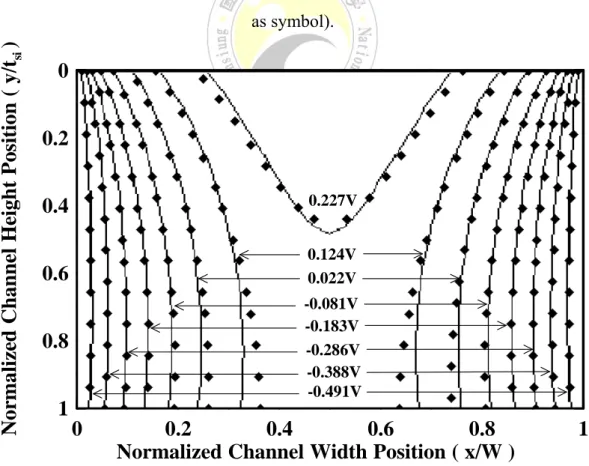
(33) 2.7 Potential Contour Fig. 2.11, Fig. 2.12, and Fig. 2.13 show the analytical potential contours and simulated data by the two-dimensional device simulator with variable channel width at W=60nm, W=80nm and W=120nm. A close agreement between them is observed, which further verifies the accuracy of our model. It is seen that the potential contours under the front gate bend vertically into the channel, which implies that the electric fields from the front gate will penetrate the channel and control the threshold behavior[24]. Among Fig. 2.11, Fig. 2.12 and Fig. 2.13, it can be seen that with the increase in the channel width of W, the potential contour value from the front gate in W=120nm is larger than W=60nm due to more vertical electric lines into the channel and less charge sharing effects at junction gate. The lateral coupling effects between the lateral gate and front gate for the four-gate transistor will increase the threshold voltage. Normalized Channel Height Position ( y/tsi ). related to front gate.. 0. 0.022V. 0.2. -0.081V. 0.4. -0.183V. 0.6. -0.286V -0.388V. 0.8. -0.491V. 1 0. 0.2 0.4 0.6 0.8 Normalized Channel Width Position ( x/W ). 1. Fig. 2.11 The analytical potential contours with channel width of W=60nm (defined as solid line) as well as those simulated by the two-dimensional device simulator (defined as symbol). 22.
(34) Normalized Channel Height Position ( y/tsi ). 0 0.124V. 0.2 0.022V. 0.4 0.6. -0.081V. 0.8. -0.183V -0.286V -0.388V -0.491V. 1 0. 0.2 0.4 0.6 0.8 Normalized Channel Width Position ( x/W ). 1. Fig. 2.12 The analytical potential contours with channel width of W=80nm (defined as solid line) as well as those simulated by the two-dimensional device simulator (defined. Normalized Channel Height Position ( y/tsi ). as symbol).. 0 0.2 0.4. 0.227V. 0.6. 0.124V 0.022V. 0.8. -0.081V -0.183V -0.286V -0.388V -0.491V. 1 0. 0.2 0.4 0.6 0.8 Normalized Channel Width Position ( x/W ). 1. Fig. 2.13 The analytical potential contours with channel width of W=120nm (defined as solid line) as well as those simulated by the two-dimensional device simulator (defined as symbol). 23.
(35) 2.8 Maximum Surface Potential In order to model the front gate threshold voltage (VT,G1), the terminal voltage VG1 and VG2 will be first linked to the maximum surface potential. From eq.(2.40), we define the front gate maximum surface potential as ψ 1,max and the back gate maximum surface potential as ψ 2,max . The maximum surface potential can be derived by setting. ∂ψ ( x, y = tsi ) ∂ψ ( x, y = 0) = 0 and = 0 . Accordingly, the position xmax1 and xmax2 of the ∂x ∂x maximum channel potential can be found by ⎛P ⎞ ln ⎜⎜ 1 ⎟⎟⎟ ⎜⎝ Q ⎠⎟ 1 xmax1 = xmax 2 = 2k1. (2.41). As xmax1 and xmax2 are solved, the maximum channel potential ψ 1,max andψ 2,max for the SOI G4-FET can be obtained as. ψ 1,max = b − 2 P1 × Q1 × sin(θ1 ) ψ 2,max =. −qN d 2 tsi + atsi + b − 2 P1 × Q1 × sin ( k1tsi + θ1 ) 2ε si. (2.42). (2.43). Fig. 2.14 shows the maximum front surface potential ψ 1,max related to the back -gate bias with the channel thickness as a parameter. It can be seen that when channel thickness is decreased from tsi=50nm to tsi=30nm, the maximum front surface potential are increased and with the coupling back gate effects, which induces back-gate surface into accumulated mode. It is observed that when channel thickness decreased, the back gate will easily turn to accumulated mode. In this section, our maximum channel potential model do not consider the coupling effects of back gate, yet. We will discuss this effect in section 2.8. Fig. 2.15 shows the maximum front surface potential ψ 1,max related to the back gate bias with the channel width as a parameter. It is observed that the increased of channel width will bring the raise of the maximum front surface potential and that accumulated operation of back gate is enhanced by the larger channel width due to the less lateral junction-gate effects.. 24.
(36) Maximum Surface Potential,Y1,max (V). 0.05 tox1 = 5 nm tox2 = 50 nm W=80 nm VJG = 0 V. 0. Symbol : ISE Solid line : Model. Vfb1=Vfb2=0.0 V Na = 1< 1020 cm-3 Nd=1< 1017cm-3. -0.05 -0.1. ’ : tsi=30nm & : tsi=40nm + : tsi=50nm. -0.15 -0.2 -0.25 0. 1. 2 3 Back-Gate Voltage ,VG2 (V). 4. 5. Fig. 2.14 The maximum front surface potential on the back-gate bias of VG2 bias for. Maximum Surface Potential,Y1,max (V). different channel thickness.. 0.4 tox1 = 5 nm tox2 = 50 nm. 0.2. 0. tsi =40 nm VJG = 0 V Vfb1=Vfb2=0.0 V Na = 1< 1020 cm-3 Nd=1< 1017cm-3. Symbol : ISE Solid line : Model + : W=60nm & : W=80nm ’ : W=120nm. -0.2. -0.4 -2. 0 2 Back-Gate Voltage ,VG2 (V). 4. Fig. 2.15 The maximum front surface potential on the back-gate bias of VG2 bias for different channel width.. 25.
(37) 2.9 Threshold Voltage Related to the Front Gate The threshold voltage related to the front and back gate is defined as the gate voltage which causes the maximum surface potential accumulation at the associated interface. From eq.(2.42) and eq.(2.43) we rewrite it as a linear equation related to VG1 and VG2.. ψ 1,max = Q × VG1 + T × VG 2 + U. (2.44). ψ 2,max = J × VG1 + F × VG 2 + G. (2.45). Using eq.(2.44) and eq.(2.45), we obtain VG1 =. F −T GT − FU ×ψ 1max + ×ψ 2max + QF − TJ QF − TJ QF − TJ. (2.46). VG 2 =. −J Q JU − QG ×ψ 1max + ×ψ 2max + QF − TJ QF − TJ QF − TJ. (2.47). Where Q = b1 − 2 A sin(θ1 ). (2.48). T = b2 − 2 B sin(θ1 ). (2.49). U = b3 − 2C sin(θ1 ). (2.50). J = a1tsi + b1 − 2 A sin(k1tsi + θ1 ). (2.51). F = a2tsi + b2 − 2 B sin(k1tsi + θ1 ). (2.52). G=−. qN D 2 tsi + a3tsi + b3 − 2C sin(k1tsi + θ1 ) 2ε si. (2.53). b1 =. tsiε ox + tox 2ε si tsiε ox + ε si (tox1 + tox 2 ). (2.54). b2 =. ε si tox1 tsiε ox + ε si (tox1 + tox 2 ). (2.55). with. b3 =. 2ε ox (−tsiε oxVFB1 − ε si tox 2VFB1 + ε si tox1VFB 2 ) + qN d tsi tox1 (tsiε ox + 2tox 2ε si ) 2ε ox (tsiε ox + ε si (tox1 + tox 2 )) a1 = a2 =. −ε ox tsiε ox + ε si (tox1 + tox 2 ). ε ox. tsiε ox + ε si (tox1 + tox 2 ) 26. (2.56) (2.57) (2.58).
(38) a3 =. 2(VFB1 − VFB 2 )ε oxε si + qN d tsi (tsiε ox + 2tox 2ε si ) 2ε si (tsiε ox + ε si (tox1 + tox 2 )). A= α1α 2 , B= β1β 2 , C= δ1δ 2. (2.60). α1 =. −4(η a1 + ρ b1 )(e KnW − 1) 2sinh( K nW ). (2.61). α2 =. 4(η a1 + ρ b1 )(e− KnW − 1) 2sinh( K nW ). (2.62). −4(η a2 + ρ b2 )(e KnW − 1) β1 = 2sinh( K nW ). (2.63). 4(η a2 + ρ b2 )(e − KnW − 1) 2sinh( K nW ). (2.64). β2 = (. δ1 =. 2qN d. ε si. γ − 4η a3 +4 ρ (VJG − φb − b3 ))(e K W − 1) n. (2.65). 2sinh( K nW ) (. δ2 =. (2.59). 2qN d. ε si. γ − 4η a3 +4 ρ (VJG − φb − b3 ))(−e − K W + 1) n. (2.66). 2sinh( K nW ). The threshold voltage model related to the front gate will be derived from eq.(2.44) and. eq.(2.45). by. assuming. symmetrical. junction-gate. bias. VJG1=VJG2=VJG.. Consequently, VT,G1 is obtained by imposing in eq.(2.44)ψ 1,max =0 and VG1= VT,G1 [12]. For an accumulated back surface, we obtain ψ 2,max =0 in eq.(2.44). For an inverted back surface, we have ψ 2,max = VJG + 2φF , where φF = −Vt ln( N d / ni ) is the Fermi potential of the n-type channel. For a depleted back surface, ψ 2,max is a function of both VG2 and VJG. By solving eq.(2.45) whileψ 1,max =0, we get depl = ψ 2max. QF − TJ JU − QG × VG 2 − Q Q. (2.67). Inserting eq.(2.67) into eq.(2.44) yields dep VT,G1 =. −T QF − TJ JU − QG GT − FU ×( × VG 2 − )+ QF − TJ Q Q QF − TJ. 27. (2.68).
(39) Fig. 2.16 shows the variation of the threshold voltage related to the front gate with the back-gate bias for the different junction-gate biases. The results predicted by the model from symmetrical junction-gate case are clearly demonstrated in this figure. The threshold voltage is extracted from ISE simulations as the gate voltage at which the surface accumulation electron concentration becomes equal to the body doping. It can be seen that as the junction-gate bias is decreased from VJG=0 V to VJG=-3 V, the threshold voltage is increased correspondingly due to the channel is heavily depleted by the more negative junction-gate bias, which causes essential high front-gate bias to accumulate the electron near the surface and result in the increase in the threshold voltage. Also, when the back-gate bias of VG2 is increased toward the positive value to make the back surface become accumulated, the threshold voltage is obviously pulled down to the minimum value. This is because the positive back-gate bias efficiently assist the front interface to reach accumulated conduction and hence a small threshold voltage for the front-gate can turn on the channel. This is called positive vertical coupling effects (PVCEs) between the positive bottom gate and front gate, which decreases the threshold voltage related to the front gate.. 3.2 tox1 = 5 nm Vfb1=Vfb2=1.18 V 20 -3 tox2 = 50 nm Na = 1< 10 cm Nd=1< 1017cm-3 t = 40nm. Threshold Voltage, VT,G1(V). VJG = -3 V. 2.8. si. W=80 nm. VJG = -2 V. 2.4 2 1.6. Dash line : ISE Solid line : Model. VJG = -1 V. VJG = 0 V. 1.2 -20. -10 0 10 Back-Gate Voltage ,VG2 (V). 20. Fig. 2.16 The variation of the threshold voltage related to the front gate with the back-gate bias for the different junction gate biases. 28.
(40) On the contrary, when the back-gate bias is decreased toward the negative value to make back surface become inverted, the threshold voltage is obviously pulled up to the maximum value. It implies that the negative back-gate bias can effectively resist the front interface to accumulate the majority carrier and hence the large front-gate bias is needed to reach the turn-on condition. This is called negative vertical coupling effects (NVCEs) between the negative bottom gate and front gate that increases the threshold voltage related to the front gate. Note that both PVCEs and NVCEs can be intensively enhanced when the junction-gate become more negative. It is worthwhile to point out that the much more discrepancy of our model from the device simulator for the larger junction-gate bias |VJG| mainly caused by the non-linear potential distribution in the back oxide. When junction-gate bias |VJG| become larger and larger, the predominant of electric field in back oxide between back gate bias and junction-gate bias will be unpredictable. This will cause the threshold voltage increase to a certain level to shorten the discrepancy between our model and device simulator. Beside the threshold voltage. Threshold Voltage, VT,G1(V). degradation caused by the gate coupling between the front gate and back gate,. ’ : tsi=30nm Symbol : ISE & : tsi=40nm Solid line : Model Dash line :Ref.[12] + : tsi=50nm. 1.4. 1.3. 1.2 tox1 = 5 nm tox2 = 50 nm W=80 nm VJG1 = 0 V VJG2 = 0 V. 1.1. Vfb1=Vfb2=1.15 V Na = 1< 1020 cm-3 Nd=1< 1017cm-3. 1 0. 1. 2 3 Back-Gate Voltage ,VG2 (V). 4. 5. Fig. 2.17 The variation of the threshold voltage related to the front gate with the channel thickness of tsi.. 29.
(41) Fig. 2.17 shows how the channel thickness of tsi affects the threshold voltage related to the front gate. The simulation results of the parabolic approach [12] are also included for comparison. It shows that as the channel thickness is shrunk, the threshold voltage can be reduced due to an early onset of accumulation for the decrease in the total depletion charge under the gate with decrease in the channel thickness. Our model is superior to the previous model for a close proximity with the simulation results. When the back-gate bias is increased from 0 V to 5 V for some channel thickness, the PVCEs. Threshold Voltage, VT,G1(V). is enhanced and the threshold voltage is decreased consequently.. Symbol : ISE Solid line : Model Dash line :Ref.[12]. 1.6. 1.4. 1.2. 1. 0.8 -2. tox1 = 5 nm tox2 = 50 nm tsi = 40 nm Vfb1=Vfb2=1.14 V 20 -3 VJG1 = 0 V Na = 1< 10 cm VJG2 = 0 V Nd=1< 1017cm-3. -1. ’ : W=60nm & : W=80nm + : W=120nm. 0 1 2 3 Back-Gate Voltage ,VG2 (V). 4. 5. Fig. 2.18 The dependence of the threshold voltage related to the front gate on the back-gate bias with the channel width as a parameter. Fig. 2.18 shows the dependence of the threshold voltage related to the front gate on the back-gate bias with the channel width as a parameter. It can be seen that the narrow channel width of W=60 nm will result in the strong electric coupling between the junction gate and the front gate and causes the strong LCEs that stops some of the electric fields of the front gate from going into the channel and as a result of the increased threshold voltage. When the back-gate bias is decreased from 5 V to -2 V for. 30.
(42) some channel width, the NVCEs is enhanced and the threshold voltage is increased consequently.. 2.10 Results and Discussion Based on the exact solution of 2-D Poisson equation, a new analytical model comprising the potential distribution and threshold voltage for the fully depleted SOI four-gate transistor has been developed. To keep the threshold voltage stable as the device scaled down to deep-submicrometer regime for the VLSI application, we should seriously consider both the device structure parameters such as W and tsi and the device bias conditions such as VG2< 0 V, VG2> 0 V and VJG<0V to well control all effects of LCEs, NVCEs, and PVCEs that may cause the degradation of the threshold voltage related to the front gate. The good simulation results of the model make it useful for predicting the device threshold behavior and potential distribution and offer the guidance for the basic design SOI G4-FET. With appropriate modification, the model can be extended to the modeling of the conventional SOI MOSFET's. 31.
(43) Chapter 3 THREE DIMENSIONAL MODEL FOR SOI FOUR-GATE TRANSISTER 3.1 Model Derivation The n-channel G4-FET is shown in Fig. 3.1, the symbols and axes used for modeling are indicated. We consider the same assumption as the 2-D model that impurity density in the channel region is uniform and neglecting the effect of the fixed oxide charges on the electrostatics of the channel. The channel potential distribution is expressed by ψ ( x, y, z ) . Assume that the channel region is fully-depleted. According to the Poisson equation, the channel potential distribution can be written as eq.(3.1) [25]. qN ∂ 2ψ ( x, y, z ) ∂ 2ψ ( x, y, z ) ∂ 2ψ ( x, y, z ) + + =− d 2 2 2 ∂x ∂y ∂z ε si. 0 ≤ x ≤ W , 0 ≤ y ≤ t si , 0 ≤ z ≤ L (3.1). Fig. 3.1 The structure of n-channel G4-FET. 32.
(44) Where Nd is the uniform film doping concentration independent of the gate length, tox1 is the gate oxide thickness, tox2 is the buried oxide thickness, tsi is the silicon film thickness, and W is the device channel width, L is the device channel length and the y-axis is vertical to the channel thickness, the x-axis is parallel to the channel width and z-axis presents the channel length, respectively. By using the superposition method, the resultant solution ψ ( x, y, z ) can be decomposed with one-dimensional (1-D) potential solution V(y), 2-D potential solution U(x,y) and 3-D potential solution T(x,y,z) at eq.(3.2) which satisfy the following 3-D Laplace equation, 2-D Laplace equation and 1-D Poisson equation, respectively[26].. ψ ( x, y, z ) = V (y) + U ( x, y )+T ( x, y,z). (3.2). Substituting eq.(3.2) into eq.(3.1), we obtain qN ∂ 2U ( x, y ) ∂ 2T ( x, y,z) ∂ 2V (y) ∂ 2U ( x, y ) ∂ 2T ( x, y,z) ∂ 2T ( x, y,z) + + + + + =− d 2 2 2 2 2 2 ∂x ∂x ∂y ∂y ∂y ∂z ε si (3.3) 1-D Poisson equation ∂ 2V ( y ) −qN d = ∂y 2 ε si. (3.4). 2-D Laplace equation ∂ 2U ( x, y ) ∂ 2U ( x, y ) + =0 ∂x 2 ∂y 2. (3.5). 3-D Laplace equation. ∂ 2T ( x, y,z) ∂ 2T ( x, y,z) ∂ 2T ( x, y,z) + + =0 ∂x 2 ∂y 2 ∂z 2. 33. (3.6).
(45) 3.2 3-D Boundary Conditions Value Problem The Poisson equation is solved by using the following boundary conditions: (A) At the top side, electric flux at the interface of silicon/gate oxide is continuous ∂ψ (x, y,z) ∂y. y =0. =−. ε ox VGS1 − VFB1 −ψ (x, y,z) × tox1 ε si. (0 ≤ x ≤ W,0 ≤ z ≤ L). (3.7). Where VGS1 is the top gate bias refers to source bias, tox1 is the gate oxide thickness, εsi is permittivity of silicon, εox is permittivity of oxide, and VFB1 is the flat-band voltage of front bias given as the difference between front gate material work function and silicon work function. (B) At the bottom side, electric flux at the interface of silicon/buried oxide is continuous ∂ψ (x, y,z) ∂y. y =tsi. =. ε ox VGS2 − VFB 2 −ψ (x, y,z) × tox2 ε si. (0 ≤ x ≤ W,0 ≤ z ≤ L). (3.8). Where VGS2 is the bottom gate bias refers to source bias, VFB2 is the flat-band voltage of back gate, tox2 is the back oxide thickness. (C) The potential at the VJG1 end is. ψ (0, y,z) = VJG1 -φb. (0 ≤ y ≤ t si , 0 ≤ z ≤ L). (3.9). (D) The potential at the VJG2 end is. ψ (W, y,z) = VJG2 -φb. (0 ≤ y ≤ t si , 0 ≤ z ≤ L). (3.10). Where φb is the potential barrier between the junction-gates and the channel (=Eg/2+VTln(Nd/ni)) [12]. (E) The potential at the source end is. ψ (x, y,L) = Vbi. (0 ≤ x ≤ W , 0 ≤ y ≤ t si ). (3.11). (F)The potential at the drain end is. ψ (x, y,0) = Vbi +VDS. (0 ≤ x ≤ W , 0 ≤ y ≤ t si ). 34. (3.12).
(46) Note that (B), for the thick buried oxide, we need to use the effective back-gate bias to compensate the non-linearity of the potential distribution in the buried gate oxide[22]. Fig. 2.2 shows the 3-D simulated potential variation of ψ(x=W/2,y,z=L/2) with VGS2=0V and VGS2=3V and the effective substrate bias of VGeff2 is also included for comparison. The potential dose not vary linearly inside the buried oxide at VG2=0V as the same in 2-D model, which due to the influence of the junction gates electric fields. But when VG2>0, the variation of potential with the back-gate bias will gradually become linear, it is because the back gate bias effect alleviate the junction gates electric fields or even be predominant. To account for this nonlinearity, we use a modified boundary condition, where an effective back-gate voltage VGeff2 [22] is introduced. ∂ψ (x, y,z) ∂y. y = tsi. =. ε ox VGSeff2 − VFB 2 −ψ (x, y,z) × ε si tox2. (0 ≤ x ≤ W,0 ≤ z ≤ L). (3.13). VGSeff2 is defined by eff V GS 2 = VGS 2 + ψ (W / 2, y , L / 2) + tox 2 × (. 0. y = tox1 + tsi. Dash line : Model with effective substrate bias Solid line: ISE. 20 Silicon film. 30. Na = 1< 1020 cm-3 Nd=1< 1017cm-3. 40 50. BOX. 60 70 80 90 -1. (3.14). GOX. 10 Device Height, y (nm). ∂ψ (W / 2, y, L / 2) ) ∂y. VG2=0V. VG2=1V. VG2=2V. VG2=3V. tox1 = 5 nm tox2 = 50 nm tsi = 40 nm W=80 nm L=240 nm VGS1 = 0 V VJG = 0 V. 0 1 2 Potential, Y(x=W/2,y,L/2) (V). Fig. 3.2 The simulated potential variation of ψ(x=W/2,y,z=L/2) with VGS2=0V and VGS2=3V and the effective substrate bias of VGeff2 is also included for comparison. 35. 3.
(47) 3.3 1-D and 2-D Solution From boundary condition (A) and (B), we get ∂V ( y ) ∂y. ∂V ( y ) ∂y. =− y =0. = y = tsi. ε ox VGS 1 − VFB1 − V ( y ) × tox1 ε si. (3.15). ε ox VGS2 − VFB 2 − V ( y ) × ε si tox2. (3.16). Using eq.(3.15) and eq.(3.16), 1-D solution can be obtained as qN d 2 y + ay + b 2ε si. V ( y) = −. (3.17). Where a=. b=. 2 (VFB1 − VFB 2 − VGS 1 + VGS 2 ) ε oxε si +qN d tsi ( tsiε ox + 2tox 2ε si ). (3.18). 2ε si ( tsiε ox + ε si ( tox1 + tox 2 ) ). {. }. 2ε ox tsiε ox (VGS 1 − VFB1 ) − ε si ⎡⎣tox 2 (VFB1 − VGS 1 ) + tox1 (VFB 2 − VGS 2 ) ⎤⎦ +qN d tsi tox ( tsiε ox + 2tox 2ε si ) 2ε ox ( tsiε ox + ε si ( tox1 + tox 2 ) ). (3.19) Using separation method together with boundary condition which the same as chapter 2, one obtains the solution of the two-dimensional Laplace equation. ∞. (. ). U ( x, y ) = ∑ Pn e − kn x + Qn ekn x sin ( kn y + θ n ) n =1. (3.20). Where tan kntsi = tan θ n =. ε oxε si kn ( tox1 + tox 2 ) ε si 2 kn 2tox1tox 2 − ε ox 2. (3.21). ε si tox1kn ε ox. (3.22). 36.
(48) 3.4 3-D Laplace Equation Solution By using separation method together with boundary condition, one obtains the following resultant solution of the three-dimensional Laplace equation. From eq.(3.6) we let T ( x, y, z ) = X ( x)Y ( y ) Z ( z ). (3.23). Substitute eq.(3.23) into eq.(3.6) to obtain X '' ( x)Y ( y ) Z ( z ) + X ( x)Y '' ( y ) Z ( z ) + X ( x)Y ( y ) Z '' ( z ) = 0. (3.24). eq.(3.24) divide by X ( x)Y ( y ) Z ( z ) X '' ( x) Y '' ( y ) Z '' ( z ) + + =0 X ( x) Y ( y ) Z ( z ). (3.25). By letting X '' ( x) Y '' ( y ) Z '' ( z ) = −k12 , = − k2 2 , = k12 + k2 2 X ( x) Y ( y) Z ( z). (3.26). X ( x) = a1cos(k1 x) + a2 sin(k1 x). (3.27). Y ( y ) = a3cos (k2 y ) + a4 sin(k2 y ). (3.28). We obtain. Z ( z ) = a5e − (. k12 + k22 ) z. + a6 e(. k12 + k22 ) z. (3.29). From (C) and (D), we let T(0,y,z)=0 and T(W,y,z)=0 as boundary condition for eq.(3.27) to obtain X ( x) = a2 sin(km x) , km =. mπ , m = 1, 2,3... W. (3.30). Using a3cos (k2 y ) + a4 sin( k2 y ) = a32 + a42 sin ( k2 y + θ ) , eq.(3.23) can be rewrite as ∞. ∞. T ( x, y,z) = ∑∑ a32 + a4 2 × a2 sin ( km x ) sin ( kn y + θ n ) (a5e n =1 m =1. − ( km 2 + k n 2 ) z. + a6 e. ( k m 2 + kn 2 ) z. ). (3.31) 37.
(49) Let a32 + a4 2 × a2 × a5 = Rmn ,. a32 + a4 2 × a2 × a6 = Fmn. (3.32). We obtain ∞. ∞. (. ). T ( x, y,z) = ∑∑ Rmn e − kmn z + Fmn e kmn z sin ( km x ) sin ( kn y + θ n ) n =1 m =1. (3.33). Where kmn2 = km2+kn2, θ n is triangular parameters. From boundary condition (A) and (B), one obtain ∂T (x, y,z) ∂y. ∂T (x, y,z) ∂y. = y =0. ε ox T (x, y,z) × ε si tox1. = y = tsi. ε ox −T (x, y,z) × tox2 ε si. (3.34). (3.35). Using eq.(3.34) and (3.35), we obtain tan kntsi = tan θ n =. ε oxε si kn ( tox1 + tox 2 ) ε si 2 kn 2tox1tox 2 − ε ox 2. (3.36). ε si tox1kn ε ox. (3.37). 38.
(50) 3.5 Coefficients Solution The resultant solution of the two-dimensional Laplace equation at eq.(3.20).Where the Fourier series coefficients of Pn, Qn, Cn and Dn, are expressed as Cn e KnW − Dn 2sinh( K nW ). (3.38). −Cn e − KnW + Dn 2sinh( K nW ). (3.39). Pn = Qn = with Cn =. u1. (3.40). Dn =. u2. (3.41). sin(2θ n ) − sin(2( kntsi + θ n )) + 2kntsi 4k n. (3.42). α. α. Where u1,u2 and α. α=. u1 =. q × Nd × ς − a × σ + (VJG1 − φb − b ) ×ϖ 2ε si. (3.43). u2 =. q × Nd × ς − a × σ + (VJG 2 − φb − b ) ×ϖ 2ε si. (3.44). and ς ,σandωin above equations are defined as. ς=. −2 cos(θ n ) + 2 cos(kntsi + θ n ) + kntsi (2sin(knt si + θ n ) − cos(knt si + θ n )kntsi ) kn3. (3.45). σ=. − sin(θ n ) + sin(kntsi + θ n ) − cos(kntsi + θ n )kntsi kn 2. (3.46). ϖ=. cos(θ n ) − cos(kn tsi + θ n ) kn. (3.47). 39.
(51) The resultant solution of the three-dimensional Laplace equation at eq.(3.33). Where the Fourier series coefficients of Amn, Bmn, Rmn and Fmn are expressed as Rmn =. Amn e kmn L − Bmn 2sinh(kmn L). − Amn e − kmn L + Bmn Fmn = 2sinh(kmn L). (3.48). (3.49). Amn =. 4(− β + β (−1) m + αδ km ) α (−2mπ ). (3.50). Bmn =. 4(−τ + τ (−1) m + αδ km ) α (−2mπ ). (3.51). β=. qN D × ς − a × σ + (Vbi +VDS − b ) ×ϖ 2ε si. (3.52). τ=. qN D × ς − a × σ + (Vbi − b ) ×ϖ 2ε si. (3.53). km (Cn − (−1) m Dn ) kmn 2. (3.54). δ=. Fig. 3.3 shows the decay of Fourier series Rmn coefficients versus the term number. Since the Fourier series coefficients decay rapidly, the first term of Rmn will dominate the whole series and be used to derive the threshold voltage according to the minimum surface potential[25].. 40.
(52) Coefficient (Rmn). 1.2 tox1 = 5 nm tox2 = 50 nm tsi = 40 nm VGS1 = 0 V VGS2 = 0V VJG = 0 V. 0.8. Vfb1=Vfb2=0 V Na = 1< 1020 cm-3 Nd=1< 1017cm-3 L=240 nm W=80 nm. 0.4. 0. -0.4 0. 20. 40 60 Term Number, mn. 80. Fig. 3.3 The decay of Fourier series Rmn coefficients versus the term number.. 41. 100.
(53) 3.6 3-D Generalized Potential Model The full expression for the potential in silicon channel region is. ψ ( x, y, z ) = V (y) + U ( x, y )+T ( x, y,z) =. ∞ −qN d 2 y + ay + b + ∑ Pn e − kn x + Qn e kn x sin ( kn y + θ n ) 2ε si n =1. (. ∞. ∞. (. ). (3.55). ). + ∑∑ Rmn e − kmn z + Fmn e kmn z sin ( km x ) sin ( kn y + θ n ) n =1 m =1. To verify the analytical body potential model, we will show the 3-D potential distribution by 3-D simulator of ISE [14] and model solution at different cross-section with xmax, top gate surface of y=0 and zmin of variable biases. In Fig. 3.4 and Fig. 3.5 show the 3-D potential distribution from the device simulator and model results with the same device structure at zmin and bias condition for symmetrical junction-gate device with VJG1= VJG2=0V. Fig. 3.6 and Fig. 3.7 show the 3-D device simulator and model results at zmin for asymmetrical VJG1=0V, VJG2=-1V, respectively. Fig. 3.8 and Fig. 3.9 show the 3-D device simulator and model results at top gate surface for VDS=0V. Fig. 3.10 and Fig. 3.11 show the 3-D device simulator and model results at top gate surface for VDS=0.5V. It is obviously seen that a close agreement for the 3-D potential distribution between the device simulator and analytical model are obtained. Fig. 3.12 shows the variation of the surface potential ψ(x,y=0,zmin) and ψ(x,y=tsi,zmin) with the normalized channel width position x/W for the different junction-gate biases and the effective substrate bias of VGSeff2 is also included for comparison. A good agreement between the results calculated from our model with those simulated using the device simulator is obtained. It is observed that when the junction-gate bias of VJG2 is decreased from 0V to -1V, the maximum potential for both surface at y=0 and y=tsi are decreased. The reduced maximum surface potential will make it more difficult for the majority carrier to accumulate near the surface and will pull up the threshold voltage. Fig. 3.13 shows the variation of the channel potential ψ(x,y,zmin) with the normalized channel height position y/tsi for the different channel locations and the effective substrate bias of VGSeff2 is also included for comparison. It can be seen that at the middle of the channel of x=40nm, the surface potential of ψ(x,y=0,zmin) and ψ(x,y=tsi,zmin) is much larger than 42.
(54) that for the location of x=10nm and x=20nm. It implies that the device turn-on point will easily occurs at the middle of the surface due to easier accumulation operation for the larger surface potential happening at x=40nm=W/2 which corresponds to the equation of xmax= W/2=ln(P1/Q1)/2k1. Fig. 3.12 shows the variation of the surface potential ψ(xmax,y=0,z) and ψ(x,y=tsi,z) with the normalized channel length position z/L for the different drain biases of VDS=0V and VDS=0.5V. It is observed that when the drain bias of VDS is increased from 0V to 0.5V, the minimum potential for both surface at y=0 and y=tsi are pull up. The reduced minimum surface potential will make it more easily for the majority carrier to accumulate near the surface and will decrease the threshold voltage that cause drain-induced barrier-lowering. Fig. 3.15 shows the variation of the channel potential ψ(xmax,y,z) with the normalized channel height position y/tsi for the different channel locations of z=30nm, z=60nm, and z=120nm and the effective substrate bias of VGSeff2 is also included for comparison. It can be seen that at the middle of the channel length of z=120nm, the surface potential of ψ(xmax,y=0,z) and ψ(xmax,y=tsi,z) is much smaller than that for the location of z=60nm and z=30nm. It implies that the device turn-on point will difficultly occurs at the middle of the surface due to difficult accumulation operation for the smaller surface potential happening at z=120nm=L/2 which corresponds to the equation of zmin = L/2=ln(R11/F11)/2k11.. 43.
(55) Fig. 3.4 The 3-D potential distribution from the device simulator of ISE for symmetrical junction-gate device VJG1= VJG2=0V at zmin.. Fig. 3.5 The 3-D potential distribution from model results for symmetrical junction-gate device VJG1= VJG2=0V at zmin.. 44.
(56) Fig. 3.6 The 3-D potential distribution from the device simulator of ISE for asymmetrical junction-gate device VJG1= 0V, VJG2=-1V at zmin.. Fig. 3.7 The 3-D potential distribution from model results for asymmetrical junction-gate device VJG1= 0V, VJG2=-1V at zmin.. 45.
(57) Fig. 3.8 The 3-D potential distribution at top gate surface from the device simulator of ISE for VDS= 0V.. Fig. 3.9 The 3-D potential distribution at top gate surface from model results for VDS= 0V.. 46.
(58) Fig. 3.10 The 3-D potential distribution at top gate surface from the device simulator of ISE for VDS = 0.5V.. Fig. 3.11 The 3-D potential distribution at top gate surface from model results for VDS= 0.5V.. 47.
(59) 0 Potential, Y (x,y,zmin)(V). y=0. -0.4 -0.8 y=tsi tox1 = 5 nm tox2 = 50 nm tsi = 40 nm VGS1 = 0 V VGS2 = 0V VJG1 = 0 V. -1.2 -1.6. Vfb1=Vfb2=0 V Na = 1< 1020 cm-3 # : VJG2=0V Nd=1< 1017cm-3 & : VJG2=-1V Nd+=1< 1020cm-3 Symbol : ISE Solid line : Model L= 240 nm Dash line : Model with effective W= 80 nm substrate bias. -2 0. 0.2. 0.4. 0.6. 0.8. 1. Normalized Channel Width Position , (x/W) Fig. 3.12 The variation of the surface potential of ψ(x,y=0,zmin) and ψ(x,y=tsi,zmin) with the normalized channel width position x/W for the different junction-gate biases of VJG2=-1V and VJG2=0V and the effective substrate bias of VGSeff2 is also included for comparison. # : x=40nm &: x=20nm +: x=10nm. -0.2. min. Potential, Y(x,y,z ) (V). 0. -0.4. tox1 = 5 nm Vfb1=Vfb2=0 20 -3 Na = 1< 10 cm tox2 = 50 nm Nd=1< 1017cm-3 tsi =40 nm Nd+=1< 1020cm-3 W=80 nm L=240 nm Symbol : ISE Solid line : Model Dash line : Model with effective substrate bias. VGS1 = 0 V VGS2 = 0V VJG1 = 0 V VJG2 = 0 V. -0.6. -0.8 0. 0.2 0.4 0.6 0.8 Normalized Channel Height Position , (y/tsi). 1. Fig. 3.13 The variation of the channel potential of ψ(x,y,zmin) with the normalized channel height position y/tsi for the different channel locations of x=10nm, x=20nm and x=40nm and the effective substrate bias of VGSeff2 is also included for comparison. 48.
(60) Symbol : ISE tox 1 = 5 nm Solid line : Model Dash line : Model with effective tox2 = 50 nm tsi = 40 nm substrate bias VGS1 = 0V & : VDS=0V VGS2 = 0V # : VDS=0.5V VJG1 = 0V VJG2 = 0V. 0.4. max. Potential, Y(x ,y,z) (V). 0.8. 0. Vfb1=Vfb2=0 V Na = 1< 1020 cm-3 Nd=1< 1017cm-3 Nd+=1< 1020cm-3 W=80 nm L =240 nm. y=0. -0.4. y=tsi. -0.8 0. 0.2. 0.4. 0.6. 0.8. 1. Normalized Channel Length Position , (z/L) Fig. 3.14 The variation of the surface potential of ψ(xmax,y=0,z) and ψ(xmax,y=tsi,z) with the normalized channel length position z/L for the different drain biases of VDS=0V and VDS=0.5V and the effective substrate bias of VGSeff2 is also included for comparison.. max. Potential, Y(x ,y,z) (V). -0.1 Symbol : ISE Solid line : Model Dash line : Model with effective substrate bias. -0.2 -0.3 tox1 = 5 nm tox2 = 50 nm tsi =40 nm W=80 nm L=240 nm VGS1 = 0 V VGS2 = 0V VJG1 = 0 V VJG2 = 0 V. -0.4 -0.5 -0.6 0. Vfb1=Vfb2=0 Na = 1< 1020 cm-3 # : z= 120nm Nd=1< 1017cm-3 & : z= 60nm Nd+=1< 1020cm-3 + : z= 30nm. 0.2. 0.4. 0.6. 0.8. 1. Normalized Channel Height Position , (y/tsi) Fig. 3.15 The variation of the channel potential of ψ(xmax,y,z) with the normalized channel height position y/tsi for the different channel locations of z=30nm, z=60nm and z=120nm and the effective substrate bias of VGSeff2 is also included for comparison. 49.
數據
+7

Outline
相關文件
Then, we recast the signal recovery problem as a smoothing penalized least squares optimization problem, and apply the nonlinear conjugate gradient method to solve the smoothing
O.K., let’s study chiral phase transition. Quark
This kind of algorithm has also been a powerful tool for solving many other optimization problems, including symmetric cone complementarity problems [15, 16, 20–22], symmetric
雙極性接面電晶體(bipolar junction transistor, BJT) 場效電晶體(field effect transistor, FET).
Therefore, in this research, we propose an influent learning model to improve learning efficiency of learners in virtual classroom.. In this model, teacher prepares
Finally, we use the jump parameters calibrated to the iTraxx market quotes on April 2, 2008 to compare the results of model spreads generated by the analytical method with
In Section 4, we give an overview on how to express task-based specifications in conceptual graphs, and how to model the university timetabling by using TBCG.. We also discuss
情境感知巡檢路線即時導引機制之研製 Development of a Real-time Patrol Routing Mechanism in a Context-Aware Environment
In the proposed method we assign weightings to each piece of context information to calculate the patrolling route using an evaluation function we devise.. In the
