Abstract—The performance of thin-film transistors with a novel poly-Si nanowire channel prepared by solid-phase crystallization is investigated in this paper. As compared with conventional planar devices having self-aligned source/drain, the new devices show an improvedON-current per unit width and better control over the short channel effects. The major conduction mechanism of the
OFF-state leakage is identified as the gate-induced drain leakage, and it is closely related to the source/drain implant condition and the unique device structure.
Index Terms—Leakage, nanowires (NWs), plasma hydrogena-tion, poly-Si, short-channel effect, thin-film transistor (TFT).
I. INTRODUCTION
M
INIMIZATION of silicon devices is being actively pur-sued. In this regard, Si nanowires (NWs) possess great potential for testing and understanding fundamental role of dimensionality and size in device electrical properties. Owing to its inherent high surface-to-volume ratio, NWs can effec-tively suppress the short-channel effects normally encountered in nanoscale MOSFETs [1] and provide high surface sensitivity for sensing devices. Many potential applications of Si NWs have been investigated, including nano CMOS [1], novel logic devices [2], memory devices [3], NW thin-film transistors (TFTs) [4], biosensors [5], [6], and nanoelectromechanical switch devices [7].Si NWs could be prepared by either top–down methods using advanced lithographic tools like deep UV steppers [1], [3] and e-beam writers [6], or bottom-up methods with catalyst-assisted growth [4], [5]. The former approach, albeit well developed and mature for mass-production purpose, is costly as it requires ex-pensive equipments and cutting-edge technologies. By contrast, the latter approach is flexible for experimental studies, although potential concerns like metal contamination, positioning of the NWs [8], and the control of structural parameters such as NW’s
Manuscript received January 16, 2006; revised July 10, 2006. This work was supported in part by the National Science Council, Taiwan, R.O.C., under Contract of NSC-94-2120-M-009-017. The review of this paper was arranged by Editor M. Reed.
H.-C. Lin is with the Institute of Electronics, National Chiao-Tung Uni-versity, Hsinchu, Taiwan, R.O.C. and also with the National Nano Device Laboratories, Hsinchu 300, Taiwan, R.O.C.
M.-H. Lee and C.-J. Su are with the Institute of Electronics, National Chiao-Tung University, Hsinchu, Taiwan, R.O.C.
S.-W. Shen is with the National Nano Device Laboratories, Hsinchu 300, Taiwan, R.O.C.
Digital Object Identifier 10.1109/TED.2006.882033
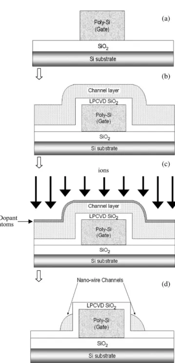
Fig. 1. (a) Structure of the NW device. (b) Cross-sectional view of the NW channels and the gate.
diameter, length, and orientation [9] could eventually hinder its use in practical manufacturing.
Recently, we proposed and demonstrated a novel method to fabricate NW TFTs [10]. The method is simple and com-patible with modern semiconductor process steps. Moreover, it does not require costly lithographic tools. In this paper, we further investigate the characteristics of the new NW devices by applying solid-phase crystallized (SPC) poly-Si channels. Performance comparisons with conventional planar devices, effects of plasma treatment, and the conduction mechanism of theOFF-state leakage current are explored and addressed.
II. DEVICESTRUCTURE ANDFABRICATION
Fig. 1 shows a schematic structure of the proposed NW de-vice. It adopts a side-gate scheme where two NW channels are formed on the sidewall of the gate. Source and drain (S/D) re-gions lying across the gate are defined simultaneously with the formation of NW channels in a self-aligned manner, which will
Fig. 2. Key device-fabrication flow.
be described later. Another unique feature of the new structure is that a large portion of the NW is inherently exposed to the environment, which serves seamlessly as the sensing site when the device is used as a sensor. For example, for biologic sensor applications, the exposing NW surface serves as the sensing site, and after certain immobilization treatment, specific recep-tor agents are formed on the surface, which could selectively detect the target species contained in the test solution [5], [6].
The fabrication process is briefly illustrated in Fig. 2. Details about the fabrication could be found in our previous work [10]. To investigate the effectiveness of plasma passivation, some samples were treated in NH3plasma at 300◦C after the metallization steps. All the devices characterized in this paper are with a gate oxide of 30 nm.
21 and 23 nm, respectively.
Fig. 4. Measured NW width and thickness as a function of the overetch time.
Fig. 3 depicts a picture taken by transmission electron microscopy (TEM), showing an NW channel formed on the sidewall of a gate after plasma etching. In this example, the NW thickness and width [see the definition shown in Fig. 1(b)] are 21 and 23 nm, respectively. Since the device adopts a side-gate scheme, the NW width represents the width of the conduction channel. Fig. 4 illustrates the trends, in which both NW thick-ness and width decrease with overetch time as characterized by TEM. In this figure, the film thickness before etching was 100 nm. The results indicate that the structural parameters of the NW devices could be controlled reasonably. In other words, by carefully controlling the thickness of the deposited channel film and the overetch time, the structure can be easily shrunk into nanoscale regime.
To illustrate the impacts of using the NW channels on the device performance, control devices with conventional top-gate and self-aligned S/D structure were also fabricated. These control devices have a 50-nm thick SPC channel treated with the same SPC conditions as the NW split and also received a plasma treatment in NH3plasma at 300◦C for 1 h.
III. CHARACTERISTICS OF THEFABRICATEDDEVICES
Threshold voltage (Vth) and drain current (Id) of the fabri-cated devices as a function of channel length (L) are shown in Figs. 5 and 6, respectively. As shown in Fig. 5, the plasma treatment results in a significant reduction in Vth, indicating an effective passivation of the traps contained in the channel after the treatment. Fluctuation in the parameters becomes more obvious as the channel becomes shorter. This is reasonable and is related to the inherent grain structure contained in the
Fig. 5. Threshold voltage (Vth) as a function of channel length for NW
devices with and without receiving plasma treatment. The number of devices characterized under each condition is 50.
Fig. 6. ON-current as a function of the channel length for NW devices with and without receiving plasma treatment. The currents were measured at
VG= 10 V and VD= 3 V. The number of devices characterized under each
condition is 50.
channels [11]. As the channel dimensions approach the grain size, the variation in the number of grain boundaries would greatly affect the device performance, resulting in larger fluc-tuation of device characteristics.
On the other hand, ON-current increases reasonably with a decreasing channel length, as shown in Fig. 6. After the plasma treatment, the current is dramatically improved. This is due to the reduction of Vthas well as an improved mobility after passivation, and could be understood by the results shown Fig. 7, in which the subthreshold characteristics of the NW transistors with and without plasma treatments are compared. Dramatic improvement in the device performance in terms of drastically reduced Vth, steeper subthreshold slope, higher Id, and reduced leakage, is achieved with the plasma treatment. Detailed device parameters are listed in Table I.
Fig. 8 compares the Vth of NW devices with that of the conventional planar SA structure as a function of channel length. As shown in the figure, Vth rolloff is obvious for the control split as the channel length is shorter than 2 µm, while the NW devices exhibit only weak dependence on the channel length. This comparison reflects the high surface-to-volume feature of the NWs mentioned above, which tends to enhance the gate controllability. As the source-to-drain leakage current
Fig. 7. Subthreshold characteristics of NW devices with and without receiving plasma treatment.
TABLE I
MAJORPERFORMANCEPARAMETERS FOR THENW DEVICES
CHARACTERIZED INFIG. 7
Fig. 8. Threshold voltage (Vth) as a function of channel length for reference
and NW devices. Channel thickness of the reference device is 50 nm. The channel width is 20 µm for reference devices and 21 nm for the NW devices. These devices received a treatment in a NH3plasma for 1 h. The number of
devices characterized for each condition is 20.
via the body of the channel is effectively suppressed in the NW devices by thinning the NW thickness, good control over the short-channel effect could be achieved.
To more clearly illustrate the impact of using the NWs as the channel, Fig. 9 depicts the subthreshold characteristics of devices with various channel width. Note that, the drive current is normalized to the width. The results indicate that the shrinkage of the channel dimensions could help improve the device performance in terms of higherON-current and steeper subthreshold slope. To help understand this impact, we use the illustrations shown in Fig. 10 to analyze the geometry difference of the proposed NW with that of conventional planar
Fig. 9. Drain current per unit width as a function of channel width for control and NW devices. The number of devices characterized under each condition is 20.
Fig. 10. Schematic drawings of the cross section of (a) the triangle NW and (b) conventional planar structure along the width direction.
structure. Here, the cross section of the NW is assumed to have a triangular shape with an area of 1/2(WNW• TNW), as shown in Fig. 10(a), where WNW and TNW are the NW thickness and width, respectively. The nominal channel area under the gate control (denoted as the gate area for short) is L• WNW, thus the gate area-to-NW volume ratio is 2/TNW. On the other hand, the gate area-to-channel volume ratio is 1/T for the planar structure, where T is the channel thickness, as shown in Fig. 10(b). The NW structures characterized in Figs. 8 and 9 are with TNWof 23 nm, much thinner than the channel thickness of the planar devices (50 nm). This well explains the trends shown in the figures. Besides, the fringing field originating from the gate voltage could increase the effective channel conduction width, further enhancing the gatability of the NW devices.
Fig. 11 depicts the drive current of the planar SA and the NW devices as a function of the channel width. The dependence of channel width on field-effect mobility and subthreshold slope (SS) is illustrated in Fig. 12. It is seen that these characteristics are significantly improved as the width is reduced to below
Fig. 11. Drive current (normalized to the channel width) as a function of channel width for control and NW devices. Channel length of the devices is 2 µm. The number of devices characterized under each condition is 20.
Fig. 12. Mobility and subthreshold slope as a function of channel width for control and NW devices.
2 µm for the planar SA devices. This could be explained by the following two facts: 1) Better passivation effect as the channel width is shortened. It has been pointed out previously [12] that the passivation species (e.g., hydrogen) diffuse mainly through the gate oxide into the channel from the channel edge. The passivation therefore becomes more effective as the channel width is reduced. As a result, the ON-current and mobility could be effectively improved as well. 2) The electric field generating from the gate would induce additional charges at the channel edge, which in turn could effectively increase the
ON-current [13]. Contribution of the edge component increases with decreasing channel width and becomes significant as the device dimension is scaled into the nanoscale regime.
Special attention is also paid to theOFF-state leakage of the devices. The leakage is originally expected to be low, owing to the small cross-sectional area of the NW channel. Nevertheless, the results shown in Fig. 7 seem to be higher than expected, es-pecially when the voltage difference between the gate and drain (VGD) is sufficiently high and the issue needs to be addressed. After carefully examining and analyzing the device character-istics, we found that the primary leakage path is located at the top gate-to-drain overlap region, as depicted in Fig. 13. This is evidenced by the results shown in Figs. 14 and 15. The major structural parameter in this aspect is the “gate width” defined in Fig. 13. As shown in Figs. 14 and 15, theOFF-state
Fig. 13. Top view of the gate-to-drain overlap region in the device structure where major leakage current conducts.
Fig. 14. Dependence of theOFF-state leakage current of the NW devices with various gate width.
Fig. 15. Dependence of theOFF-state leakage current of the NW devices on the gate width. The currents were measured at VD= 5 V and VG=−5 V.
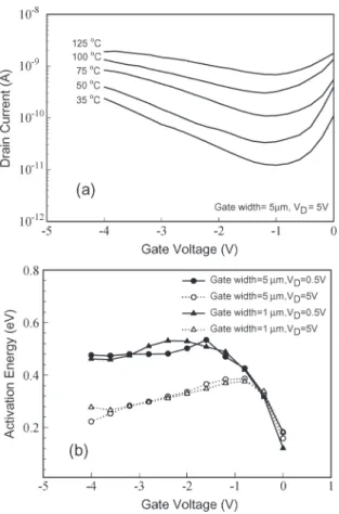
leakage is actually proportional to the gate width. The activation energy for devices with gate widths of 5 and 1 µm is extracted by measuring the I−V characteristics at temperatures ranging from 35◦C to 125◦C. The results are shown in Fig. 16. It can be seen that the activation energy is essentially independent of the gate width at both VD= 0.5 V and VD= 5 V, indicating the same leakage mechanism occurring in the devices.
Fig. 16. (a)OFF-state I−V characteristics of the NW device measured at different temperatures. (b) Activation energy of the NW devices measured at
VD= 0.5 or 5 V as a function of the gate voltage.
From these observations, we conclude that the difference of the OFF-state current among the devices shown in Fig. 15 is mainly dependent on the area of the top gate-to-drain overlap region (or the gate width indicated in Fig. 13, since the edge length of the drain along the channel direction is the same for all NW devices). Gate-induced drain leakage (GIDL) [14] is the most likely cause for the anomalously high OFF-state current. The GIDL current is due to the high field presenting at the oxide/drain region due to high VGD. Such high field tends to deplete the drain and eventually leads to the band-to-band or trap-assisted tunneling process in the region. The origin of the leakage in the NW devices is related to the unique dopant pro-file in the drain. As mentioned in the previous section, the S/D implantation was deliberately performed at a low energy (e.g., 15 keV) to avoid excess dopants being incorporated in the NW channels. This results in a gradient dopant distribution in the drain region, where the dopant concentration decreases toward the oxide/Si interface. This aggravates the GIDL current since it is more vulnerable to depletion by the gate bias in theOFFstate. As indicated in Fig. 16, the activation energy is strongly related to the voltage difference between the gate and the drain or the strength of electric field in the drain near the oxide/Si interface. This could be qualitatively explained as follows.
1) Under low electric-field regime: TheOFF-state current is mainly dominated by thermal emission via the midgap traps located at the grain boundaries. As a consequence, the activation energy is about half of the bandgap.
The use of NWs as the channel of the devices is effective for performance improvement. As demonstrated in this paper, much higher ON-current per unit width as well as steeper subthreshold swing can be achieved using the NW channels. Nevertheless, one potential concern associated with the fabri-cated devices with SPC poly-Si channel is the magnitude of the drive current, since the carrier mobility is seriously degraded by the granular structure. Moreover, the nanoscale channel width would pose a further limitation. The constraints could be relieved by increasing the number of channel in a device with comb-type gate structure and/or by improving the performance with mobility-enhancement techniques, like the excimer laser crystallization (ELC) [15] or metal-induced lateral crystalliza-tion (MILC) [16]. The latter approach has been adopted in one of our studies carried out recently, where the MILC technique was applied to improve the carrier mobility and theON-current, which is to be reported elsewhere [17].
The OFF-state leakage current of the fabricated devices is identified to be due to the GIDL mechanism occurring at the top gate-to-drain overlap region. Major factors are the strength of electric field and the dopant concentration at the drain/oxide interface as well as the trap density in the channel film. Sev-eral strategies could be used to reduce the OFF-state leakage: 1) Reduce the area of top gate-to-drain overlap region [Fig. 12(a)]. 2) Use of plasma treatment to passivate the traps in the channel. This is evidenced by the results shown in Fig. 7. 3) Reduce the trap density in the Si films through crystallinity enhancement techniques, like the ELC or MILC methods. 4) Increase the thickness of dielectric between the drain and gate at the top gate-to-drain overlap region. This is a simple way to reduce the field strength, and it could be easily imple-mented in the device fabrication by simply adding a dielectric hard mask over the top of the gate. 5) Increase the dopant concentration in the drain region near the oxide interface by additional anneal treatments. Note that, such anneal should be done after the NW-etching step to avoid excess incorporation of the dopants into the channel.
V. CONCLUSION
In this paper, we have investigated the performance of TFTs configured with novel poly-Si NW channels formed with SPC method. The fabrication is simple and does not involve costly lithography tools. Such NW structure has been shown to be excellent in terms of ON-current per unit width and the controllability over the short-channel effects. Owing to
Prof. T.-Y. Huang and Prof. Y.-H. Yang for their great support and encouragement.
REFERENCES
[1] F. L. Yang, D. H. Lee, H. Y. Chen, C. Y. Chang, S. D. Liu, and C. C. Huang et al., “5 nm-gate nanowire FinFET,” in VLSI Symp. Tech. Dig., 2004, pp. 196–197.
[2] S. Ecoffey, M. Mazza, V. Pott, D. Bouvet, A. Schmid, and Y. Leblebici
et al., “A new logic based on hybrid MOSFET-polysilicon nanowires,” in IEDM Tech. Dig., Dec. 2005, pp. 277–280.
[3] L. Risch, L. Dreekornfeld, J. Hartwich, F. Hofmann, J. Kretz, and M. Stadele, “Multi gate transistors and memory cells for future CMOS generation,” in Proc. Tech. Dig. IEEE Silicon Nanoelectron. Workshop, 2004, pp. 1–2.
[4] X. Duan, C. Niu, V. Sahi, J. Chen, J. W. Parce, S. Empedocles, and J. L. Goldman, “High-performance thin-film transistors using semiconductor nanowires and nanoribbons,” Nature, vol. 425, no. 6955, pp. 274–278, Sep. 2003.
[5] Y. Cui, Q. Wei, H. Park, and C. M. Lieber, “Nanowire nanosensors for highly sensitive and selective detection of biological and chemical species,” Science, vol. 293, no. 5533, pp. 1289–1292, Aug. 2001. [6] Z. Li, Y. Chen, X. Li, T. I. Kamins, K. Nauka, and R. S. Williams,
“Sequence-specific label-free DNA sensors based on silicon nanowires,”
Nano Lett., vol. 4, no. 2, pp. 245–247, Apr. 2004.
[7] J. E. Jang, S. N. Cha, Y. Choi, T. B. Butler, D. J. Kang, and D. G. Hasko
et al., “Nanoelectromechanical DRAM for ultra-large-scale integration,”
in IEDM Tech. Dig., Dec. 2005, pp. 269–272.
[8] Y. Huang, X. Duan, Q. Wei, and C. M. Lieber, “Directed assembly of one-dimensional nanostructures into functional networks,” Science, vol. 291, no. 5504, pp. 630–633, 2001.
[9] Y. Wu, Y. Cui, L. Huynh, C. J. Barrelet, D. C. Bell, and C. M. Lieber, “Controlled growth and structures of molecular-scale silicon nanowires,”
Nano Lett., vol. 4, no. 3, pp. 433–436, 2004.
[10] H. C. Lin, M. H. Lee, C. J. Su, T. Y. Huang, C. C. Lee, and Y. S. Yang, “A simple and low-cost method to fabricate TFTs with poly-Si nanowire channel,” IEEE Electron Device Lett., vol. 26, no. 9, pp. 643–645, Sep. 2005.
[11] H. Wang, M. Chan, S. Jagar, V. M. C. Poon, M. Qin, and Y. Wang et al., “Super thin-film transistor with SOI CMOS performance formed by a novel grain enhancement method,” IEEE Trans. Electron Devices, vol. 47, no. 8, pp. 1580–1586, Aug. 2000.
[12] W. B. Jackson, N. M. Johnson, C. C. Tsai, I.-W. Wu, A. Chiang, and D. Smith, “Hydrogen diffusion in polycrystalline silicon thin films,” Appl.
Phys. Lett., vol. 61, no. 14, pp. 1670–1672, Oct. 1992.
[13] H. Wang, M. Chan, Y. Wang, and P. K. Ko, “The behavior of narrow-width SOI MOSFETs with MESA isolation,” IEEE Trans. Electron Devices, vol. 47, no. 3, pp. 593–600, Mar. 2000.
[14] T. E. Chang, C. Huang, and T. Wang, “Mechanisms of interface trap-induced drain leakage current in off-state n-MOSFET’s,” IEEE Trans.
Electron Devices, vol. 42, no. 4, pp. 738–743, Apr. 1995.
[15] I. H. Song, C. H. Kim, S. H. Kang, W. J. Nam, and M. K. Han, “A new multi-channel dual-gate poly-Si TFT employing excimer laser annealing recrystallization on pre-patterned a-Si thin film,” in IEDM Tech. Dig., Dec. 2002, pp. 561–564.
[16] S. W. Lee, T. H. Ihn, and S. K. Joo, “Fabrication of high-mobility p-channel poly-Si thin film transistors by self-aligned metal-induced lateral crystallization,” IEEE Electron Device Lett., vol. 17, no. 8, pp. 407–409, Aug. 1996.
[17] C. J. Su, H. C. Lin, and T. Y. Huang, “High performance TFTs with Si nanowire channels fabricated by metal-induced lateral crystallization,”
characterization, reliability of CMOS devices, and novel SOI device technol-ogy. He has authored or coauthored over 100 technical papers in international journals and conferences in the above areas.
Dr. Lin served on the program committee of the International Reliability Physics Symposium (IRPS) in 2001 and 2002. He also served on the program committee of the International Conference on Solid State Devices and Materials (SSDM) in 2005 and 2006.
Ming-Hsien Lee (S’03) was born in Kaohsiung,
Taiwan, R.O.C., in 1973. He received the B.S. degree from the Department of Electronics Engineering, National Chiao-Tung University, Hsinchu, Taiwan, R.O.C., in 1999, where he is currently working to-ward the Ph.D. degree in the Institute of Electronics. His current research interests are in the fabrication of the nanoscale TFTs and the reliability analysis using novel TFT structures.
Shih-Wen Shen was born in I-Lan, Taiwan, R.O.C.,
in 1977. He received the B.S. degree from the Department of Physics, Fu-Jen Catholic University, Taipei, Taiwan, R.O.C., in 2000 and the M.S. degree from the Institute of Electrophysics, National Chiao-Tung University, Hsinchu, Taiwan, R.O.C., in 2002.
He joined the National Nano Device Laboratories (NDL), Taiwan, R.O.C., in 2003, where he is cur-rently an Assistant Researcher. His current research interests are in the nanoscale device technology.