Fabrication of epitaxial ZnO
films by atomic-layer deposition with interrupted flow
Ching-Shun Ku
a, Jheng-Ming Huang
b, Chih-Ming Lin
b,⁎
, Hsin-Yi Lee
a,c,⁎
a
National Synchrotron Radiation Research Center, 101 Hsin-Ann Road, Hsinchu Science Park, Hsinchu 30076, Taiwan
b
Department of Applied Science, National Hsinchu University of Education, Hsinchu 300, Taiwan
cDepartment of Materials Science, National Chiao Tung University, Hsinchu 300, Taiwan
a b s t r a c t
a r t i c l e i n f o
Available online 17 September 2009 Keywords:
ZnO
Atomic layer deposition Flow-rate interruption X-ray diffraction
We formed epitaxial ZnO thinfilms on a (0001) c-plane sapphire substrate through deposition of atomic layers (ALD) at 25–160 °C using diethylzinc (DEZn) and deionized water as precursors in combination with interrupted flow. High-resolution X-ray diffraction measurements were employed to characterize the microstructure of thesefilms. With interrupted flow, we obtained ZnO thin films with an optimal growth window in a range of 40–160 °C, effectively decreasing the growth temperature by about 120 °C relative to a conventional method involving continuousflow. X-ray reflectivity measurements showed that the rate of growth increased also between 20 °C and 120 °C. The XRD results indicate that the stock time might extend the reaction of DEZn and water through an increased duration. All results show that a low temperature for growth improves the crystalline quality and is consistent with thermodynamically blocked self-compensation.
© 2009 Elsevier B.V. All rights reserved.
1. Introduction
Zinc oxide (ZnO) is a material with a remarkably direct and wide band gap (Eg= 3.4 eV near 22 °C) and a large binding energy
∼60 meV[1]. ZnO is a prospective material for several applications, such as light-emitting diodes (LED),field-effect transistors (FET), UV lasers near 300 K, gas sensors, piezoelectric transducers, transparent electronics, surface-acoustic-wave devices, solar cells, and spintronics, when doped with transition-metal elements[2–9]. Thinfilms of ZnO are grown with various techniques such as a sol–gel method[10], radio-frequency magnetron sputtering[11,12], pulsed laser deposition [13,14], oxidation of zinc-based materials [15,16], metallorganic chemical-vapor deposition (MOCVD)[17,18], molecular-beam epitaxy (MBE)[19,20]or atomic-layer deposition (ALD)[21–24]. An indis-pensable requisite for an application in optoelectronics is doping of ZnO with both n- and p-types. From the energy gap about 3.4 eV, one can calculate an intrinsic concentration of free carriers at a level 106cm− 3, which is a magnitude 10− 11–10− 15times those reported
for zinc-oxide layers grown by various methods. The great extent of electron doping in nominally undoped ZnO is attributed to zinc interstitials, oxygen vacancies and hydrogen[25]. Deposition at high temperature can intensify the formation of oxygen vacancies, to contribute to the high level of n-electron doping. This point has been little explorsed because effort was concentrated on obtaining ZnO films of great structural quality, which requires a high temperature
for growth. Incorporated carbonates and hydrogen carbonates might also contribute to the n-type conductivity of ZnOfilms as grown[26]; these defects, producing heavy n-type doping, introduce shallow donor levels approximately 0.01–0.05 eV below the minimum of the conduc-tion band of ZnO[27–29].
The growth of ZnO at a low temperature is crucial to avoid foreign phases in a material doped with a transition metal[30], but the most densely packed and thermodynamically favorable growth orientation in wurtzite structures has the c-axis perpendicular to a substrate. ZnOfilms with the c-axis normal to the substrate are thus generally preferable, but we show that the c-axis is parallel to a direction normal to the substrate when growth occurs at a low temperature. Moreover, such growth makes possible the obtaining of ZnO onflexible or organic substrates. The exact value of the concentration of free carriers in a ZnO thinfilm depends strongly on the method of, and parameters during, growth. The most important factor to influence the electric parameters of a ZnO thin film is the growth temperature, because it controls the thermodynamics of that growth[31]. In this work, we report the use of a novel adaptation of ALD with an interruptedflow that enables us to obtain epitaxial ZnOfilms of high quality near 22 °C.
2. Experimental
ALD involves a self-limiting vapor-phase chemisorption that relies on consecutive surface reactions and utilizes critical purge steps to prevent interactions between reactive precursors[29]. All processes occur with sustained pumping to evacuate superfluous reactants; this method is also called‘continuous-flow’ ALD. Although ALD is superior in a particular temperature range to other methods of deposition, the temperature is also an important parameter to control the preferred
Thin Solid Films 518 (2009) 1373–1376
⁎ Corresponding authors. Lee is to be contacted at National Synchrotron Radiation Research Center, 101 Hsin-Ann Road, Hsinchu Science Park, Hsinchu 30076, Taiwan. Tel.: +886 3 5780281x7120; fax: +886 3 5783813.
E-mail addresses:[email protected](C.-M. Lin),[email protected]
(H.-Y. Lee).
0040-6090/$– see front matter © 2009 Elsevier B.V. All rights reserved. doi:10.1016/j.tsf.2009.09.018
Contents lists available atScienceDirect
Thin Solid Films
orientation of a deposited thinfilm[30], but at a very low temperature the growth rate decreases and a conformal monolayer is not deposited because the thermal budget is insufficient. In this work, we introduce another ALD that we call a‘flow-rate interruption’ method (FIM). We installed a quick ALD diaphragm valve (Swagelok) between the reactor and the pump station. To retain the precursor in the reactor chamber, this valve is closed before the precursor is introduced into the reactor. The main influence of this step is to enhance the precursor density in the reactor and to extend the duration of reaction between the reactant and the sample surface. These two effects might increase the rate of reaction at a low temperature. The interval during which the reactant is held in the reaction chamber is called a stock time. We
deposited ZnO films on (0001) sapphire substrates using ALD at temperatures in a range of 25–200 °C. The pulse durations of water, 15 ms, and DEZn, 10 ms, precursors were the same for both growth modes; the stock time was 3 s for both water and DEZn in the stock mode. All other conditions for both modes and precursors were the same. The purge and pumping periods were 10 s and 6 s respectively; the purge gas was N2and the pressure was set to 2 Torr. All samples
were obtained with growth during 200 ALD cycles, with a total thickness about 50–80 nm for the varied growth temperature.
X-ray diffraction (XRD) measurements at high resolution were conducted at wiggler beamline BL-17B1 in the National Synchrotron Radiation Research Center (NSRRC), Hsinchu, Taiwan. Using two pairs of slits between the sample and the detector produced a typical wave-vector resolution∼0.001 nm− 1in the vertical scattering plane
in this experiment.
Photoluminescence (PL) measurements were performed on samples at 295 K using He–Cd laser (325 nm, IK3252R-E, Kimmon) for excitation and a CCD (80 K, Spec-10, Princeton Instruments) with a monochromator (0.5 m, SP-2558A, Acton) for detection. The effective resolution of the PL spectrum was 0.02 nm.
3. Results and discussion
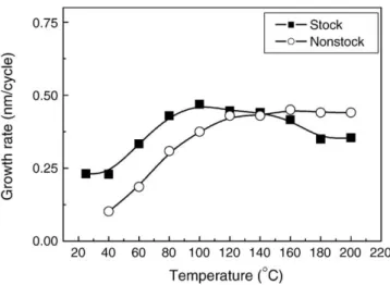
The rate of deposition calculated from the X-ray reflectivity results is shown inFig. 1. The growth rate increases on applying a stock time for growth in the temperature range of 40 °C to 100 °C. Aflat region of growth rate with temperature from 120 °C to 200 °C is seen for the non-stock mode. For a temperature less than 120 °C in the non-stock mode, the growth rate decreased linearly proportionally to temper-ature. There is no oscillation fringe in the X-ray reflectivity curve at 25 °C for the non-stock mode, which indicates no growth of a ZnO thinfilm on sapphire at such a temperature. In contrast, for the stock mode not only was the growth curve extended from 120 °C to 80 °C but also the curve slightly slants from 100 °C to 200 °C. Moreover, the growth rate was enhanced even from 25 °C to 100 °C in contrast with the non-stock mode.
We examined the structural properties of the thinfilm using an X-ray radial scan (θ–2θ) along the surface normal of ZnO samples; the results inFig. 2display only a ZnO (002) reflection peak located at∼2.42 Å− 1of the non-stock mode for a growth temperature less
than 100 °C, and a (101) peak appeared when the growth temper-ature was increased beyond 100 °C. In contrast, the ZnOfilm deve-loped in the stock mode not only had an enhanced (002) peak but also suppressed the (101) phase until growth temperature increased
Fig. 1. Rate of growth at varied temperature in stock and non-stock modes.
Fig. 2. X-ray normal scan along the ZnO (002) reflection peak with varied growth temperature in stock and non-stock modes.
Fig. 3. Variation with temperature of the ratio of the ZnO (002) integrated intensity between stock and non-stock modes; the inset shows the original intensity in the stock and non-stock modes.
beyond 180 °C. This effect might be attributed to the stock time extending the reaction period of DEZn and water to perform a conformal monolayer, and a small thermal budget forced also the crystal orientation to become well aligned with the surface normal to decrease the surface energy at growth temperature∼180 °C. For the highest growth temperature, 200 °C, the long processing duration not only caused surface desorption of precursors to decrease the growth rate as shown inFig. 1but also destroyed the arrangement of surface atoms because of abundant thermal energy that induces surfacefluctuation, resulting in a decreased XRD peak intensity.
Fig. 3shows the integrated intensity ratio of the (002) reflection between the stock mode and the non-stock mode; the inset shows the original intensity of both modes. The intensity of the ZnO (002) diffraction peak for a sample grown in the non-stock mode remained almost constant throughout the entire range of growth temperature. In addition, the stock-type ZnO film results indicated a greatly increased intensity for a growth temperature less than 100 °C; the intensity for the stock mode was almost 16 times that of the non-stock mode at 40 °C. For the stock mode the full width at half maximum (FWHM) of the (002) diffraction peak also diminished relative to the non-stock mode. These results indicate that the stock time added for growth substantially improves the crystal quality of the thinfilm and appreciably enlarges the growth window. We estimated the grain
size of ZnO thinfilms based on XRD results as shown inFig. 2and Scherrer's formula,
D = Kλ
Δð2θÞcosθ ð1Þ
in which K = 180/π̣ and λ̣ is the X-ray wavelength (λ=0.15495 nm for 8-keV synchrotron X-rays). The results for thefilms appear in Fig. 4. The grain size in the stock mode is approximately∼50 nm, near the total thickness of the ZnOfilms. This evidence likely explains how the stock mode suppresses the (101) phase through the region of a single domain from the interface to thefilm surface. The decreased grain size at the highest growth temperature, 200 °C, with the stock mode might be due to surface desorption breaking the crystal stacking and developing the grain boundaries. A XRD scan in the normal direction showed that the ZnO c⇀-axis was satisfactorily aligned with
the sample surface. We inspected the off-normal scan to examine the epitaxial relation between thefilm and the substrate. The distri-bution of X-ray intensity of an off-normal radial scan for a ZnOfilm deposited at 40 °C is shown inFig. 5, which shows a sapphire (113) scan along the Miller index of reciprocal lattice space, and the x-axis in the H index of reciprocal lattice units (r. l. u.) referred to the sapphire substrate. A broad feature coexists with a narrow Bragg line, which originates from the sapphire substrate; this broad feature, indicated by arrows inFig. 5, is ascribed to the ZnO (101) Bragg signal of the deposited layer. Azimuthal scans of a depositedfilm near a ZnO (101) surface signal and the sapphire (113) substrate Bragg signal, as shown in the inset ofFig. 5, clearly exhibit six-fold symmetry and have nearly the same intensity. No other feature was observed in the intervals between the six peaks, indicating an effective alignment of a
⇀
and b⇀axes of ZnO unit cells along those of the sapphire substrate. These results constitutefirm evidence for a strongly epitaxial layer
Fig. 4. Distribution of grain size for ZnO thinfilms with varied growth temperature.
Fig. 5. Off-normal radial scan along the sapphire [113] direction observed in the stock mode with growth temperature 40 °C. The inset shows a comparison ofϕ-scan between
sapphire (113) and ZnO (101). Fig. 6. Photoluminescence results in the stock and non-stock mode for samples at 22 °C. 1375 C.-S. Ku et al. / Thin Solid Films 518 (2009) 1373–1376
deposited on the substrate. This evidence is thefirst that epitaxial ZnOfilms have been formed on a (0001) c-plane sapphire substrate in the ALD region with an FRI method for growth in a temperature range of 25–160 °C.
PL spectra show a strong near-band-edge (NBE) excitonic emission near 22 °C for all investigated ZnOfilms deposited with DEZn pre-cursors.Fig. 6shows that in the stock mode the PL intensity much increased for a growth temperature from 60 °C to 180 °C relative to a non-stock mode. The integrated intensity increased from 25 °C and attained a maximum at 100 °C for the stock mode about seven times that of the non-stock mode. PL spectra for both stock and non-stock modes showed no significant other defect-related emission band, even though the CCD has significant quantum efficiency in this region. Furthermore, the PL intensity increased at growth temperatures of 60–180 °C, but XRD results show a diffraction peak enhanced from 40 °C to 120 °C. Combining the PL and XRD results, we deduced that growth of a ZnO thinfilm with ALD and FRI is optimum at 60–120 °C. 4. Conclusion
Thin crystallinefilms of zinc oxide (ZnO) of high quality have been grown epitaxially on a (0001) c-plane of a sapphire substrate by ALD technique in a temperature range of 25–160 °C with an interrupted flow. The XRD results indicate that the stock time might improve the reaction chain of DEZn and water through an enhanced duration of reaction and an enhanced rate of reaction at an increased pressure in the chamber. The PL results exhibit that a strong exciton emission, enhanced because of a small thermal energy, might obstruct self-compensation processes between Zn and O to diminish the defect density of ZnO thinfilms. The low temperature for growth results in increased crystalline quality and enhanced optical properties of ZnO films.
Acknowledgement
The National Science Council of the Republic of China, Taiwan, provided support under contract NSC 2221-E-213-001, NSC 97-2112-M-134-001-MY2 and NSC 97-2120-M-001-007.
References
[1] A. Mang, K. Reimann, S. Rubenacke, Solid State Commun. 94 (1995) 251. [2] S.J. Pearton, D.P. Norton, K. Ip, Y.W. Heo, T. Steiner, Superlattices Microstruct. 34
(2003) 3.
[3] Ü. Özgür, Ya.I. Alivov, C. Liu, A. Teke, M. Reshchikov, S. Dogan, V. Avrutin, S.-J. Cho, H. Morkoc, J. Appl. Phys. 98 (2005) 041301.
[4] D.C. Reynolds, D.C. Look, B. Jogai, Solid State Commun. 99 (1996) 873. [5] M. Wraback, H. Shen, S. Liang, C.R. Gorla, Y. Lu, Appl. Phys. Lett. 74 (1999) 507. [6] D.C. Look, D.C. Reynolds, J.W. Hemsky, R.L. Jones, J.R. Sizelove, Appl. Phys. Lett. 75
(1999) 811.
[7] W.Z. Xu, Z.Z. Ye, Y.J. Zeng, L.P. Zhu, B.H. Zhao, L. Jiang, J.G. Lu, H.P. He, S.B. Zhang, Appl. Phys. Lett. 88 (2006) 173506.
[8] P.F. Carcia, R.S. McLean, M.H. Reilly, Appl. Phys. Lett. 88 (2006) 123509. [9] Z.K. Tang, G.K.L. Wong, P. Yu, M. Kawasaki, A. Ohtomo, H. Koinuma, Y. Segawa,
Appl. Phys. Lett. 72 (1998) 3270.
[10] S. O'Brien, L.H.K. Koh, G.M. Crean, Thin Solid Films 516 (2008) 1391.
[11] T. Hiramatsu, M. Furuta, H. Furuta, T. Matsuda, T. Hirao, Jpn. J. Appl. Phys. 46 (2007) 3319 Part 1.
[12] L. Jianguo, Z. Yinzhu, Y. Zhizhen, W. Lei, Z. Binghui, H. Jinhyun, Mater. Lett. 57 (2003) 3311.
[13] S.M. Park, T. Ikegami, K. Ebihara, Thin Solid Films 513 (2006) 90.
[14] Z.K. Tang, G.K.L. Wong, P. Yu, M. Kawasaki, A. Ohtomo, H. Koinuma, Y. Segawa, Appl. Phys. Lett. 72 (1998) 3270.
[15] E. Kaminska, A. Piotrowska, J. Kossut, A. Barcz, R. Butkute, W. Dobrowski, E. Dynowska, R. Jakiela, E. Przezdziecka, R. Lukasiewicz, M. Aleszkiewicz, P. Wojnar, E. Kowalczyk, Solid State Commun. 135 (2005) 11.
[16] E. Przezdziecka, E. Kaminska, I. Pasternak, A. Piotrowska, J. Kossut, Phys. Rev. B 76 (2007) 193303.
[17] B.P. Zhang, K. Wakatsuki, N.T. Binh, N. Usami, Y. Segawa, Thin Solid Films 449 (2004) 12.
[18] L. Xiaonan, S.E. Asher, S. Limpijumnong, B.M. Keyes, C.L. Perkins, T.M. Barnes, H.R. Moutinho, J.M. Luther, S.B. Zhang, H.S. Wei, T.J. Coutts, J. Cryst. Growth 287 (2006) 94.
[19] D.C. Look, D.C. Reynolds, C.W. Litton, R.L. Jones, D.B. Eason, G. Cantwell, Appl. Phys. Lett. 81 (2002) 1830.
[20] F.X. Xiu, Z. Yang, L.J. Mandalapu, D.T. Zhao, J.L. Liu, W.P. Beyermann, Appl. Phys. Lett. 87 (2005) 152101.
[21] A. Wojcik, M. Godlewski, E. Guziewicz, R. Minikayev, W. Paszkowicz, J. Cryst. Growth 310 (2008) 284.
[22] J. Lim, C. Lee, Thin Solid Films 515 (2007) 3335. [23] J. Lim, K. Shin, H.W. Kim, C. Lee, J. Lumin. 109 (2004) 181.
[24] S.K. Kim, C.S. Hwang, S.-H.K. Park, S.J. Yun, Thin Solid Films 478 (2005) 103. [25] F. Oba, S.R. Nishitani, S. Isotani, H. Adachi, J. Appl. Phys. 90 (2001) 824. [26] K.G. Saw, K. Ibrahim, Y.T. Lim, M.K. Chai, Thin Solid Films 515 (2007) 2879. [27] S.J. Pearton, D.P. Norton, K. Ip, Y.W. Heo, T. Steiner, Superlattices Microstruct.
34 (2003) 3.
[28] Ü. Özgür, Ya.I. Alivov, C. Liu, A. Teke, M. Reshchikov, S. Dogan, V. Avrutin, S.-J. Cho, H. Morkoc, J. Appl. Phys. 98 (2005) 041301.
[29] P.F. Carcia, R.S. McLean, M.H. Reilly, Appl. Phys. Lett. 88 (2006) 123509. [30] A. Wojcik, M. Godlewski, E. Guziewicz, K. Kopalko, R. Jakiela, M. Kiecana, M. Sawicki,
M. Guziewicz, M. Putkonen, L. Niinisto, Y. Dumont, N. Keller, Appl. Phys. Lett. 90 (2007) 082502.
[31] C.G. Van der Walle, R.A. Street, Phys. Rev., B 51 (1995) 10615. 1376 C.-S. Ku et al. / Thin Solid Films 518 (2009) 1373–1376