Field emission from aligned carbon nanofibers grown in situ by hot filament chemical
vapor deposition
Chia-Fu Chen, Chien-Liang Lin, and Chi-Ming Wang
Citation: Applied Physics Letters 82, 2515 (2003); doi: 10.1063/1.1568163 View online: http://dx.doi.org/10.1063/1.1568163
View Table of Contents: http://scitation.aip.org/content/aip/journal/apl/82/15?ver=pdfcov Published by the AIP Publishing
Articles you may be interested in
Effects of a nanocomposite carbon buffer layer on the field emission properties of multiwall carbon nanotubes and nanofibers grown by hot filament chemical vapor deposition
J. Vac. Sci. Technol. B 24, 639 (2006); 10.1116/1.2174026
Electron field emission from room temperature grown carbon nanofibers J. Appl. Phys. 95, 3153 (2004); 10.1063/1.1647261
Field emission from aligned carbon nanotubes prepared by thermal chemical vapor deposition of Fe-phthalocyanine
Appl. Phys. Lett. 79, 2636 (2001); 10.1063/1.1410874
Fabrication of gated cathode structures using an in situ grown vertically aligned carbon nanofiber as a field emission element
J. Vac. Sci. Technol. B 19, 573 (2001); 10.1116/1.1358855
In situ-grown carbon nanotube array with excellent field emission characteristics Appl. Phys. Lett. 76, 3813 (2000); 10.1063/1.126790
This article is copyrighted as indicated in the article. Reuse of AIP content is subject to the terms at: http://scitation.aip.org/termsconditions. Downloaded to IP: 140.113.38.11 On: Wed, 30 Apr 2014 08:39:25
Field emission from aligned carbon nanofibers grown
in situ
by hot
filament chemical vapor deposition
Chia-Fu Chen, Chien-Liang Lin,a)and Chi-Ming Wang
Department of Materials Science and Engineering, National Chiao Tung University, 1001 Ta Hsueh Road, Hsinchu 30049, Taiwan, Republic of China
共Received 14 November 2002; accepted 18 February 2003兲
Aligned high-aspect-ratio carbon nanofibers were grown in situ using modified hot filament chemical vapor deposition. The field-emission properties were then studied. An Fe–Cr wire filament acted as a catalytic source and a heat source. Carbon nanofibers were deposited on a Si substrate with CO2 as a carrier gas through ethanol. The experimental results indicate that the flow in the horizontal direction to the substrate produces carbon nanofibers with diameters of less than 10 nm. The field-emission current of 2 V/m was 0.54 mA/cm2; the turn-on field of the sample was 1.1 V/m. © 2003 American Institute of Physics. 关DOI: 10.1063/1.1568163兴
Field-emission display is evolving as a promising tech-nique for manufacturing the next generation of flat panel displays共FPD兲. Indeed, much effort has been made to make metal-tip emitters and silicon-tip array field-emission devices.1However, the electrical field required to trigger the field emission of such devices is quite high. Moreover, their performance rapidly deteriorates due to thermal effects, caus-ing serious contamination and damage to the emitter materi-als. A good candidate for field emitters must have a high-aspect-ratio structure, low work function, and stable chemistry properties. For applications such as FPDs, large-area films of nanotubes,2,3 or nanofibers,4,5 which produce uniform field emissions across the surface are required. Dense aligned fibers normal to the substrate can further en-hance the field emission and the uniformity of such emission. Recently, Chen et al.6grew aligned graphitic nanofibers on single crystalline Ni共100兲 substrate by plasma-assisted hot filament chemical vapor deposition 共HFCVD兲 using a gas-eous mixture of nitrogen and methane. Small Ni particles generated by the plasma on the surface of the substrate cata-lyzed the growth of nanofibers with diameters of 100–200 nm and a density of 108/cm2. The method was extended to synthesize thinner aligned graphitic nanofibers with greater packing density by modifying the deposition process.4 How-ever, the thinnest nanofibers they obtained were 30 nm. Our recent study reported a simple, nontoxic, inexpensive in situ HFCVD method for preparing multiwalled nanotubes on silicon.7 The method uses a filament as the heat source for pyrolysis and catalytic evaporation of the Fe–Cr filament. In this study, using our method, nanotubes and nanofibers were deposited when the carrier gas flowed vertically and horizon-tally to the substrate, respectively. Thinner nanofibers were developed and applied in field emission.
Our earlier report described the simplified chemical va-por deposition 共CVD兲 method for synthesizing carbon nanotubes.7 The apparatus used for synthesis is similar to that used to deposit CVD diamond. However, tungsten is the filament material most commonly used in diamond deposi-tion. Here, an Fe–Cr wire is coiled as a filament to grow
nanotubes and nanofibers. Such an Fe–Cr wire is frequently used in furnace heating. The wire is not high grade and has several impurities, being composed of Fe 共72.43%兲, Cr
共23.42%兲, Mn 共3.45%兲, and Ni 共0.69%兲. Deposition needed
not be in vacuo, and process pressure was closed to the at-mosphere. Carbon nanotubes and nanofibers were deposited on the Si substrate with CO2 as a carrier gas that passed through ethanol. Different directions of flow of CO2 onto the substrate were adopted to confirm the effect of deposition conditions by adjusting the position of the gas inlet nozzle. The system used a 1 mm diameter Fe–Cr wire, and was heated by an ac current of 22 A at 40 V. In this experiment, the temperature of the filament was approximately 1200 °C, which was 100–200 °C lower than its melting point. The distance of the filament to the sample was 2 mm. The growth proceeded for 15 min.
After deposition, each sample was first visually exam-ined. The surface of the sample near the bottom of the coiled filament was the blackest. The location of the nanofibers on the sample was examined using a scanning electron micro-scope 共SEM兲. The images reveal that most nanofibers were near the bottom of the coiled filament. Figure 1共a兲 displays the SEM image of these nanofibers. These nanofibers were produced when CO2 carrier gas flowed horizontally to the substrate. Bundles of nanofibers are observed on the center of the substrate. The nanofibers have a high-aspect ratio, im-plying good field-emission characteristics. Figure 1共b兲 shows SEM image of nanotubes obtained using CO2 carrier gas which flowed vertically toward the substrate. A fixed CO2 flow rate of 15 sccm yielded two completely different mor-phologies. Figure 1共b兲 shows a random tube network that consists of numerous curved tubes was formed; the tubes are 50–70 nm in diameter and a few tens of microns long. We supposed that flow direction should change the distribution and particle size of catalysts which originated from a fila-ment on the silicon sample.
The carbon nanofiber in Fig. 2, referred to in Fig. 1共a兲, is clearly solid in contrast to the hollow structure of the carbon nanotube. The insertion in Fig. 2 displays a transmission electron microscope 共TEM兲 image of an end section of an individual nanofiber. The structure is similar to that of a car-a兲Electronic mail: [email protected]
APPLIED PHYSICS LETTERS VOLUME 82, NUMBER 15 14 APRIL 2003
2515
0003-6951/2003/82(15)/2515/3/$20.00 © 2003 American Institute of Physics
This article is copyrighted as indicated in the article. Reuse of AIP content is subject to the terms at: http://scitation.aip.org/termsconditions. Downloaded to IP: 140.113.38.11 On: Wed, 30 Apr 2014 08:39:25
bon fiber, but with a nanosized diameter. Under both growth conditions, the temperature of samples was almost the same
共⬃700 °C兲. Therefore, carbon nanofibers with a diameter of
10 nm can be grown using this HFCVD method by simply
adjusting the direction of flow of the carrier gas. The diam-eters of the fibers are smaller than those obtained in other reports which mostly include diameters of 30–100 nm.4
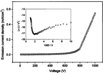
Figure 3 displays the electron-emitting characteristics of the nanofibers obtained using a diode structure. An anode, indium tin oxide glass, was separated by 500 m from the tip of the cathode made of nanofibers. The current–voltage properties were measured using an electrometer 共Keithley 237兲 and analyzed through the Fowler–Nordheim 共F–N兲 model. The emission current at an applied voltage of 1000 V was 0.54 mA/cm2. The macroscopic turn-on field, which is the field needed to extract a current density of 10 A/cm2, was 1.1 V/m. One report8 concluded that a comparison among film field emitters is pertinent only if the field-emission measurements, especially the interelectrode dis-tance and geometry, were taken under the same experimental conditions. However, the field enhancement factor, , is to be extracted using a commonly used method.
In 1928, Fowler and Nordheim proposed the model of field emission from a solid.9The F–N model states that the relationship between the emitted current in the local electric field F and the work function is I⬀ (F2/)exp(B3/2/F), with B⫽6.83⫻109共VeV⫺3/2m⫺1兲. The local electric field F is not simply V/d, which is the macroscopic field obtained with an applied voltage V between two electrodes separated by a distance d. Rather, F is, in most cases, larger by an enhancement factor, which reflects the ability of the emit-ter to amplify the field. is determined mostly by the geo-metrical shape of the emitter, and the field at the emitter surface is frequently expressed as F⫽E⫽V/d, where E ⫽V/d is the macroscopic field. Moreover, literature includes
arguments based on values of that have been determined from the shape of the emitter, and especially from its radius of curvature at the tip, Rtip. The most basic approximation is
F⬇V/(k•Rtip), where k is a constant that depends on the geometry and is taken to be equal to 5 for an infinitely long cylindrical emitter.10From the aforementioned definition and approximation for F, ⫽d/(k•Rtip) is obtained. Thus, Rtip
⫽10 nm yields ⫽10 000.
In summary, a modified HFCVD method is reported for synthesizing in situ carbon nanofibers, using CO2as a carrier gas through ethanol. Nanotubes and nanofibers were depos-ited when the carrier gas flowed vertically and horizontally FIG. 1. SEM images of two carbon nanostructures on silicon samples.共a兲
Nanofibers are obtained with CO2carrier gas that flows horizontally and共b兲 nanotubes are obtained with CO2carrier gas that flows vertically.
FIG. 2. TEM images of nanofiber, obtained with CO2carrier gas that flows horizontally.
FIG. 3. Emission current density against applied voltage and the F–N plot for the nanofibers, obtained with CO2carrier gas that flows horizontally.
2516 Appl. Phys. Lett., Vol. 82, No. 15, 14 April 2003 Chen, Lin, and Wang
This article is copyrighted as indicated in the article. Reuse of AIP content is subject to the terms at: http://scitation.aip.org/termsconditions. Downloaded to IP: 140.113.38.11 On: Wed, 30 Apr 2014 08:39:25
to the substrate, respectively. However, this study demon-strates that the uniformity of the nanofibers grown on the sample must be further improved, especially with respect to filament configuration since the sample surface near the bot-tom of the coiled filament was blackest, and revealed that most nanofibers were grown here. Aligned carbon nanofibers with diameters of less than 10 nm were formed, and related field-emission properties were measured. In the experiment, the carbon nanofibers showed field-emission characteristics that included a turn-on field of 1.1 V/m and an emission current of 0.54 mA at 2 V/m.
The authors would like to thank the National Science Council of the Republic of China, Taiwan for financially sup-porting this work under Contract No. NSC 91-2219-E-009-029.
1C. A. Spindt, I. Brodie, L. Humphrey, and E. R. Westberg, J. Appl. Phys.
47, 5248共1976兲.
2M. Hirakawa, S. Sonoda, C. Tanaka, H. Murakami, and H. Yamakawa, Appl. Surf. Sci. 169, 662共2001兲.
3O. M. Ku¨ttel, O. Groening, C. Emmenegger, and L. Schlapbach, Appl. Phys. Lett. 73, 2113共1998兲.
4Y. Chen, S. Patel, Y. Ye, D. T. Shaw, and L. Guo, Appl. Phys. Lett. 73, 2119共1998兲.
5M. A. Guillorn, A. V. Melechko, V. I. Merkulov, E. D. Ellis, C. L. Britton, M. L. Simpson, D. H. Lowndes, and L. R. Baylor, Appl. Phys. Lett. 79, 3506共2001兲.
6
Y. Chen, Z. L. Wang, J. S. Yin, D. J. Johnson, and R. H. Prince, Chem. Phys. Lett. 272, 178共1997兲.
7
C. F. Chen, C. L. Lin, and C. M. Wang, Jpn. J. Appl. Phys., Part 2 41, L67
共2002兲.
8
J. M. Bonard, M. Croci, I. Arfaoui, O. Noury, D. Sarangi, and A. Chaˆt-elain, Diamond Relat. Mater. 11, 763共2002兲.
9R. H. Fowler and L. W. Nordheim, Proc. R. Soc. London, Ser. A 119, 173
共1928兲.
10W. P. Dyke and W. W. Dolan, Adv. Electron. Electron Phys. 8, 89共1956兲.
2517
Appl. Phys. Lett., Vol. 82, No. 15, 14 April 2003 Chen, Lin, and Wang
This article is copyrighted as indicated in the article. Reuse of AIP content is subject to the terms at: http://scitation.aip.org/termsconditions. Downloaded to IP: 140.113.38.11 On: Wed, 30 Apr 2014 08:39:25