Formation of silicon germanium nitride layer with distributed charge storage elements
Chun-Hao Tu, Ting-Chang Chang, Po-Tsun Liu, Hsin-Chou Liu, Wei-Ren Chen, Chia-Chou Tsai, Li-Ting Chang, and Chun-Yen Chang
Citation: Applied Physics Letters 88, 112105 (2006); doi: 10.1063/1.2178868 View online: http://dx.doi.org/10.1063/1.2178868
View Table of Contents: http://scitation.aip.org/content/aip/journal/apl/88/11?ver=pdfcov
Published by the AIP Publishing
Articles you may be interested in
Polycrystalline silicon-germanium heating layer for phase-change memory applications
Appl. Phys. Lett. 89, 053517 (2006); 10.1063/1.2335363
Formation of germanium nanocrystals embedded in silicon-oxygen-nitride layer
Appl. Phys. Lett. 89, 052112 (2006); 10.1063/1.2227059
Solid phase epitaxy during Ge condensation from amorphous SiGe layer on silicon-on-insulator substrate
Appl. Phys. Lett. 89, 032101 (2006); 10.1063/1.2222343
On the formation mechanism of epitaxial Ge islands on partially relaxed SiGe buffer layers
J. Vac. Sci. Technol. B 22, 2257 (2004); 10.1116/1.1775188
Effect of germanium concentration and tunnel oxide thickness on nanocrystal formation and charge storage/retention characteristics of a trilayer memory structure
Appl. Phys. Lett. 83, 3558 (2003); 10.1063/1.1615840
This article is copyrighted as indicated in the article. Reuse of AIP content is subject to the terms at: http://scitation.aip.org/termsconditions. Downloaded to IP: 140.113.38.11 On: Thu, 01 May 2014 02:05:51
Formation of silicon germanium nitride layer with distributed charge
storage elements
Chun-Hao Tu
Institute of Electronics, National Chiao Tung University, Hsin-Chu, Taiwan, Republic of China
Ting-Chang Chang
Department of Physics and Institute of Electro-Optical Engineering, National Sun Yat-Sen University, Taiwan, Republic of China and Center for Nanoscience, Nanotechnology, National Sun Yat-Sen University, Taiwan, Republic of China
Po-Tsun Liu
Department of Photonics and Display Institute, National Chiao Tung University, Taiwan, Republic of China
Hsin-Chou Liu, Wei-Ren Chen, Chia-Chou Tsai, Li-Ting Chang, and Chun-Yen Chang
Institute of Electronics, National Chiao Tung University, Hsin-Chu, Taiwan, Republic of China
共Received 28 October 2005; accepted 15 January 2006; published online 15 March 2006兲
The formation of silicon germanium nitride 共SiGeN兲 with distributed charge storage elements is proposed in this work. A large memory window is observed due to the retainable dangling bonds inside the SiGeN gate stack layer. The nonvolatile memory device with the high-temperature oxidized SiGeN stack layer exhibits 2 V threshold voltage shift under 7 V write operation, which is sufficient for a memory device to define the signal “0” and “1.” Also, the manufacture technology using the sequent high-temperature oxidation of the a-Si layer acting as the blocking oxide is proposed to enhance the performance of nonvolatile memory devices. © 2006 American Institute of
Physics. 关DOI:10.1063/1.2178868兴
In the past few years, the portable electronic devices have significantly impacted the market of consumer electron-ics. Because of the low working voltage and nonvolatility, the selection of storage media for most portable electronic devices is the Flash memory which almost bases on the structure of the continuous floating gate 共FG兲.1,2 Despite a huge success in commercializing, conventional FG devices have some drawbacks.2The most prominent one is that once there is a charge leakage path共resulting from P/E-cycle deg-radation兲 in gate oxide, all the charges stored in the floating gate will leak away from this one single path because charges are stored in continuous energy level 共conduction band兲 in FG. The scaling limitation stems from the extreme requirements put on the tunnel oxide layer.3–5To overcome the scaling limits of the conventional FG structure, the SONOS 共historically MNOS兲, or floating-trap structure has drawn much attention recently.6An advantage of the SONOS device over the floating-gate device is its improved endur-ance, since a single defect will not cause the discharge of the memory due to the distributed energy levels which charges store in.7,8The charge storage element of the SONOS struc-ture is an insulating layer of silicon nitride with many dis-crete intrinsic traps共or energy levels兲. Therefore, the triple-dielectric SONOS structure 共poly-Si gate/blocking oxide/ silicon nitride/tunnel oxide/silicon substrate兲 is a potential candidate for high density EEPROM’s and not only suitable for semiconductor manufacture but also a substitution to high-density DRAMs. Recently, different charge storage elements instead of silicon nitride have been studied to achieve the robust distributed charge storage.9–11 In this contribution, the nitride-incorporated silicon germanium 共SiGeN兲 was investigated to be a three novel distributed charge storage element. The charge-trapping layer of SiGeN, fabricated by the directly depositing using plasma enhanced
chemical vapor deposition共PECVD兲 system, exhibits obvi-ous charge-trapping memory effects under electrical mea-surements. Also, material analyses such as Fourier transform infrared spectroscopy共FTIR兲 were utilized to determine the composition of the SiGeN film.
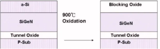
Figure 1 exhibits the process flow in this work. First, a 5 nm thick thermal oxide was grown as the tunnel oxide on
p-type Si substrate by dry oxidation in an atmospheric
pres-sure chemical vapor deposition 共APCVD兲 furnace. Subse-quently, a 20 nm amorphous silicon germanium nitride layer was deposited by plasma enhanced chemical vapor deposi-tion共PECVD兲 on the tunnel oxide, followed by deposition of 20 nm amorphous silicon. The oxidation process was per-formed to fabricate the oxygen-incorporated SiO2 served as blocking oxide, and the oxidation temperature was 900 ° C. Afterward, a steam densification at 900 䊐 was also per-formed for 180 s to densify the blocking oxide. The deposi-tion of the SiGeN film was kept at 200䊐 in a low pressure of 0.6 mTorr with precursors of SiH4 共20 sccm兲, GeH4
共5 sccm兲,NH3 共30 sccm兲, and N2 共500 sccm兲 and plasma
power of 20 W. The low pressure of 0.6 mTorr during depo-sition leads the mean free path of electrons to be increased and to improve the uniformity of the thin film.12The depo-sition conditions of a-Si film, such as temperature and pres-sure, were the same as that of the SiGeN film deposition.
FIG. 1. The process flow proposed in this work.
APPLIED PHYSICS LETTERS 88, 112105共2006兲
0003-6951/2006/88共11兲/112105/2/$23.00 88, 112105-1 © 2006 American Institute of Physics
This article is copyrighted as indicated in the article. Reuse of AIP content is subject to the terms at: http://scitation.aip.org/termsconditions. Downloaded to IP: 140.113.38.11 On: Thu, 01 May 2014 02:05:51
Next, the high temperature a-Si oxidation was performed in the thermal furnace in oxygen ambient. The sequent steam oxidation was performed to improve the quality of oxidized a-Si layer as the blocking oxide. Finally, the Al gate was patterned and sintered to form a metal-oxide-insulator-oxide-silicon共MOIOS兲 structure with the charge trapping insulator of SiGeN.
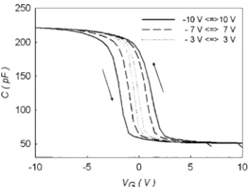
The SiGeN layer of a MOIOS memory device is utilized to capture the injected carriers from the channel, which causes a variation in the threshold voltage of the memory device. Figure 2 shows the capacitance-voltage共C-V兲 hyster-esis of the MOIOS structure. The electrical C-V measure-ments are performed by bidirectional voltage sweeping. The sweeping conditions were split as follows,共i兲 operated from 10 to −10 V, and reversely, 共ii兲 from 7 to −7 V and re-versely, as well as 共iii兲 from 3 to −3 V and reversely. It is clearly shown in Fig. 2 that the threshold-voltage shift 共memory window, ⌬Vt兲 of the MOIOS structure is
promi-nentfor 900 䊐 oxidation. When the device is programmed, the electrons directly tunnel from the Si substrate through the tunnel oxide, and are trapped in the forbidden gap of the SiGeN layer. For the erasion operation, the holes may tunnel from the valence band of the Si substrate and recombine with the electrons trapped in the SiGeN layer. The blocking oxide is utilized to prevent the carriers of gate electrode from in-jecting into the charge-trapping layer by Fowler-Nordheim 共FN兲 tunneling. The threshold-voltage shift after the 7 V pro-gramming operation is 2 V for the SiGeN memory device with a-Si layer layer oxidized at 900䊐. The large threshold voltage shift of memory device with oxidized a-Si film as blocking oxide layer is attributed to the presence of rich charge-trapped sites in the SiGeN film. When electrons are captured in the charge-trapping sites of the SiGeN film, a large threshold voltage shift is shown for a memory device. FTIR spectra of the SiGeN stack film following the oxidation of amorphous silicon layer are schematically shown in Fig. 3. It is found the Si-H, Ge-H, N-H, Si-N, and Ge-N bonds are present in the SiGeN film, respectively. The trap-rich material can supported more trap site for charge storage. Hence, the memory windows were formed after programmed for the proposed material SiGeN in this experiment.
For the SiO2 originated from oxidized a-Si film, there
are dangling bonds or defects exist in the bulk and at the interface between SiGeN and SiO2 layer. The electrons
trapped near the channel will dominate the threshold voltage significantly than those far from the channel. The proposed
SiGeN stack layer with high-temperature oxidized a-Si layer, therefore, contributes both larger memory window and the additional blocking oxide deposition for the nonvolatile memory application promisingly. The reliability issue of the MOIOS memory device is currently under investigation to promote the SiGeN-based nonvolatile memory as a candidate of the distributed charge storage memory device.
In conclusion, the ease technology to form SiGeN stack film with both distributed storage elements and upside block-ing oxide has been demonstrated successfully for memory application. The memory windows after programming were resulted from the retainable dangling bonds, such as Si-H and Ge-H bonds. There is 2 V threshold voltage shift under 7 V write operation, which is sufficient for a memory device to define the signal “0” and “1” The new material of SiGeN severed as charge trapping layer was proposed and per-formed in this study.
This work was performed at National Nano Device Laboratory and was supported by the National Science Council of the Republic of China under Contract Nos. NSC94-2215-E009-063, NSC94-2215-E009-031, and NSC94-2120-M-110-005. Also, the authors would like to ac-knowledge the support of the Plasma Enhanced Chemical Vapor Deposition共PECVD兲 system in National Chiao Tung University共NCTU兲 in HsinChu. Furthermore, this work was partially supported by ChungHwa Picture Tubes, Ltd.共CPT兲 and MOEA Technology Development for Academia Project No. 94-EC-17-A-07-S1-046.
1D. Kahng and S. M. Sze, Bell Syst. Tech. J. 46, 1288共1967兲. 2J. D. Blauwe, IEEE Trans. Nanotechnol. 1, 72共2002兲.
3S. Tiwari, F. Rana, K. Chan, H. Hanafi, C. Wei, and D. Buchanan, Tech. Dig. - Int. Electron Devices Meet. 1995, 521.
4Y. C. King, T. J. King, and C. Hu, Tech. Dig. - Int. Electron Devices Meet.
1998, 115.
5J. J. Welser, S. Tiwari, S. Rishton, K. Y. Lee, and Y. Lee, IEEE Electron Device Lett. 18, 278共1997兲.
6M. H. White, D. A. Adams, and J. Bu, IEEE Circuits Devices Mag. 16, 22 共2000兲.
7M. H. White, Y. Yang, A. Purwar, and M. L. French, IEEE Int’l Nonvola-tile Memory Technology Conference, 52共1996兲.
8V. A. Gritsenko, S. N. Svitasheva, I. P. Petrenko, Hei Wong, J. B. Xu, and I. H. Wilson, J. Electrochem. Soc. 146, 780共1999兲.
9Y. C. King, T. J. King, and C. Hu, IEEE Electron Device Lett. 20, 409 共1999兲.
10L. Dori, A. Acovic, D. J. Dimaria, and C. H. Hsu, IEEE Electron Device Lett. 14, 283共1993兲.
11M. Rosmeulen, E. Sleeckx, and K. D. Meyer, Tech. Dig. - Int. Electron Devices Meet. 2002, 189.
12S. Wolf, Silicon Processing For The VLSI Era, 2nd ed.共Lattice Press, Sunset Beach, California, 1999兲, Vol. 1, p. 706.
FIG. 2. The capacitance-voltage共C-V兲 hysteresis of the MOIOS structure. The electrical C-V measurements are performed by bidirectional voltage sweeping共1兲 from 10–共−10兲 V and 共−10兲–10 V; 共2兲 from 7–共−7兲 V and 共−7兲–共7兲 V; 共3兲 from 3–共−3兲 V and 共−3兲–3 V.
FIG. 3. FTIR spectra of the SiGeN stack before a-Si layer deposition.
112105-2 Tu et al. Appl. Phys. Lett. 88, 112105共2006兲
This article is copyrighted as indicated in the article. Reuse of AIP content is subject to the terms at: http://scitation.aip.org/termsconditions. Downloaded to IP: 140.113.38.11 On: Thu, 01 May 2014 02:05:51