This content has been downloaded from IOPscience. Please scroll down to see the full text.
Download details:
IP Address: 140.113.38.11
This content was downloaded on 25/04/2014 at 01:06
Please note that terms and conditions apply.
View the table of contents for this issue, or go to the journal homepage for more 2011 J. Phys.: Conf. Ser. 301 012053
On-
chip detection circuit for protection design in display
panel against electrical fast transient (EFT) disturbance
Cheng-Cheng Yen1, Ming-Dou Ker 1, 2, Wan-Yen Lin1, Che-Ming Yang3,
Shih-Fan Chen3, and Tung-Yang Chen3
1 Institute of Electronics, National Chiao-Tung University, 1001 Ta-Hsueh Road,
Hsinchu, 30010, Taiwan
2 Department of Electronic Engineering, I-Shou University, No.1, Sec. 1, Syuecheng
Road, Dashu Township, Kaohsiung, 84041, Taiwan
3 Research and Development Center, Himax Technologies, Inc., 26 Zih-Lian Road,
Tree Valley Park, Tainan, 74445, Taiwan E-mail: [email protected]
Abstract. A new on-chip detection circuit is proposed for electrical fast transient (EFT)
protection design in a display system. For microelectronic products, electrical transient disturbances often cause upset or frozen states under the IEC test standard. The output signal of the proposed detection circuit can be used as a firmware index to execute system automatic recovery operations and to release the EFT-induced locked states in display panels. The circuit function to detect positive or negative electrical transients has been investigated in HSPICE simulation and verified in silicon chip. The experimental results have confirmed successful circuit performance under EFT tests. With hardware/firmware co-design, the immunity of a display system against electrical transient disturbance has been significantly improved.
1. Introduction
Electrical fast transient (EFT) event has become an important reliability issue to display systems equipped with CMOS driver integrated circuits (ICs) [1], [2]. This tendency results from not only the progress of more functions integrated into a single silicon chip but also from the strict requirements of reliability test standards, such as the EFT test. The microelectronic product must sustain the EFT voltage level of ±2 kV under EFT tests to achieve the immunity requirement of “level 4” in the IEC 61000-4-4 test standard [3]. When some real-world EFT events occurred, the power lines of the CMOS ICs in the microelectronic products no longer maintained normal voltage levels, but an exponential voltage pulse with the amplitude of several tens volts occurred. The waveform of a single EFT pulse has a rise time of about 5 ns and the pulse duration of 50 ns. The CMOS ICs inside the microelectronic products are very susceptible to electrical transient disturbance [4]-[8], even though they have passed the component-level ESD specifications.
In this work, an on-chip detection circuit is designed to detect electrical transient disturbance under EFT tests and verified in a 0.13-m CMOS process. The proposed circuit can provide a hardware/firmware co-design solution to improve the susceptibility of microelectronic display systems against EFT-induced electrical transient disturbance.
2. On-Chip Detection Circuit
2.1. Circuit Implementation
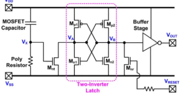
In this work, an on-chip detection circuit has been proposed, as shown in Fig. 1. The CR-based circuit structure is designed to detect EFT-induced transient disturbance. The NMOS (Mnr) is used to set the
initial output voltage levels at nodes VOUT and VA as 1.8 V with the VDD of 1.8 V. During the normal
operating condition, the node VX is biased at 0 V by connecting to the VSS line through a poly resistor.
The two-inverter latch is designed to memorize the logic state before and after EFT events. The MOSFET capacitor is a PMOS device and connected between the VDD line and the node VX to sense
transient disturbance coupled to the 1.8-V power line. For the buffer stage, there are three inverters designed in series to drive the 8-pF loading capacitance of the voltage probe at node VOUT. Under the
EFT tests with an overshooting transient voltage, the node VX will be coupled with positive voltage by
the MOSFET capacitor coupling. Then, the NMOS device (Mnt) will be turned on by the overshooting
EFT voltage to pull down the voltage level at the node VA from 1.8 V to 0 V. Therefore, the logic level
stored at the node VB can be further pulled up from logic “0” to logic “1” to memorize the EFT events.
With the buffer inverters, the final output voltage of the proposed detection circuit is changed from logic “1” to logic “0” to detect the occurrence of EFT-induced transient disturbance.
The simulation conditions and measurement setup for the EFT test combined with the attenuation network is shown in Fig. 2. The EFT generator is connected to the VDD line of the device under test
(DUT) through -40dB attenuation network. The VDD and VOUT transient responses of the detection
circuit are monitored by the digital oscilloscope.
Figure 1. The proposed on-chip detection circuit.
Figure 2. Measurement setup and simulation conditions for EFT test combined with -40dB attenuation network.
2.2. HSPICE Simulation
For HSPICE simulations, with the proper parameters (including the rise time constant τ1 (=3 ns), fall
time constant τ2 (=25 ns), rise time delay td1 (=200 ns), fall time delay td2 (=210 ns), initial dc voltage
value V1 (=1.8 V), and exponential pulse voltage value V2), the exponential voltage pulse can be
constructed to simulate the EFT-induced disturbance under EFT tests. The rising edge of this exponential time-dependent voltage pulse is expressed as
2
1 ( ) 1 1 1 2 1 ( ) 1 exp , when . d p rise d d V t V V V t t t t t (1)The falling edge of this exponential time-dependent voltage pulse is expressed as
2
1
1 2
( ) 1 1 2 2
1 2
( ) 1 exp 1 exp , when t .
d d p fall d V t V V V t t V V t t t (2) 2
The simulated VDD and VOUT waveforms of the proposed on-chip detection circuit with positive and
negative exponential pulse transient disturbance on VDD line are shown in Figs. 3(a) and 3(b),
respectively. From the simulated waveforms, VDD begins to change rapidly from 1.8 V and acts with
positive or negative exponential voltage pulse waveform during the simulated transient disturbance on power line. During EFT zapping conditions, VOUT is disturbed simultaneously during the EFT-induced
disturbance in the simulation. After VDD finally returns to its normal voltage level of 1.8 V, VOUT will
be changed from 1.8 V to 0 V, as shown in Figs. 3(a) and 3(b). In future works, the variation of transistor parameters should be taken into design considerations.
(a) (b) Figure 3. Simulated VDD and VOUT waveforms of the proposed on-chip detection circuit under EFT
tests with (a) positive, and (b) negative, exponential voltage pulse waveforms coupled to VDD.
3. Experimental Results
The measured VDD and VOUT waveforms of the on-chip detection circuit under EFT test with EFT
voltage of +200 V and -350 V are shown in Fig. 4(a) and 4(b), respectively.. As shown in Fig. 4(a) (Fig. 4(b)), under the EFT test with positive (negative) EFT voltage, VDD begins to increase (decrease)
rapidly from 1.8 V. Meanwhile, VOUT begins to greatly increase (decrease) with positive (negative)
exponential voltage pulse coupled on VDD line. Finally, after the EFT-induced transient disturbance,
the final output voltage (VOUT) of the detection circuit is changed the logic “1” to logic “0.”
(a) (b) Figure 4. Measured VDD and VOUT waveforms on the proposed on-chip detection circuit under EFT
4. Application in Display Systems
The high-voltage electrical fast transients often cause CMOS ICs inside the equipment under test (EUT) to be upset or frozen after the system-level electrical transient disturbance. It has been reported that electrical transient disturbance coupled to power and ground pins of a super twisted nematic (STN) liquid crystal display (LCD) driver circuit can cause abnormal function of the LCD panel. The transient disturbance energy can couple through the indium tin oxide (ITO) film from the LCD panel into the CMOS driver ICs to cause display malfunction.
In this work, the proposed on-chip detection circuit can cooperate with firmware operation to provide hardware/firmware co-design for improving the robustness of the display products against EFT-induced stresses. The detection results can be used as firmware index to execute an automatic recovery procedure when display products are disturbed with EFT events. The detection circuit can connect with the 1.8-V power line to detect and memorize the occurrence of EFT-induced transient disturbances coupled on the digital subsystem of display products. In the beginning, the output (VOUT)
state of the detection circuit is set to logic “1” by the power-on procedure. When the electrical transients happen, the output state (VOUT) of the detection circuit will transit from 1.8 V to 0 V.
Simultaneously, firmware recovery procedure can be started to restore the display system to a known stable state as soon as possible. After the recovery procedure, the output level of the detection circuit and the firmware index are both re-set to logic “1” again for detecting the next EFT-induced electrical transient disturbance event.
5. Conclusions
An on-chip detection circuit to memorize EFT events has been proposed and successfully verified in a CMOS 0.13-µm process. The circuit performance under different positive and negative EFT-induced transient disturbance has been investigated by HSPICE simulation. The experimental results in silicon chip have confirmed that the proposed detection circuit can successfully detect and memorize the occurrence of fast electrical transients during EFT tests. The proposed detection circuit can be further combined with firmware design to provide an effective solution against the frozen or locked states caused by EFT-induced transient disturbance events in microelectronic display products.
Acknowledgments
This work was partially supported by National Science Council, Taiwan, under Contract NSC 99-2811-E-009-051; and by Himax Technologies Inc., Taiwan.
References
[1] A. Wallash and V. Kraz, “Measurement, simulation and reduction of EOS damage by electrical fast transients on AC power,” in Proc. EOS/ESD Symp., 2010, pp. 59–64.
[2] M.-D. Ker and S.-F. Hsu, Transient-Induced Latchup in CMOS Integrated Circuits, John Wiley & Sons, 2009.
[3] IEC 61000-4-4 Standard, “EMC – Part 4-4: Testing and Measurement Techniques –
Electrostatic Fast Transient/Burst Immunity Test,” IEC, 2004.
[4] W. Huang, J. Dunnihoo, and D. Pommerenke, “Effects of TVS integration on system level ESD robustness,” in Proc. EOS/ESD Symp., 2010, pp. 145–149.
[5] K. Muhonen, P. Erie, N. Peachey, and A. Testin, “Human metal model (HMM) testing, challenges to using ESD guns,” in Proc. EOS/ESD Symp., 2009, pp. 387–395.
[6] E. Grund, K. Muhonen, P. Erie, and N. Peachey, “Delivering IEC 61000-4-2 current pulses through transmission lines at 100 and 330 ohm system impedances,” in Proc. EOS/ESD Symp., 2008, pp. 132–141.
[7] M. Honda, “Measurement of ESD-gun radiated fields,” in Proc. EOS/ESD Symp., 2007, pp. 323–327.
[8] T. Smedes, J. Zwol, G. Raad, T. Brodbeck, and H. Wolf, “Relations between system level ESD and (vf-) TLP,” in Proc. EOS/ESD Symp., 2006, pp. 136–143.