多媒體串列處理器之分散式記憶體管理單元設計
62
0
0
全文
(2) 多媒體串列處理器之分散式記憶體管理單元設計 Distributed Memory Management Unit Design for Media Stream Processor Architecture. 研 究 生:鄭漳源 指導教授:闕河鳴. Student:Chang-Yuan Cheng Advisor:Dr. Herming Chiueh. 博士. 國 立 交 通 大 學 電 信 工 程 學 系 碩 士 班 碩 士 論 文. A Thesis Submitted to Department of Communication Engineering College of Electrical Engineering and Computer Science National Chiao Tung University in Partial Fulfillment of the Requirements for the Degree of Master of Science in Communication Engineering October 2005 Hsinchu, Taiwan. 中華民國九十四年十月.
(3) 多媒體串列處理器之分散式記憶體管理單元設計 研究生:鄭漳源. 指導教授:闕河鳴 博士. 國立交通大學 電信工程學系碩士班. 摘要. 在現今多媒體應用上,影像處理、視訊壓縮、二維和三維繪圖、資料 複製和資料搬移是常見的程序。然而,處理器和記憶體之間的頻寬差距造成 傳輸資料減速。為了縮短現今多媒體影像處理架構上的差距,這篇論文提出 了一個分散式記憶體管理單元。分散式記憶體管理單元包含位址轉換單元和 雙倍資料率記憶體控制器。位址轉換單元提供一個虛擬記憶體機制和用來節 省資料傳輸時間。雙倍資料率記憶體控制器用於簡易地爆發讀取和寫入模 式。從分散式記憶體管理單元實現的結果顯示,當傳送十六百萬位元組資料 量時,提出的位址轉換單元架構比傳統的位址轉換單元速度提升了二百萬 倍。然而,當資料量小於十六百萬位元組時,無位址轉換單元傳輸時間與有 位址轉換單元傳輸時間相比會隨著資料量的增加而增加。本篇論文便是針對 現今多媒體應用架構中,用微量增加的電路面積和功率消耗以換取資料傳輸 效能的躍進。. I.
(4) Distributed Memory Management Unit Design for Media Stream Processor Architecture Student: Chang-Yuan Cheng. Advisor: Dr. Herming Chiueh. Department of Communication Engineering National Chiao Tung University Hsinchu, Taiwan. Abstract In modern multimedia applications such as image processing, video compression, two-dimension and three-dimension graphics, data copying and data moving are common processes. However, the bandwidth gaps between processors and memory cause the slow down of transition data. In order to bridge the gap, this thesis proposed a distributed memory management unit (DMMU) for modern media processing architectures. The DMMU consists of address translation unit (ATU) and double data rate (DDR) memory controller. The ATU provides a virtual memory mechanism, and been used to save data transition time. The DDR memory controller is used in simply burst read and burst write mode. The result of DMMU implementation shows that proposed ATU architecture provides 2 million times speed-up than conventional ATU when transmitted 16MB data size. However, when the data capacity is less than 16MB, the proportion of the transition time without ATU/ ATU is increased for the data capacity. The proposed design provides a leap up in data transition for modern media processing architecture with a tiny overhead in circuit area and power. II.
(5) Acknowledgments 本篇論文能夠順利完成,首先最要感謝的是我的指導教授闕河嗚博士。闕老 師在我研究上遇到問題時總能適時的提供意見,使我能得以突破窘境。另外,老 師注重的是學生能夠獨立思考問題與面對問題時該有的處理態度與應變能力,使 得我在研究領域上獲益良多。 其次,感謝偉閔、庭瑋、明崇、芳如四位同學在我的研究與生活上,給予的 幫助與鼓勵,使我能夠獲得更多的知識與技術。在此也謝謝祐誠、景鴻學長在工 作站管理與研究領域的指導,幫助我能夠順利的解決問題,也感謝明治、志軒、 書豪、智閔學長與實驗室學弟對我的幫助,讓我有一個難忘的研究生涯。 最後,我要感謝父母的支持與栽培與兄姊的鼓勵,和其他關心我的朋友,唯 有藉著大家的鼓勵,才能造就今日的我。 我誠心感謝上述提攜或幫助過我的你們,謝謝大家並祝福大家。. 鄭漳源 中華民國九十四年十月於新竹. III.
(6) Contents 中文摘要 English Abstract Acknowledgments Contents List of Tables List of Figures. Ⅰ Ⅱ Ⅲ Ⅳ V Ⅵ. _________. Chapter1 Introduction 1.1 Motivation 1.2 Organization. 1 1 4. Chapter2 DMMU Design Architecture. 5. 2.1 Data Copying and Data Moving in Address Translation Unit 2.2 Distributed Memory Management Unit 2.3 Address Translation Unit 2.4 DDR Memory Controller 2.4.1 Device Operations of DDR SDRAM 2.4.2 Mode Register Definition of DDR SDRAM 2.4.3 Block Diagram of DDR Memory Controller 2.4.4 The Main Controller Module 2.4.5 Summary. 5 7 9 12 12 15 16 17 19. Chapter3 Implementation. 20. 3.1 Computer-Aided Design Flow 3.2 Implementation of DMMU Interface 3.3 Circuit Verification 3.4 Functional Verification 3.5 Performance Evaluation 3.5.1 Comparison 3.6 Summary. Chapter4 Conclusions Bibliography. 20 23 25 29 45 45 49. ____. IV. 51 52.
(7) List of Tables Table 2.1 The supervisor and users access privileges and correspond to PR bits Table 3.1 The signals on the DMMU interface Table 3.2 The results of the ATU synthesis Table 3.3 The results of the DMMU synthesis Table 3.4 The results of the P&R in core utilization = 0.7 Table 3.5 The results of the P&R in core utilization = 0.8 Table 3.6 The core area of the P&R results between the different core utilization and clock frequency Table 3.7 The specification table of the design Table 3.8 The different parameter values during initial states Table 3.9 The different parameter values during command states Table 3.10 The test bench of the ATU Table 3.11 The clock period of the micro-controller, the DMMU and DDR Table 3.12 The data transition time of data copying and data moving in the different data capacity without ATU Table 3.13 Total access time of two ATU modes. V. 12 24 26 26 27 27 27 28 30 30 33 46 46 48.
(8) List of Figures Figure 1.1 The performance gap of CPU and memory Figure 1.2 Bandwidth hierarchy of an imagine stream architecture Figure 1.3 Time to complete a series of memory references without access scheduling Figure 1.4 Time to complete a series of memory references with access scheduling Figure 1.5 Memory access scheduler architecture Figure 2.1 The page table of traditional address translation Figure 2.2 The proposed ATU mechanism in the DMMU Figure 2.3 The proposed DMMU micro-architecture in the streaming memory system of the imagine stream processor Figure 2.4 The proposed memory system Figure 2.5 The block diagrams of the DMMU micro-architecture Figure 2.6 The flows of the address translation Figure 2.7 The stream register file organization Figure 2.8 The translation table of the address translation mode Figure 2.9 The block diagram of DDR SDRAM 512Mb B-die Figure 2.10 The simplified state diagram of the DDR SDRAM Figure 2.11 The mode register set of DDR SDRAM Figure 2.12 The functional block diagram of the DDR memory controller Figure 2.13 Initial state diagram of DDR memory controller Figure 2.12 The command state diagram of DDR memory controller Figure 3.1 The cell-base design flow Figure 3.2 The physical level design flow Figure 3.3 The DMMU interface Figure 3.4 Layout of DMMU Figure 3.5 The operation environment of DMMU functional verification Figure 3.6 The initial state machine of DDR memory controller Figure 3.7 The burst write and burst read mode of DDR memory controller Figure 3.8 Access data (PR = 2’b00) under supervisor mode in the DMMU Figure 3.9 Access data (PR = 2’b01) under supervisor mode in the DMMU Figure 3.10 Access data (PR = 2’b10) under supervisor mode in the DMMU Figure 3.11 Access data (PR = 2’b11) under supervisor mode in the DMMU Figure 3.12 Access data (PR = 2’b00) under users mode in the DMMU Figure 3.13 Access data (PR = 2’b01) under users mode in the DMMU VI. 1 2 3 3 3 6 6 8 8 9 9 10 11 13 15 16 17 18 19 21 22 23 28 29 31 32 35 36 37 38 40 41.
(9) Figure 3.14 Access data (PR = 2’b10) under users mode in the DMMU Figure 3.15 Access data (PR = 2’b11) under users mode in the DMMU Figure 3.16 Data capacity over limitation in the DMMU Figure 3.17 Test configuration environment Figure 3.18 The access time versus the data capacity for different ATU Figure 3.19 The proportion of the access time without ATU/ATU versus the different data capacity. VII. 42 43 44 45 48 49.
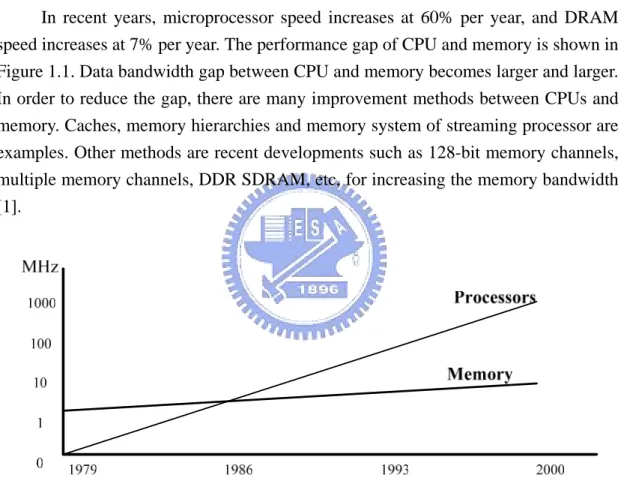
(10) .. Chapter 1 Introduction 1.1 Motivation In recent years, microprocessor speed increases at 60% per year, and DRAM speed increases at 7% per year. The performance gap of CPU and memory is shown in Figure 1.1. Data bandwidth gap between CPU and memory becomes larger and larger. In order to reduce the gap, there are many improvement methods between CPUs and memory. Caches, memory hierarchies and memory system of streaming processor are examples. Other methods are recent developments such as 128-bit memory channels, multiple memory channels, DDR SDRAM, etc, for increasing the memory bandwidth [1].. Figure 1.1 The performance gap of CPU and memory. Multimedia applications are popular nowadays. They are characterized by large available parallelism, little data reuse, and high computation to memory access [2][9]. In high computation to memory, data are continuously loaded to CPUs and stored to memory. Therefore, performance gap between CPU and memory will worsen data bandwidth more severely in multimedia applications. In related researches of multimedia applications, many kinds of architecture are used to solve the problem [3][4]. For instance, the imagine stream processor is proposed by Stanford University [5]. 1.
(11) As shown in Figure 1.2, the imagine stream processor is characterized by data bandwidth hierarchy. It scales the provided bandwidth across the levels of the storage hierarchy. The different bandwidths are expressed among the local register files (LRF), stream register file (SRF) and SDRAM, respectively. They are used to solve the performance gap between ALU cluster and memory. When access instructions are issued in stream processor, data must be loaded to SRF or stored to SDRAM [6]. Therefore, data copying and data moving are needed to frequently load and store data in imagine stream processor.. Streaming memory. SDRAM SDRAM SDRAM SDRAM. 2GB/s. Stream Register File. LRF ALU Cluster ALU Cluster. ALU Cluster ALU Cluster. 32GB/s. 544GB/s. Figure 1.2 Bandwidth hierarchy of an imagine stream architecture [6]. In order to save the access time of data loading and storing, the memory access scheduling architecture is proposed in the memory system of the stream processor [7]. It is used to schedule memory references to optimize memory system. Suppose the sequence is composed of eight memory references as shown in Figure 1.3. Each memory reference consists of bank, row and column. Every access is needed 3 cycles to precharge a bank, 3 cycles to access a row of a bank, and 1 cycle to access a column of a row. If these eight memory references are performed in order, they will take 56 cycles to complete the total eight references. If eight memory references are scheduled as shown in Figure 1.4, they will totally take 19 cycles [7]. As shown in Figure 1.5, memory access scheduling is the process of ordering the DRAM operations (bank precharge, row activation, and column access) necessary to complete the set of currently pending memory references. Through reordering DRAM operations, the memory system can save access time on waiting previous process [7].. 2.
(12) Figure 1.3 Time to complete a series of memory references without access scheduling [7].. Time (Cycles) 1 2 3 4 5 6 7 8 910111213141516171819 (0.0.0) P A C (0.1.0) P A C (0.0.1) (0.1.3) (1.0.0) (1.1.1) (1.0.1) (1.1.2). C C. P. A. C. P. A. C. C C. Figure 1.4 Time to complete a series of memory references with access scheduling [7]. V L/S Row Col Data State Precharge0 Bank 0 Pending References. Row Arbiter0 Column Arbiter. Memory References. Memory Access Scheduler Logic. Address Arbiter. DRAM Operations. V L/S Row Col Data State Bank N Pending References. Row ArbiterN PrechargeN. Figure 1.5 Memory access scheduler architecture [7]. Furthermore, when many users simultaneously access data that are included of video, audio, still images and other data-intensive data, data copying and data moving are more common operations. Therefore, they will waste much time to load and store 3.
(13) even if they use memory access scheduling. On the other hand, fast data copying and data moving are needed on streaming processor. In order to improve the performance of data transition in the imagine stream processor, a distributed memory management unit (DMMU) is proposed in this thesis. DMMU includes with address translation unit (ATU) and the DDR memory controller. In traditional address translation, the translated table only defines the mapping physical address, such as page table [1][13]. The page corresponds to physical address is fixed, so that data copying and data moving are needed to transit to required address. Therefore, if the instruction of data transition is issued, data is transited from original physical address to goal physical address. However, this proposed ATU contains a novel segment table mechanism, which users can flexibly define, for fast data copying and data moving. As the instruction of data transition is issued, the goal physical address is invariant. The segment needs to be mapped from the original segment to target segment. Therefore, the same data is found through the segment access. The advantage of the proposed ATU saves the data transition time through segment mapping. In this thesis, one of our goals is to design an efficient ATU. The flexible segment table which consists of variable segment size, protection privilege, boundary check, and validity reforms the data transition mechanism. Take advantage of the proposed ATU to achieve the fast data copying and data moving. The other of our goals is to integrate ATU and DDR memory controller in stream processor.. 1.2 Organization This thesis is organized as following: In Chapter 2, the detail design of the distributed memory management unit is presented. In Chapter 3, the implementation of the DMMU is described in detail. The functional verification and performance evaluation are presented. In Chapter 4, the conclusions of DMMU and the future work are presented.. 4.
(14) Chapter 2 DMMU Design Architecture The architecture of the distributed memory management unit (DMMU) design is presented in this chapter. It is composed with an address translation unit (ATU) and a DDR memory controller. In Section 2.1, the improved of data copying and data moving mechanisms between the proposed address translation and a traditional address translation are presented. In Section 2.2, the DMMU micro-architecture is presented to improve the memory system of the streaming processors. The DMMU increases the speed of the data transition in streaming processors. The ATU of the DMMU translates from virtual address to physical address [10]. The basic building blocks of ATU will be explained in Section 2.3. The DDR memory controller is used with simply burst read or burst write command [11]. In Section 2.4, the functional units of the DDR memory controller are expressed for how to operate in read or write command.. 2.1 Data Copying and Data Moving in Address Translation Unit In traditional address translation, the virtual address is translated to physical address corresponds to a translated table, such as page table [1][13]. As shown in Figure 2.1, the virtual address is broken into virtual page number and page offset [1][13]. At first, the virtual page number corresponds to the entry of the page table. As the entry is selected, the physical page number of page table is mapped to physical memory or disk storage. When instruction of load and store are issued, data could be found at corresponding memory or disk storage. However, when instruction of data transition is issued, data is transited from original physical address to target physical address. Because the translated table of the traditional address translation is fixed, data copying and data moving are needed to transit to required address. The access time of traditional address translation is wasted for data transition. Therefore, in order to save the data transition time, a new address translation is proposed. Data copying and data moving are not needed to transit, they only need segment mapping. 5.
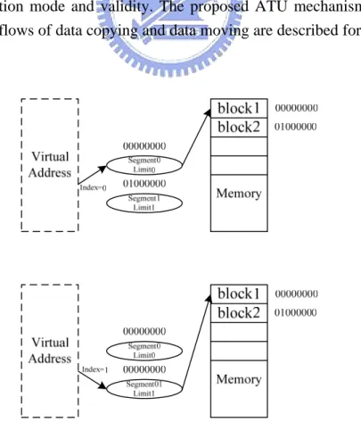
(15) Virtual page number. Page table Valid. Physical memory. Physical page number. 1 1 1 1 0 1 1 0 0. Disk storage. Figure 2.1 The page table of traditional address translation [1][13]. The data transition of the proposed ATU is described in below. The mechanism transfers from the virtual address to the physical address. The segment base defines the start location of the DDR SDRAM and the limit base defines the maximum data capacity, protection mode and validity. The proposed ATU mechanism is shown in Figure 2.2. The flows of data copying and data moving are described for the operation process.. Figure 2.2 The proposed ATU mechanism in the DMMU. 6.
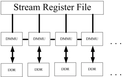
(16) For an example, if the instruction of data copying is issued, the micro-controller loads the segment0 and the limit0 in register files first. Next, the segment0 and limit0 of the register files store into the segment1 and the limit1. After the segment1 and the limit1 are completed setup, the address would be issued by the micro-controller. When the micro-controller issues the new address to ATU, the index of the virtual address will be pointed to the segment1 and the limit1. Then, the virtual address is transferred to the same physical address of DDR SDRAM. It saves the transition time for copying data from the block1 to the block2, but it wastes time to access the segment and limit register files. Finally, the ATU checks the protection bits of the segment0 and segment1. If the protection modes of the two segments are operated on “read only”, they will work normally in streaming processing. Else the error will be generated with an exception in the streaming processing. The mechanism of data moving is similar to data copying. The only one different with data copying on the proposed ATU is the original segment0 and limit0 will be updated by the users. The valid bit would be set “low” to refuse the original access. In the above operations of the traditional and the proposed address translation, determine the access time of data copying and data moving depending on the data transition. The proposed DMMU is used to increase data transition efficiency in multimedia applications.. 2.2 Distributed Memory Management Unit The proposed DMMU micro-architecture, which improves data transition time in the streaming memory system of the media stream architecture, is shown in Figure 2.3. The improved streaming architecture consists of micro-controller, ALU Cluster, Stream Register Files (SRF), network interface, address translation unit, DDR memory controller, parcel network and off-chip DDR SDRAM. When stream data is transmitted between SRF and off-chip DDR SDRAM, the required data is needed to load and store to SRF. Furthermore, when the stream data is transited between off-chip DDR SDRAM and off-chip DDR SDRAM, the required data is not needed to load and store to SRF. The characteristics of the DMMU are variable-sized segment register files, fast data copying and fast data moving. On the ATU mechanism, the users can flexibly define the segment sizes for the different data lengths of the media streaming data. So, the DMMU is the irregular memory access mechanism which can suit the variable-sizes streaming data. 7.
(17) Figure 2.3 The proposed DMMU micro-architecture in the streaming memory system of the imagine stream processor. The proposed memory system which consists of the DMMU and a parcel network mechanism is shown in Figure 2.4. The DMMU supports in-memory address translation. When data is copied and moved in the same off-chip memory, the micro-controller can control the DMMU to save much time to load or store data. When data is accessed in the different off-chip memory, it would be needed a parcel network to communicate each other. Parcels are transmitted through a separate DMMU-to-DMMU interconnection to enable communication without interfering with host-memory traffic [12][13]. To avoid saturation of the memory bus, DMMU-to-DMMU communications occur primarily by means of a distinct high bandwidth network between the DMMU and DMMU. Through the network mechanism, it could be easily accomplished on data transition.. Figure 2.4 The proposed memory system. 8.
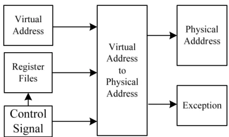
(18) The block diagrams of the DMMU micro-architecture are shown in Figure 2.5. The DMMU consists of the virtual address, register files, control signal, virtual address to physical address mechanism, physical address and exception in the ATU and the clock generator, control signal and data signal in DDR memory controller module.. Figure 2.5 The block diagrams of the DMMU micro-architecture.. 2.3 Address Translation Unit The ATU is an address translation mechanism that translated virtual addresses to physical addresses [10]. The flows of the address translation are shown in Figure 2.6.. Figure 2.6 The flows of the address translation. 9.
(19) Before the address translation, the boundary of the data length limitation is needed to decide in our design. The stream register file organization is diagramed in Figure 2.7 [5]. The SRF contains a 128 KB SRAM organized as 1024 blocks of 32 words of 32 bits each. So the minimum boundary of the data length limitation must be more than 128 KB. Since the minimum boundary of the data length limitation is 32’h00007FFF. The maximum boundary of the data length limitation is dependant on the data capacity of the DDR SDRAM. For an instance, when the data capacity of DDR SDRAM is 256 MB, the maximum boundary of the data length limitation is 32’h03FFFFFF. However, the maximum limitation is not the entire block size of the DDR SDRAM. It can be flexible defined according to users. For an instance, it could be 256 MB, 64 MB or 512KB …etc. It only normally translates from virtual address to physical address between the maximum and minimum boundaries.. Figure 2.7 The stream register file organization [5]. From Figure 2.6, the basic function units of the ATU consist of the virtual address, register files, control signal, virtual address to physical address mechanism, physical address and exception. The virtual address is composed with 32 bit. The register files are used to store the segment register files, limit register files, protection modes and validity. The segment register files decide the start location of the physical memory and the limit register files are checked of the virtual address offset which belongs to the limitation boundary. The protection modes are used to decide the privileges of the users and supervisor. The valid bit is represented the validity of the 10.
(20) segment. The control signal has four functions, which are the translation mode, user privilege, memory enable and read/write command. The translation modes are classified of address translation or without address translation. If the translation mode is the address translation mode, the virtual address will be translated to the physical address through segment mapped. The other translation mode, the without address translation mode is used to debugging or initialization, the virtual address is completely mapped to the physical address. The physical address is composed with 25 bits. The exception is checked of the boundary of the virtual address, segment validity and access privilege. The translation table of the address translation mode is shown in Figure 2.8. The index of the virtual address is used to select a segment of the table. The segment adds to the offset to form the physical address on Eq 2.1. The exception condition E for address translation is listed on Eq 2.2. If the offset of the virtual address exceeds the boundary of the limit registers, it will be sent an error to except this invalid virtual address. It could avoid mapping to null physical address.. Figure 2.8 The translation table of the address translation mode.. 11.
(21) PA = Segment Base + offset. (Eq 2.1). E = (va[0]∧ limit[3]) ∨ (va[1]∧ limit[4]) ∨ ⋅ ⋅ ⋅ ∨ (va[24]∧ limit[27]) ). (Eq 2.2). The supervisor and users access privileges and correspond to PR bits are expressed in table 2.1. When P bit is “high”, it is a supervisor privilege. On this level, the supervisor could read/write or read only with R bit is “low” or “high” and users could not access data on the situation. When P bit is “low”, users could read/write or read only with R bit is “low” or “high”. The supervisor could read/write in the privilege. Table 2.1 The supervisor and users access privileges and correspond to PR bits. Encoding of PR Bits. Supervisor Privilege. User Privilege. 00. RW(read-write). RW. 01. RW. RO(read only). 10. RW. None. 11. RO. None. 2.4 DDR Memory Controller This section described the elaboration of the DDR memory controller. The device operations of DDR SDRAM are reviewed. The initialization and command operations of DDR memory controller are showed in this Section. The command modes of our DDR memory controller support burst write and burst read modes.. 2.4.1 Device Operations of DDR SDRAM DDR SDRAM is the double data rate synchronous dynamic random access memory. From the speed increasing of the memory, DDR SDRAM transfers data on both the rising and falling edge of the clock [14][15][16]. The device operations and timing diagram of DDR SDRAM are referenced by SAMSUNG’s products [17]. The DDR SDRAM 512Mb B-die (x4, x8, x16) is showed for example. As shown in Figure 2.9, SDRAM is operated with complicated signals which consist of address, bank, chip select, row address strobe, column address strobe, write enable, clock, clock enable, data mask, data, and data strobe. By controlling those signals, the DDR SDRAM could be operated normally. Therefore, DDR memory controller would be used to simplify these numerous signals.. 12.
(22) LWE. CK , CK. CK , CK. RAS RAS. CK , CK. LWE. CS. CAS. CK , CK. RAS CAS WE. Figure 2.9 The block diagram of DDR SDRAM 512Mb B-die [17]. The simplified state diagram of the DDR SDRAM is shown in Figure 2.10 [17]. The device operations of DDR SDRAM are briefly described in below. They consist of state modes and access functionalities [17].. Power-up & Initialization Sequence: DDR SDRAM must be powered up and initialized before reading and writing command. When the initialization sequence is completed, the DDR SDRAM is ready to normal operation.. Mode Register Set (MRS): The mode register set stores control signals for operating modes of DDR SDRAM. It consists of CAS Latency , addressing mode, burst length, test mode, DLL reset. Users can define the information to control MRS modes.. Extended Mode Register Set (EMRS): The extended mode register set stores control signals for enabling or disabling DLL, and output driver impendence. The extended mode register set must be defined after power up for enabling or disabling DLL. 13.
(23) Precharge: The precharge command is used to precharge or close a bank. The precharge command can be used to precharge each bank respectively or all banks simultaneously.. No Operation (NOP) & Device Deselect: The operation of device deselect is used to ignore all inputs. NOP must wait 200us delay to finish the current operation before precharge command is issued.. Row Active: When banks are selected, the row activate would proceed with next step. Before write and read command are issued, row active must be ready.. Read Bank: This command is used after the row active command to initiate the burst read of data. The length of the burst and the CAS latency time will be determined depending on MRS mode.. Write Bank: This command is used after the row activate command to initiate the burst write of data. The length of the burst will be determined depending on MRS mode. The essential functionality is required for the DDR SDRAM device. They are included burst read operation, read interrupted by a precharge, write interrupted by a write, write interrupted by a read & dm, write interrupted by a precharge & dm, burst stop, dm masking, read with auto precharge, write with auto precharge, auto refresh & self refresh and power down. We will describe two operations that are burst read operation and burst write operation.. Burst Read Operation: Burst read operation in DDR SDRAM is continuously reading data. The address inputs (A0~A9) determine the starting address for the burst. The mode register sets type of burst (sequential or interleave) and burst length (2, 4, 8) are decided. The first output data is available after the CAS latency from the read command.. Burst Write Operation: Burst write operation in DDR SDRAM is continuously writing data. The mode register sets type of burst (sequential or interleave) and burst length (2, 4, 8) are decided. There is no write latency relative to DQS required for burst write cycle.. 14.
(24) Power Applied. Power On. Precharge PREALL. Self Refresh. REFS. RESX MRS MRS EMRS. REFA. Idle. Auto Refresh. CKEL Active Power Down. CKEH ACT CKEH. CKEL. Burst Stop. Row Active. Write. Write Write. Precharge Power Down. Read. Writ A Read A Read. Read Read. Writ A. Read A Read A PRE. Writ A. PRE. Read A. PRE. PRE. Pre Charge PREALL. Automatic Sequence Command Sequence. Figure 2.10 The simplified state diagram of the DDR SDRAM [17].. 2.4.2 Mode Register Definition of DDR SDAM In order to understand the DDR memory controller how to execute the read or write command, the mode register set of DDR SDRAM must be defined. The mode register which stores data for controlling the various operation modes of DDR SDRAM is shown in Figure 2.11. The mode register set is included burst length, addressing mode, burst type, CAS Latency, test mode, DLL reset [17]. The burst length uses A0~A2 to express three classifications of data length that are two, four or eight blocks of data. Addressing mode uses A3 to represent two classifications of burst types that are sequential and interleave. CAS Latency is the abbreviation of column address strobe latency that is meant read latency from column 15.
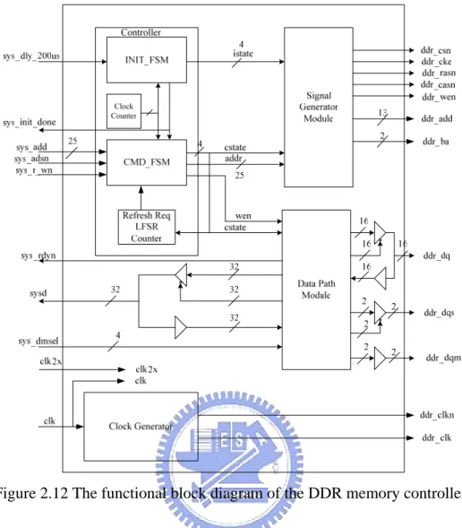
(25) address. The CAS Latency uses A4~A6 to represent 2, 2.5, or 3 clock cycles of CAS latency. A7 is expressed normal mode or test mode. DLL is the abbreviation of dynamic link library.A8 is used to control DLL reset. The parameters are eight blocks of data, sequential, and CAS Latency = 2, respectively. The parameter of data width is 32 bits on the user side and a half of data width is 16 bits on the DDR side.. CAS Latency. Figure 2.11 The mode register set of DDR SDRAM [17].. 2.4.3 Block Diagram of DDR Memory Controller The DDR memory controller which is combined with the ATU is used to simply read and write command in streaming processor. The functional block diagram of the DDR memory controller is shown in Figure 2.12. It consists of the main controller module, the signal generation module, the data path module and the clock generator module. The main controller module, which has a refresh counter, an initial and a command state machine are used to control the operation states of the DDR SDRAM. The signal generation module generates addresses, banks and control signals to DDR SDRAM. The data path module design interfaces between the DDR with a 16-bit data bus, and the bus master with a 32-bit data bus. The pattern generator generates two clock signals, one is clk (133MHz) and the other is clk2x (266MHz). The ddr_clk and ddr_clkn which are used to control active situations of DDR SDRAM are generated by clock generator. In next section, the parameters of mode register set in DDR SDRAM are defined.. 16.
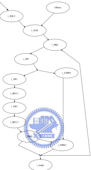
(26) Figure 2.12 The functional block diagram of the DDR memory controller.. 2.4.4 The Main Controller Module Before memory access could be executed, DDR SDRAM needs to initialize by a sequence of commands [17]. The INIT_FSM module deals with DDR SDRAM initialization. The initial state diagram of the DDR memory controller is shown in Figure 2.13. At first, the circuit must be reset. After reset, the stable situation of system will be checked. In order to steady power and clock, the delay is needed 200 us. After power and clock are stable, the NOP and precharge command are issued, respectively. The initialization starts with the precharge all banks. Through EMRS DLL enable, MRS DLL reset, Precharge all banks, first Auto Refresh, second Auto Refresh and MRS, the initial finite state machine goes to ready state and remains for the normal memory access. After initialization of state machine is completed, the write and read command are issued by command finite state machine [11].. 17.
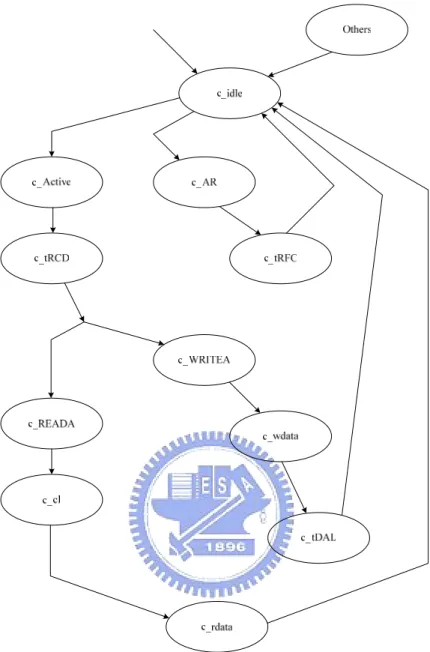
(27) Figure 2.13 Initial state diagram of DDR memory controller. The command state diagram of the DDR memory controller is shown in Figure 2.14. It deals with read, write and refresh of the DDR. During reset, the CMD_FSM state machine is initialized to idle. The Read/Write/Refresh cycle are operated in the command state machine, which performs read data from DDR SDRAM, write data to DDR SDRAM or auto refresh DDR SDRAM. The rows need to be selected before they could be accessed. However, only one row in the same bank could be selected at a time. Active command is used to select the rows and precharge (or the auto precharge hidden in the write and read commands as used in this design) is used to close the rows. When issuing the commands for opening or closing the rows, both row address and bank address need to be provided [11]. 18.
(28) Figure 2.14 The command state diagram of DDR memory controller.. 2.5 Summary The proposed DMMU micro-architecture, which improves data transition time in the streaming memory system of the media stream architecture, is introduced in this chapter. The operation processes of data copying and data moving is established. The ATU is described with data copying and data moving mechanism, variable segment size, protection privilege, boundary check, and validity. The DDR memory controller, which contains initial state and command state operation, supports simple burst write and burst read mode. The implementation of the DMMU which consists of circuit verification, function verification, and performance evaluation will be presented in next chapter. 19.
(29) Chapter 3 Implementation. The implementation of the DMMU architecture is expressed in this chapter. In Section 3.1, the CAD flow is introduced to understand the procedures of our design. The implementation of DMMU interface is demonstrated in Section 3.2. The verifications of the layout and the specification table are shown in Section 3.3. The functional verification and the performance evaluation are presented in Section 3.4 and 3.5, respectively. Finally, a summary is addressed in Section 3.6.. 3.1 Computer-Aided Design Flow The cell-base IC design flow is used to complete the design in the DDMU. The three levels of the design flow are shown in Figure 3.1 [1]. Our design is described with a behavioral level, a structural level and a physical level. The three levels are introduced in below. Behavioral level: When the block diagram of the architecture is designed, it must be considered the behavior mode. Not only functions are right in the design, but also the structural level and the physical level are estimated simultaneously. Structural level: The behavior mode of the design architecture is described by Verilog HDL (hardware description language). After the coding is correctly verified, the functional waveform of our design is simulated by Spring Soft Debussy. When the behavior simulation is completed, the logic synthesis is continued to transfer from Register-Transfer-Level (RTL) to gate-level netlists by Synopsys Design Compiler. We set the synthesis environments that are included operating environment, optimization constraints and optimization directives. We determine the critical constraints which area, power and timing must achieve the requirement of our design. Before the next level, the pre-layout simulation needs to check the netlists. If the waveform of the gate-level simulation is right, it represents that the structural level is completed. Else we would rebuild the RTL circuits and repeat the above steps. 20.
(30) Physical level: When we get the gate-level netlists, the next step of the design flow is generating the layout of DMMU. We use the Electronics Design Automation (EDA) tool to auto place and route (P&R) the circuit by Synopsys Astro. The physical level design flow is shown in Figure 3.2. These steps which include the design setup, the floorplanning, timing setup, post-placement optimization, clock tree synthesis, routing, design for manufacturing, design rule checking (DRC) & layout versus schematic (LVS), post-layout simulation and tape out. If there is any error in the verifications, the steps floorplanning, placement, or re-design the architecture need to be iterated. Through the step-by-step flow, the transistor-level simulation is essential to analyze power and check timing. The design has been gone through the cell-based design flow to produce GDSII layout file, which can be fabricated in any foundry.. Figure 3.1 The cell-base design flow.. 21.
(31) Figure 3.2 The physical level design flow.. 22.
(32) 3.2 Implementation of DMMU Interface The input and output ports of DMMU interface are expressed in Figure 3.3. The signals and their functions are described in Table 3.1. The input ports include clock, reset, address, control signals, register files and data inout. The output ports include ATU exception, DDR SDRAM control signals, DDR clock, DDR address, DDR banks, and DDR data inout.. Figure 3.3 The DMMU interface.. 23.
(33) Table 3.1 The signals on the DMMU interface. Signal Name. IO. Description. clk. input. System clock. clk2x. input. The double frequency of the system clock. reset_n. input. This active low signal resets the system. addr[31:0]. input. System address. direct_n. input. Without address translation mode or with address translation mode. sumode. input. Supervisor mode or user mode. mem_enable. input. Memory enable. r_wn. input. Read or write at r_wn active high or low. seg_lim [31:0]. input. The input of the segment base signal and the limit base signal. seg_lim_sw. input. Switch the input signal of the selecting segment base or limit base. seg_lim_sel [3:0]. input. Select an index block of the segment base and the limit base. sel [3:0]. input. Select the chip of the DDR memory module. sys_dmsel [3:0]. input. System data mask select during DDR write. sys_dly_200us. input. This active high signal indicates that the DDR SDRAM has gone through the 200us delay for power and clock stabilization. sys_adsn. input. Active low system interface address strobe. This pin indicates the start of a bus master cycle. sys_rdyn. output. Active low ready signal (for both read/write cycles). sys_init_done. output. This active high signal indicates that the DDR SDRAM initialization is completed. Until this signal is asserted no READ/WRITE to be performed. 24.
(34) ddr_dqm[1:0]. output. DDR SDRAM data bus mask when high, masks write data. ddr_wen. output. DDR write enable. ddr_rasn. output. DDR row address strobe. cs0. output. DDR sdram chip select chip0. cs1. output. DDR sdram chip select chip1. cs2. output. DDR sdram chip select chip2. cs3. output. DDR sdram chip select chip3. cke0. output. DDR sdram clock enable chip0. cke1. output. DDR sdram clock enable chip1. cke2. output. DDR sdram clock enable chip2. cke3. output. DDR sdram clock enable chip3. ddr_casn. output. DDR column address strobe signal. ddr_ba[1:0]. output. DDR bank address. ddr_add[12:0]. output. DDR address. ddr_clk. output. DDR clock. ddr_clkn. output. DDR negated clock. invalid. output. Address valid. unmapped. output. Address mapped. data[31:0]. inout. System data in/out. ddr_dq[15:0]. inout. DDR data in/out. ddr_dqs[1:0]. inout. DDR data strobe. 3.3 Circuit Verification In our design, the DMMU works at clock frequency of 133MHz. In this section, we will discuss area/gate-counts/power versus different clock frequency which consists of 325 MHz, 300 MHz, 266 MHz, 200 MHz and 133 MHz. The EDA tools (Synopsys Design Compiler & Astro) are used to estimate the results of synthesis and P&R. In different clock frequency, area, gate-counts and power are expressed in Table 3.2 and Table 3.3. When clock frequency rises from 133 MHz to 325 MHz, area and gate-counts increase insignificantly. It represented that the synthesis elements are almost the same. Furthermore, power is equal to fCV2, so power increases in proportion to frequency. The power of DMMU grows from 39mW to 94mW in the synthesis result. Therefore, the results of synthesis are represented that the clock needs to increase under the reasonable power range.. 25.
(35) Table 3.2 The results of the ATU synthesis. Clock Frequency. Area (um2). Gate Counts. Power (mW). 133 MHz. 125072.289062. 12532. 20.2765. 200 MHz. 126606.195312. 12685. 30.4731. 266 MHz. 127484.968750. 12774. 40.5217. 300 MHz. 129959.984375. 13021. 45.8336. 325 MHz. 130119.640625. 13037. 48.4491. Table 3.3 The results of the DMMU synthesis. Clock Frequency. Area (um2). Gate Counts. Power (mW). 133 MHz. 175009.984375. 17535. 39.1006. 200 MHz. 175672.328125. 17602. 58.6705. 266 MHz. 176178.281250. 17653. 78.1133. 300 MHz. 177299.359375. 17765. 88.1455. 325 MHz. 177671.875000. 17802. 94.7326. The results of the P&R in the different core utilization are listed in Table 3.4 and Table 3.5. When the clock frequency is increased from 200 MHz to 325 MHz, the arriving time of DMMU will decrease. But the circuits may not meet the spec in the higher clock frequency. On the other hand, when the test bench is operated in the higher clock frequency, the errors may be generated in the post-layout simulation. But, when the circuits are synthesized with high clock frequency environment, it could be normally operated in the lower clock frequency. Through the results of our testing verification, the post-layout simulation in the clock frequency: 200 MHz of the DDR400 is normally worked by the clock frequency of the synthesis circuits: 300 MHz. The core area of the P&R results between the different core utilization and clock frequency is listed in Table 3.6.. 26.
(36) Table 3.4 The results of the P&R in core utilization = 0.7. Clock Frequency (ATU). Arrive Time. Slack. 200 MHz. 5.2728. -0.5595. 266 MHz. 4.8928. -1.4305. 300 MHz. 4.9248. -1.7700. 325 MHz. 4.8358. -2.0403. Clock Frequency (DDR Controller). Arrive Time. Slack. 200 MHz. 2.0052. -0.2040. 266 MHz. 1.6491. -0.0264. 300 MHz. 1.5998. -0.1902. 325 MHz. 1.6176. -0.3372. Table 3.5 The results of the P&R in core utilization = 0.8. Clock Frequency (ATU). Arrive Time. Slack. 200 MHz. 5.2321. -0.5394. 266 MHz. 5.1156. -1.5446. 300 MHz. 5.0839. -1.8783. 325 MHz. 4.9507. -2.1704. Clock Frequency (DDR Controller). Arrive Time. Slack. 200 MHz. 2.0836. 0.1557. 266 MHz. 1.5947. 0.0195. 300 MHz. 1.6578. -0.3102. 325 MHz. 1.7014. -0.4211. Table 3.6 The core area of the P&R results between the different core utilization and clock frequency. Clock Frequency (DMMU). Core Area (um2) (core utilization=0.7). Core Area (um2) (core utilization=0.8). 200 MHz. 250560.3136. 214507.9225. 266 MHz. 252506.2500. 217715.5600. 300 MHz. 254459.7136. 223048.3984. 325 MHz. 255439.2681. 223861.4596. 27.
(37) The specification table of our design is listed in Table 3.7. We have used EDA tools which include verilog compiler, the waveform simulation by using Spring Soft Debussy, the synthesis software by using Synopsys Design Compiler, the layout generated by using Synopsys Astro, DRC and LVS by using Cadence Calibre. The technology is using UMC 0.18um Mixed Signal (1P6M) CMOS. The library is using Artisan SAGE-X Standard Cell Library. The core size of the layout is 0.705 mm2. The gate count of synthesis result is 17928. The clock frequency is working at 133MHz. The power dissipation is 48.9mW. The final layout of DMMU is shown in Figure 3.4. Table 3.7 The specification table of the design. Technology. UMC 0.18um Mixed Signal (1P6M) CMOS. Library. Artisan SAGE-X Standard Cell Library. Core Size. 0.705 mm2. Gate Count. 17928. Clock Frequency. 133 MHz. Power Dissipation. 48.9 mW. Figure 3.4 Layout of DMMU. 28.
(38) 3.4 Functional Verification After the layout of the DMMU is placed and routed, the GDS-II file is streamed out. The standard delay format (SDF) and the netlists of the P&R result are also dumped to test the post-layout simulation. The post-layout simulation of the DMMU has been tested in below. The operation environment of DMMU functional verification is shown in Figure 3.5. At functional verification, we test the burst write, burst read, exception check and boundary check.. Figure 3.5 The operation environment of DMMU functional verification. In our design, The DDR memory controller is tested at first. The measurement consists of initial state, burst read and burst write mode. Furthermore, there are two translation modes which include ATU mode and without ATU mode. In ATU mode, two protection privileges, which are supervisor level and user level, are represented access limit. No matter what levels are accessed, the premise that the register files must be valid. When the data capacity of the segment overflows maximum capacity, there will be generated an exception signal. The segment and limit register files also could be flexibly defined by users. Data capacity of DDR SDRAM will influence on the maximum sizes of the media sources. We have also estimated the performance evaluation for the access time versus the data capacity in the next section. Before the circuit is verified, the DDR SDRAM must have been initiated first. As shown in Table 3.8, the different parameter values of istate are represented i_IDLE, i_NOP, i_PRE, i_tRP, i_EMRS, i_tMRD, i_MRS, i_AR1, i_tRFC1, i_AR2, i_tRFC2, and i_ready, respectively.. 29.
(39) Table 3.8 The different parameter values during initial states. Parameters. Values. i_IDLE. 4'b0000 (16’h0). i_NOP. 4'b0001 (16’h1). i_PRE. 4'b0010 (16’h2). i_tRP. 4'b0011 (16’h3). i_EMRS. 4'b0100 (16’h4). i_tMRD. 4'b0101 (16’h5). i_MRS. 4'b0110 (16’h6). i_AR1. 4'b0111 (16’h7). i_tRFC1. 4'b1000 (16’h8). i_AR2. 4'b1001 (16’h9). i_tRFC2. 4'b1010 (16’h10). i_ready. 4'b1011 (16’h11). As shown in Table 3.9, the different parameter values of cstate are represented c_idle, c_tRCD, c_cl, c_rdata, c_wdata, c_c_tRFC, c_tDAL, c_ACTIVE, c_READA, c_WRITEA, and c_AR, respectively. In chapter 2, from Figure 2.14 shows read command would be followed to complete by c_idle, c_ACTIVE, c_tRCD, c_READA, c_cl, c_rdata, and c_idlen. Write command would be followed to complete by c_idle, c_ACTIVE, c_tRCD, c_WRITEA, c_wdata, c_tDAL, and c_idle. Table 3.9 The different parameter values during command states. Parameters. Values. c_idle. 4'b0000 (16’h0). c_tRCD. 4'b0001 (16’h1). c_cl. 4'b0010 (16’h2). c_rdata. 4'b0011 (16’h3). c_wdata. 4'b0100 (16’h4). c_tRFC. 4'b0101 (16’h5). c_tDAL. 4'b0110 (16’h6). c_ACTIVE. 4'b1000 (16’h8). c_READA. 4'b1001 (16’h9). c_WRITEA. 4'b1010 (16’h10). c_AR. 4'b1011 (16’h11). 30.
(40) 11. 0 f. 0. reset_n seg_lim[31:0] seg_lim_sel[3:0]. seg_lim_sw sel[3:0]. 0. 0 8. 9. XXXX_XXXX 1_1111_1111_1111 3. 6 5. write_en. unmapped. sys_init_done sysd_read[31:0]. sumode. sys_dly_200us. ddr_wen direct_n invalid mem_enable r_wn. ddr_dqs[1:0] ddr_rasn ddr_casn. ddr_dq[15:0] ddr_dqm[1:0]. data[31:0]. cstate[3:0] istate[3:0]. ddr_clk ddr_clkn. clk clk2x data_gen[31:0] ddr_add[12:0] ddr_ba[1:0]. G1. addr[31:0] padd[24:0]. 0. 1. 2. 3. 1_1111_1111_1111 3. 4. 1600000. 0 1_1111_1* 1* 1 3 0. 5. 2. 3. 7. 1700000. 1ff_ffff 1ff_ffff. 10. 1800000. 6. 1* 0. 5. 1900000. 1_1111_1111_1111 3. At DDR memory controller testing, the initial state of DDR memory controller is shown in Figure 3.6. When the initial state finishes, the sys_init_done is from low to high. The procedure of initial state (istate) is contrasted with Table 3.8 and Figure 2.13. The istate is composed with a hexadecimal radix. The burst write and read mode of DDR memory controller is shown in Figure 3.7. When the write command is issued, the physical address addressed to DDR memory controller. Address contains row address, banks selection, and column address. Data is written to SDRAM by double data rate. The procedure of command state (cstate) is contrasted with Table 3.9 and Figure 2.14. When the read command is issued, the physical address addressed to DDR memory controller. Data read from SDRAM by double data rate. The procedure of command state (cstate) is contrasted with Table 3.9 and Figure 2.14.. Figure 3.6 The initial state machine of DDR memory controller. 31.
(41) Figure 3.7 The burst write and burst read mode of DDR memory controller.. 32. G2 G3. G1. r_wn reset_n sys_dly_200us sys_init_done sysd_read[31:0]. ddr_dqs[1:0] ddr_rasn ddr_casn ddr_wen mem_enable. ddr_clkn data[31:0] ddr_dq[15:0] ddr_dqm[1:0]. ddr_clk. istate[3:0] clk clk2x ddr_add[12:0] ddr_ba[1:0]. padd[24:0] cstate[3:0]. 0. 8. 1_1111_1111_1111 3. XXX_XXXX. 0. 0. 1 1. 1. 10. 0. 1 0. 1_1111_11* 100_* 3 1. 5150000. 1. 3. 4. 0. 2. 2. 1 3. 0 0. 3. 3. 2 3. 0 0. 3 3. 6 11. 1400. 0 0 0. XXXX. 1_1111_1111_1111 3. 5200000. 0. 8. 1 1. 1. 9. 1_1111_11* 100_* 3 1. 5250000. 2. 0. 3. 0 0. 3. 1. 0. * 0. X*. 3. 2. 0. 0. 0. 0. 3. 3. 1. 1. 0. 0. 1_1111_1111_1111 3. 3. 5300000. 2. 2. 0. 3. 3.
(42) At the address translation unit testing, protection modes are decided the access privileges of supervisor and a user, we have verified their functions in below. If the sumode bit is high, it is represented that data are accessed by supervisor. The protection mode is defined the “PR” bits, which will be represented the read/write, read only, or none privilege. When “P” = 1, it is represented supervisor privilege, and “P” = 0 is represented user privilege. “R” = 0 is represented having the privilege of read/write, and “R” = 1 is represented having the privilege of read only. The supervisor has the highest privilege, So that the “P” = 0 is represented that data can be accessed. On the contrary, “P” = 1 is represented that users can’t access any data. The Segment access modes and corresponding PR bit encodings of our design are listed in Table 2.1. The test bench of the ATU is shown in Table 3.10. The table consists of privilege modes, virtual address, physical address, segment, limit, protection modes and validity. In below figure, the virtual address translates to physical address by referencing the Table 3.10. Table 3.10 The test bench of the ATU. sumode. Segment. Virtual Address. Physical Address. Limit+PRV. Figure 3.11. supervisor. 32’h00000000. 32’h00001400. 25’h0001400. 32’h00fffff9. Figure 3.12. supervisor. 32’h00200000. 32’h02001410. 25’h0201410. 32’h00fffffb. Figure 3.13. supervisor. 32’h00400000. 32’h04001420. 25’h0401420. 32’h00fffffd. Figure 3.14. supervisor. 32’h00600000. 32’h06001430. 25’h0601430. 32’h00ffffff. Figure 3.15. users. 32’h00800000. 32’h08001440. 25’h0801440. 32’h00fffff9. Figure 3.16. users. 32’h00a00000. 32’h0a001450. 25’h0a01450. 32’h00fffffb. Figure 3.17. users. 32’h00c00000. 32’h0c001460. 25’h0c01460. 32’h00fffffd. Figure 3.18. users. 32’h00e00000. 32’h0e001470. 25’h0e01470. 32’h00ffffff. 33.
(43) As shown in Figure 3.8, “sumode” = 1’b1 & “PR” = 2’b00, they represent that supervisor can write and read. a. Write mode: Data could be written, “invalid” = 0. Address does not exceed limitation, “unmapped” = 0. Address is translated from virtual address (32’h00001400) to physical address (25’h0001400). b. Read mode: Data could be read, “invalid” = 0, Address does not exceed limitation, “unmapped” = 0. Address is translated from virtual address (32’h00001400) to physical address (25’h0001400). As shown in Figure 3.9, “sumode” = 1’b1 & “PR” = 2’b01, they represent that supervisor can write and read. a. Write mode: Data could be written, “invalid” = 0. Address does not exceed limitation, “unmapped” = 0. Address is translated from virtual address (32’h02001410) to physical address (25’h0201410). b. Read mode: Data could be read, “invalid” = 0, Address does not exceed limitation, “unmapped” = 0. Address is translated from virtual address (32’h02001410) to physical address (25’h0201410). As shown in Figure 3.10, “sumode” = 1’b1 & “PR” = 2’b10, they represent that supervisor can write and read. a. Write mode: Data could be written, “invalid” = 0. Address does not exceed limitation, “unmapped” = 0. Address is translated from virtual address (32’h04001420) to physical address (25’h0401420). b. Read mode: Data could be read, “invalid” = 0, Address does not exceed limitation, “unmapped” = 0. Address is translated from virtual address (32’h04001420) to physical address (25’h0401420). As shown in Figure 3.11, “sumode” = 1’b1 & “PR” = 2’b11, they represent that supervisor can read only. a. Write mode: Data could not be written, “invalid” = 1. Address does not exceed limitation, “unmapped” = 0. Address is not translated from virtual address (32’h06001430) to physical address (high impedance). b. Read mode: Data could be read, “invalid” = 0, Address does not exceed limitation, “unmapped” = 0. Address is translated from virtual address (32’h06001430) to physical address (25’h0601430).. 34.
(44) Figure 3.8 Access data (PR = 2’b00) under supervisor mode in the DMMU.. 35. G2 G3. G1. write_en. unmapped. sysd_read[31:0]. sys_dly_200us sys_init_done. sumode. sel[3:0]. seg_lim_sw. seg_lim_sel[3:0]. seg_lim[31:0]. reset_n. r_wn. invalid mem_enable. direct_n. ddr_wen. ddr_casn. ddr_rasn. ddr_dqs[1:0]. ddr_dqm[1:0]. ddr_dq[15:0]. 3 *. istate[3:0] data[31:0] *. ddr_clkn cstate[3:0]. ddr_clk. ddr_ba[1:0]. ddr_add[12:0]. data_gen[31:0]. clk clk2x. padd[24:0]. addr[31:0]. 0. 3. 1_1111_1111_1111. 5350000. 8 40. 40. 1. 1. 1. 1400. 10. 3. 1. 41. 0. 40. 1_1111_11* 100*. 5400000. 41. 3. 4 42. 43. 0. 42. 3. 0. 43. 3. 0. 0 4* 0 42 0 * 3. 0. 6. 3. 0. XXXX. 2. f. ff_ffff. 0. 11. 1_1111_1111_1111. 0. 1400. 5450000. 0. 8. 1. 1. 1. 9. 3. 1_1111_11*. 1400. 1. 100*. 5500000. 2. 0. *. 40. 41. 3. 0. 3. 0. X*. 3. 40. 0. 3. 41. 0. 40 0 41 0 42 0 43 0. 3. 3. 1_1111_1111_1111. 42. 5550000. 42. 0. 43. 43.
(45) Figure 3.9 Access data (PR = 2’b01) under supervisor mode in the DMMU.. 36. G2 G3. G1. write_en. unmapped. sumode sys_dly_200us sys_init_done sysd_read[31:0]. seg_lim_sel[3:0] seg_lim_sw sel[3:0]. reset_n seg_lim[31:0]. r_wn. direct_n invalid mem_enable. ddr_wen. ddr_dqm[1:0] ddr_dqs[1:0] ddr_rasn ddr_casn. ddr_dq[15:0]. istate[3:0] data[31:0]. ddr_clkn cstate[3:0]. ddr_clk. ddr_add[12:0] ddr_ba[1:0]. clk clk2x data_gen[31:0]. addr[31:0] padd[24:0]. 7 *. *. 0. 1_1111_1111_1111 3. 8 44. 44. 1. 10_* 1. 10. 0. 4. 3. 45. 45 44. 1_1111_11* 100* 3 1. 200_1410. 5850000. 46. 0. 3. 46. 0 *. 47. 0. 3. 47. 0 * 0. 0 * 3. 0. 0. 20_1410. 6. 0. XXXX. 2. f. ff_ffff. 0. 11. 1_1111_1111_1111 3. 5900000. 0. 8. 1. 10_* 1. 200_1410. 9. 1_1111_11* 100* 3 1. 5950000. 2. 0. *. 44. 45. 3. 0. 3. 0. X*. 3. 44. 0. 3. 45. 0. 44 0 45 0 46 0 47 0. 3. 1_1111_1111_1111 3. 6000000. 46. 46. 0. 47. 47.
(46) Figure 3.10 Access data (PR = 2’b10) under supervisor mode in the DMMU.. 37. G2 G3. G1. c. 10. 1. write_en. sumode sys_dly_200us sys_init_done sysd_read[31:0] * * unmapped. sel[3:0]. reset_n seg_lim[31:0] seg_lim_sel[3:0] seg_lim_sw. ddr_wen direct_n invalid mem_enable r_wn. 0. c. 1. 3. ddr_dqs[1:0] ddr_rasn ddr_casn. 8. 1. 110_* 1_1111_11* 100*. 600_1430. c. *. 0. 3. 1_1111_1111_1111. 40_1420. ddr_dq[15:0] ddr_dqm[1:0]. istate[3:0] data[31:0]. ddr_clk ddr_clkn cstate[3:0]. ddr_ba[1:0]. ddr_add[12:0]. data_gen[31:0]. clk clk2x. addr[31:0] padd[24:0]. 6550000. d. d. 3. 4. 0 0. e. e. d 3. 0 0. f. f. e 3. 0 0. f 3. 0. 0. 60_1430. 6. 3. 0. XXXX. 2. ff_ffff f. 0. 11. 1_1111_1111_1111. 6600000. 0. 8. 1. 1. 9. 3. 1. 110_* 1_1111_11* 100*. 600_1430. 6650000. 2. 0. 3. c. 0. 0. 3. d. 0. 0. *. 3. e. X*. 3. 3. c. c. 0. 0. 3. f. d. d. 0. 0. 1_1111_1111_1111. 6700000. e. e. 0. f. f.
(47) Figure 3.11 Access data (PR = 2’b11) under supervisor mode in the DMMU.. 38. G2 G3. G1. 0. write_en. 3. 1_1111_1111_1111. XXX_XXXX. 444444 444444. sumode sys_dly_200us sys_init_done sysd_read[31:0] unmapped. reset_n seg_lim[31:0] seg_lim_sel[3:0] seg_lim_sw sel[3:0]. direct_n invalid mem_enable r_wn. ddr_wen. ddr_dq[15:0] ddr_dqm[1:0] ddr_dqs[1:0] ddr_rasn ddr_casn. ddr_clk ddr_clkn cstate[3:0] istate[3:0] data[31:0]. ddr_ba[1:0]. data_gen[31:0] ddr_add[12:0]. clk clk2x. addr[31:0] padd[24:0]. 6750000. 8 4c. 4c. 1. X. x_x*. 10. 3. X. 4d. 3. 4e. 0. 3. 0. 4e 0 *. 4d. 4. 4c. 1_1111_11* x_x*. 600_1430. 6800000. 4f. 0. 3. 4f. 0 * 0. 0 * 3. 0. 6. 3. 0. XXXX. 2. ff_ffff 3. 0. 11. 0 1_1111_1111_1111. 6850000. 0. 8. 1. 1. 110*. 9. 3. 1. 1_1111_11* 100*. 600_1430 60_1430. 6900000. 2. 0. 3. c. 0. 0. 3. d. 0. 0. *. 3. e. X*. 3. 3. c. c. 0. 0. 3. f. d. d. 0. 0. 1_1111_1111_1111. 6950000. e. e. 0 f. f.
(48) As shown in Figure 3.12, “sumode” = 1’b0 & “PR” = 2’b00, they represent that user can write and read. a. Write mode: Data could be written, “invalid” = 0. Address does not exceed limitation, “unmapped” = 0. Address is translated from virtual address (32’h08001440) to physical address (25’h0801440). b. Read mode: Data could be read, “invalid” = 0, Address does not exceed limitation, “unmapped” = 0. Address is translated from virtual address (32’h08001440) to physical address (25’h0801440) As shown in Figure 3.13, “sumode” = 1’b0 & “PR” = 2’b01, they represent that user can read only. a. Write mode: Data could not be written, “invalid” = 1. Address does not exceed limitation, “unmapped” = 0. Address is not translated from virtual address (32’h0a001450) to physical address (high impedance). b. Read mode: Data could be read, “invalid” = 0, Address does not exceed limitation, “unmapped” = 0. Address is translated from virtual address (32’h0a001450) to physical address (25’h0a01450) As shown in Figure 3.14, “sumode” = 1’b0 & “PR” = 2’b10, they represent that user can not do anything. a. Write mode: Data could not be written, “invalid” = 1. Address does not exceed limitation, “unmapped” = 0. Address is not translated from virtual address (32’h0c001460) to physical address (high impedance). b. Read mode: Data could not be read, “invalid” = 1, Address does not exceed limitation, “unmapped” = 0. Address is not translated from virtual address (32’h0c001460) to physical address (high impedance) As shown in Figure 3.15, “sumode” = 1’b0 & “PR” = 2’b1, they represent that user can not do anything. a. Write mode: Data could not be written, “invalid” = 1. Address does not exceed limitation, “unmapped” = 0. Address is not translated from virtual address (32’h0e001470) to physical address (high impedance). b. Read mode: Data could not be read, “invalid” = 1, Address does not exceed limitation, “unmapped” = 0. Address is not translated from virtual address (32’h0e001470) to physical address (high impedance). 39.
(49) Figure 3.12 Access data (PR = 2’b00) under users mode in the DMMU.. 40. G2 G3. G1. 10 51. 0. 50. 51. 3. 4 52. 53. 0. 52. 3. 0. 53. 3. 0. 3. 0 5* 0 5* 0 5* 0. 0. 6. write_en. unmapped. sys_init_done sysd_read[31:0]. sumode sys_dly_200us. 0. 0. 7350000. XXXX. ff_ffff. 0. 11. 1_1111_1111_1111 3. 2. 50. 50. 1. 1_1111_11* 100* 3 1. sel[3:0]. 8. 100* 1. 80_1440. 3. 13 *. *. 0. 1_1111_1111_1111 3. 800_1440. 7300000. seg_lim_sel[3:0] seg_lim_sw. reset_n seg_lim[31:0]. r_wn. mem_enable. invalid. direct_n. ddr_wen. ddr_casn. ddr_dqs[1:0] ddr_rasn. ddr_dqm[1:0]. ddr_dq[15:0]. data[31:0]. cstate[3:0] istate[3:0]. ddr_clkn. ddr_clk. ddr_add[12:0] ddr_ba[1:0]. clk clk2x data_gen[31:0]. addr[31:0] padd[24:0]. 7250000. 8. 1. 100* 1. 9. 1_1111_11* 100* 3 1. 800_1440. 2. 7400000. 0. *. 50. 51. 3. 0. 3. 0. X*. 3. 50. 0. 3. 51. 0. 50 0 51 0 52 0 53 0. 3. 1_1111_1111_1111 3. 52. 52. 0. 53. 53. 7450000.
(50) Figure 3.13 Access data (PR = 2’b01) under users mode in the DMMU.. 41. G2 G3. G1. 0. 1_1111_1111_1111 3. XXX_XXXX. 55. 3. 56. 0. 3. 0. 56 0 *. 54. 55. 4 57. 0. 57. 3. 0. 0 5* 0 * 3. 0. 6. write_en. 444444 444444. sys_dly_200us sys_init_done sysd_read[31:0] unmapped. sumode. 0. ff_fffb. 0. XXXX. 11. 2. 10. 0 1_1111_1111_1111 3. sel[3:0]. 54. 54. 1. 1_1111_11* x_x* 3 X. 5. 8. x_x* X. a00_1450. 7800000. seg_lim_sel[3:0] seg_lim_sw. reset_n seg_lim[31:0]. direct_n invalid mem_enable r_wn. 444444. ddr_wen. ddr_rasn ddr_casn. ddr_dq[15:0] ddr_dqm[1:0] ddr_dqs[1:0]. istate[3:0] data[31:0]. ddr_clkn cstate[3:0]. ddr_clk. ddr_add[12:0] ddr_ba[1:0]. clk clk2x data_gen[31:0]. addr[31:0] padd[24:0]. 7750000. 0. 8. 1. 101* 1. 7850000. 9. 1_1111_11* 100* 3 1. a00_1450 a0_1450. 2. 0. *. 14. 15. 3. 0. 3. 0. X*. 3. 14. 0. 3. 15. 0. 14 0 15 0 16 0 17 0. 3. 1_1111_1111_1111 3. 7900000. 16. 16. 0. 17. 17.
(51) Figure 3.14 Access data (PR = 2’b10) under users mode in the DMMU.. 42. G2 G3. G1. 0. write_en. 44444 44444. sumode sys_dly_200us sys_init_done sysd_read[31:0] unmapped. reset_n seg_lim[31:0] seg_lim_sel[3:0] seg_lim_sw sel[3:0]. direct_n invalid mem_enable r_wn. 8. 1_1111_1111_1111 3. XXX_XXXX. 44444. ddr_wen. ddr_dq[15:0] ddr_dqm[1:0] ddr_dqs[1:0] ddr_rasn ddr_casn. ddr_clk ddr_clkn cstate[3:0] istate[3:0] data[31:0]. clk clk2x data_gen[31:0] ddr_add[12:0] ddr_ba[1:0]. addr[31:0] padd[24:0]. 8200000. 58. 58. 1. 10. 0. 58. 4. 3. 59. 59. x_xx* 1_1111_11* x_x1* X 3 X. c00_1460. 8250000. 0. 3. 5a. *. 5a 0. 5b. 0. 3. 5b. 0 *. 0 0. * 3. 0. 6. 2. ff_fffd 6. XXXX 0 0. 11. 0 1_1111_1111_1111 3. 8300000. 0. 8. 1. 9. x_xx* 1_1111_11* x_x1* X 3 X. c00_1460. 8350000. 2. 0. 3. 0. 3. 0. *. 3. X*. 0. 3. 0. 3. 0. 1_1111_1111_1111 3. 0. 0. 8400000. 0.
(52) G2 G3. G1. `. Figure 3.15 Access data (PR = 2’b11) under users mode in the DMMU.. 43. 0. 5d. 3. 5e. 0. 3. 0. 5e 0 *. 5c. 5d. 4 5f. 0. 3. 5f. 0 * 0. 0 * 3. 0. 6. 3. ff_ffff. XXXX 0 0. 11. write_en. unmapped. 44444 44444. sumode sys_dly_200us sys_init_done sysd_read[31:0]. 2. 10. X. 0 1_1111_1111_1111. sel[3:0]. 5c. 5c. 1. 3. x_x*. 7. 8. X. x_xx* 1_1111_11*. e00_1470. 8750000. seg_lim_sel[3:0] seg_lim_sw. reset_n seg_lim[31:0]. direct_n invalid mem_enable r_wn. 3. 1_1111_1111_1111. XXX_XXXX. 44444. ddr_wen. ddr_dq[15:0] ddr_dqm[1:0] ddr_dqs[1:0] ddr_rasn ddr_casn. ddr_clk ddr_clkn cstate[3:0] istate[3:0] data[31:0]. ddr_ba[1:0]. ddr_add[12:0]. clk clk2x data_gen[31:0]. padd[24:0]. addr[31:0]. 8700000. 0. 8. 8800000. 1. X. x_x*. 9. 3. X. 1_1111_11* x_x1*. e00_1470. 2. 0. 3. 8850000. 0. 3. 0. *. 3. X*. 0. 3. 3. 0. 3. 0. 1_1111_1111_1111. 0. 0. 0.
(53) G2 G3. G1. 44. write_en. unmapped. sysd_read[31:0]. 0. 3. 8. 1_1111_1111_1111. 4444 4444. sys_init_done. sys_dly_200us. sumode. sel[3:0]. seg_lim_sw. seg_lim_sel[3:0]. reset_n seg_lim[31:0]. r_wn. mem_enable. invalid. direct_n. 44. ddr_wen. ddr_casn. ddr_rasn. ddr_dqs[1:0]. ddr_dqm[1:0]. ddr_dq[15:0]. data[31:0]. istate[3:0]. cstate[3:0]. ddr_clkn. ddr_clk. ddr_ba[1:0]. ddr_add[12:0]. data_gen[31:0]. clk2x. clk. padd[24:0] XXX_XX*. addr[31:0]. 20. 20. 1. X. 10. 3. x_xx* 1_1111_11*. 103f_ffff. 8950000. 0. 4. 3. 21. 21 20. X. x_x1*. 0. 3. 22. 0 *. 22. 0. 23. 3. 0. 3. 0 2* 0 2* 0. 23. 9000000. 6. 3. 0. 0. 2. 7. ff_ffff. 0. XXXX. 11. 1_1111_1111_1111. 0. 8. 9050000. 1. X. 9. 3. x_xx* 1_1111_11*. 103f_ffff. X. x_x1*. 2. 0. 3. 0. 9100000. 3. 0. X*. 3. X*. 0. 3. 3. 0. 3. 0. 0. 1_1111_1111_1111. 0. 0. As shown in Figure 3.16, because the address exceeds the limitation, it should give an exception. a. Write mode: Data could be written, “invalid” = 0. Address exceeds limitation, “unmapped” = 1. Address is not translated from virtual address to physical address b. Read mode: Data could be read, “invalid” = 0, Address exceeds limitation, “unmapped” = 1. Address is not translated from virtual address to physical address.. Figure 3.16 Data capacity over limitation in the DMMU..
(54) 3.5 Performance Evaluation In this section, the circuit performance was evaluated. The access time versus different data capacity on data copying or data moving between ATU and without ATU was estimated for the testing benchmark.. 3.5.1 Comparison The test configuration environment is shown in Figure 3.17. Some of the testing assumptions are expressed in detail. The model of DDR SDRAM is mt46v16m8 which is produced by the MICRON TECHNOLOGY, INC. The DMMU and DDR SDRAM are operated on the clock frequency 133MHz. We suppose that a micro-controller is a block of a register file. The micro-controller issues one byte per clock cycle to DMMU for addresses, the segment register files and the limit register files. It also issues a read/write instruction to the DMMU. Other signals of DMMU are ignored in our discussion.. Micro-controller. DMMU. DDR SDRAM. Figure 3.17 Test configuration environment. When the test configuration is ready, we will compare the access time of data copying and data moving versus the different data capacity. We suppose the range of the data capacity of the segment is from 16 bytes to 16 mega bytes. We will discuss the data capacity is 16B, 64B, 256B, 1KB, 4KB, 16KB, 64KB, 256KB, 1MB, 4MB and 16MB, respectively. At first, we suppose the register files of the micro-controller access 8 bits once. The clock period of the different devices are listed in Table 3.11, which are the micro-controller clock (mclk), the DMMU (ATU and DDR Memory Controller) clock T(DMMUclk) and the DDR SDRAM clock T(DDR SDRAM). We suppose the critical period is DMMU clock and DDR SDRAM. The speed of the micro-controller is two times of the speed of the DDR SDRAM.. 45.
(55) Table 3.11 The clock period of the micro-controller, the DMMU and DDR. T(Clock). Clock period. T(mclk). 3.75 ns. T(DMMUclk). 7.5 ns. T(DDR SDRAM). 7.5 ns. The ATU and without ATU mechanisms are expressed in below, the calculation of the access time is dependent on data capacity. We will calculate 16 bytes for example.. 16 Bytes: When the read and write instruction are issued once, respectively, the block of data (burst length = 8) * (ddr_dq = 16 bits) = 16 bytes is transited between the micro-controller and DDR SDRAM. From the above, the total access time is write (89 ns) + read (141.5 ns) = 230.5 ns. The data transition time of data copying and data moving in the different data capacity without ATU is listed in Table 3.12. On without ATU mode, it is needed to read data into the register files of micro-controller and write data into DDR SDRAM. The data transition time is occupied most proportion, we would ignore the access time of the other signals. Table 3.12 The data transition time of data copying and data moving in the different data capacity without ATU. Data Capacity. Data transition time. 16B. 230.5 ns. 64B. 922 ns. 256B. 3688 ns. 1KB. 14752 ns. 4KB. 59008 ns. 16KB. 236032 ns. 64KB. 944128 ns. 256KB. 3776512 ns. 1MB. 15106048 ns. 4MB. 60424192 ns. 16MB. 241696768 ns. 46.
(56) The access time of the DMMU with different data capacity is discussed in below. With ATU mechanism, the register files of micro-controller loads and stores the segment and the limit register files. Because a block of testing segment is composed with 32bits, it needs 8 cycles to load and store 32 bits. So the segment and the limit register file are needed to access 8 and 8 (DMMUclk) cycles, respectively. The ATU mechanism only changes the segment and the limit register file to arrive at data copying and data moving in the access processing. Because the total access time is independent on the data capacity, the total access time with ATU is 120 ns. The total time (with ATU) = T(DMMUclk) * 8 + T(DMMUclk) * 8 = 7.5 * 8 + 7.5 * 8 = 120 ns The total access time of the two ATU modes is listed in Table 3.13. Eq 3.1 is expressed the benchmark of the access time versus the data capacity for different ATU mechanisms. The performance evaluation which is the access time versus the data capacity between ATU and without ATU on copying data and moving data is shown in Figure 3.18. When the data capacity is larger and larger in without ATU mode, the transition time is in proportion to larger. But the total access time of the different data capacity in ATU mode is the same. The advantage of ATU mechanism saves more and more access time. The capacity of segment and limit registers Table is defined 32 bits * 16 blocks * 2. As the memory capacity is increased, the blocks of the segment and limit registers will be followed increasing. For an example, when the capacity of DDR SDRAM increases from 256MB to 512 MB. The Segment and limit register files will increase from 32 bits * 32 blocks to 32 bits * 64 blocks. The area of the register files are increased in the DMMU.. 47.
(57) Table 3.13 Total access time of two ATU modes Data Capacity. Total Access Time (ATU). 16B. 120 ns. 230.5 ns. 64B. 120 ns. 922 ns. 256B. 120 ns. 3688 ns. 1KB. 120 ns. 14752 ns. 4KB. 120 ns. 59008 ns. 16KB. 120 ns. 236032 ns. 64KB. 120 ns. 944128 ns. 256KB. 120 ns. 3776512 ns. 1MB. 120 ns. 15106048 ns. 4MB. 120 ns. 60424192 ns. 16MB. 120 ns. 241696768 ns. Benchmark =. Total Access Time (no ATU). Read and Write Data Access Time (without ATU) Segment and Limit Access Time (with ATU). (Eq 3.1). Data Copying & Moving Reference 1000000000 With ATU. 100000000. Without ATU. 10000000 Acccess Time (ns). 1000000 100000 10000 1000 100 10 1 16. 64. 256. 1K. 4K. 16K. 64K. 256K. 1M. 4M. 16M. Data Capacity (bytes). Figure 3.18 The access time versus the data capacity for different ATU. From the above, the maximum segment size is defined as 16 MB. If the data length is more than the maximum segment size, the access time of the data copying and the data moving will not be fixed in the ATU mechanism. We suppose the data lengths of our testing are 32 MB, 48 MB and 64 MB, respectively. From Eq 3.1, when the data length is increased from 16 MB to 48 MB, the access time of the data 48.
(58) copying and the data moving are continuously increased in without ATU mechanism. In the ATU mechanism, when the data capacity is 32 MB, the micro-controller loads the segment0 and limit0 and stores to segment2 and limit2. The micro-controller also loads another segment1 and limit1 and stores to segment 3 and limit3. It will take two times access time of the data capacity: 16 MB to load and store segment register files. The access time of the data capacity: 48 MB will three times to load and store the segment register files. The proportion of the access time without ATU/ ATU versus the different data capacity is shown in Figure 3.19. When the data capacity is larger than one maximum size of the segment, the proportion is not increased more and more. The result is represented the maximum access proportion of the DMMU is about two million times.. 10000000 (Access Time Without ATU/ ATU) 1000000 100000. Proportion. 10000 1000 100 10 1 4K. 16K. 64K. 256K. 1M. 4M. 16M. 32M 48 64M Data Capacity (bytes). Figure 3.19 The proportion of the access time without ATU/ATU versus the different data capacity.. 3.6 Summary At result of circuit verification, when clock frequency rises from 133MHz to 325MHz, the area invariantly increases from 175009 um2 to 177671 um2. It corresponds to the power grows from 39mW to 94mW. The result of P&R shows the clock frequency could normally work on 200MHz. At function verification, the ATU and DDR memory controller is verified completely in this chapter. The post-layout 49.
(59) simulation confirms that the function verification of DMMU is correct. The transition range of data capacity supports from 16KB to 256MB. Finally, the performance evaluation shows that the data transition of the conventional ATU to the proposed ATU architecture is sharp ratio when transmitted data size is less than 16MB. The ratio is 2 million times in transmitted 16MB data size.. 50.
(60) Chapter 4 Conclusion The implementation of the distributed memory management unit (DMMU) in the stream memory system of streaming processor is described in this thesis. We have designed and implemented the DMMU, including address translation unit (ATU) and double data rate (DDR) memory controller. The ATU provides a virtual memory mechanism, which users can flexibly define, to save data transition time. The DDR memory controller is used in simply burst read and write mode. When the improved memory system is applied in multimedia applications, the access time in memory hierarchy will be decreased more efficiently. In this thesis, the Cell-Base design flow and UMC 0.18um technology are used to implement our design. The results of the implementation are presented, including circuit verification, function verification and performance evaluation. The circuit verification shows that area increases insignificantly when clock frequency rises from 133MHz to 325MHz. Power increases in proportion to frequency, so it grows from 39mW to 94mW. Function verification reveals: (a) access privilege, exception and boundary check to verify the address translation; (b) burst read and burst write mode to confirm the DDR memory controller. Performance evaluation proves that proposed ATU architecture provides 2 million times speed-up than conventional ATU when transmitted 16MB data size. The advantage of the DMMU architecture provides a sharp increasing of data transition by using the small circuit area and power in modern multimedia applications. Users flexibly define the segment table to achieve fast data copying and data moving. When the proposed DMMU is integrated to multimedia applications, the data transition is more efficient to save transition time.. 51.
數據
![Figure 1.4 Time to complete a series of memory references with access scheduling [7]](https://thumb-ap.123doks.com/thumbv2/9libinfo/8398540.179103/12.892.236.655.418.677/figure-time-complete-series-memory-references-access-scheduling.webp)
+7
![Figure 2.7 The stream register file organization [5].](https://thumb-ap.123doks.com/thumbv2/9libinfo/8398540.179103/19.892.189.708.463.854/figure-stream-register-file-organization.webp)

Outline
相關文件
A floating point number in double precision IEEE standard format uses two words (64 bits) to store the number as shown in the following figure.. 1 sign
A floating point number in double precision IEEE standard format uses two words (64 bits) to store the number as shown in the following figure.. 1 sign
FIGURE 23.22 CONTOUR LINES, CURVES OF CONSTANT ELEVATION.. for a uniform field, a point charge, and an
下列關於 CPU 的敘述,何者正確?(A)暫存器是 CPU 內部的記憶體(B)CPU 內部快取記憶體使 用 Flash Memory(C)具有 32 條控制匯流排排線的 CPU,最大定址空間為
interpretation of this result, see the opening paragraph of this section and Figure 4.3 above.) 2... (For
Without using ruler, tearing/cutting of paper or drawing any line, use the square paper provided (Appendix A) to fold the figure with the same conditions as figure 8b, but the area
Performance metrics, such as memory access time and communication latency, provide the basis for modeling the machine and thence for quantitative analysis of application performance..
a) Describe the changing trend of daily patronage of different types of public transport modes in Hong Kong from 2000 to 2015.. b) Discuss the possible reasons leading to
![TraditionalMLCalgorithmsmainlytacklethebatchMLCproblem,wheretheinputdataarepresentedinabatch[24,28].Nevertheless,inmanyMLCapplicationssuchase-mailcategorization[22],multi-labelexamplesarriveasastream.Onlineanalysisistherefore dimensionreducermotivatedbyma](data:image/gif;base64,R0lGODlhAQABAIAAAP///wAAACH5BAEAAAAALAAAAAABAAEAAAICRAEAOw==)