國 立 交 通 大 學
電子工程學系 電子研究所碩士班
碩 士 論 文
鉿-鉬二元合金之線性功函數調變在奈米元件之應用
Linear Work Function Modulation Using Hf-Mo Binary Metallic
Alloys for Nanometer Device Application
研 究 生:胡嘉欣
指導教授:張俊彥 博士
鉿-鉬二元合金之線性功函數調變在奈米元件之應用
Linear Work Function Modulation Using Hf-Mo Binary Metallic
Alloys for Nanometer Device Application
研 究 生:胡嘉欣 Student:Chia-Hsin Hu
指導教授:張俊彥 博士 Advisor:Dr. Chun-Yen Chang
國立交通大學
電子工程學系 電子研究所碩士班
碩 士 論 文
A Thesis
Submitted to Department of Electronics Engineering & Institute of Electronics College of Electrical Engineering and Computer Science
National Chiao Tung University in partial Fulfillment of the Requirements
for the Degree of Master
in
Electronics Engineering June 2004
Hsinchu, Taiwan, Republic of China
鉿-鉬二元合金之線性功函數調變在奈米元件之應用
研究生:胡嘉欣 指導教授:張俊彥 博士
國立交通大學 電子工程學系 電子研究所碩士班
摘 要
當金氧半場效電晶體的閘極長度微縮到 100 nm 以下,閘極氧化層厚度
同時變得極薄時,多晶矽空乏效應及高閘極電阻等問題將日益嚴重,而使
用金屬做為閘極則可避免這些問題。本次實驗是利用同時濺鍍的方式沉積
鉿-鉬二元合金當金屬閘極,藉由改變對鉿及鉬的濺鍍功率,改變鉿-鉬二
元合金的組成比例變化,以達到功函數的調變。
在實驗中我們分別選用鉿及鉬來取代傳統的多晶矽閘極,但是鉿的熱
穩定性很差,並不算是好的閘極材料;相對的,鉬的熱穩定則十分優異。藉
由鉬較佳的熱穩定性,我們期望沉積出具有較佳熱穩定性之鉿-鉬合金以取
代鉿電極。75% 鉿-鉬二元合金被驗證具有較鉿為佳的熱穩定性,且其功函
數(~ 4.15 eV)更接近 N 型多晶矽閘極,故可被用來取代鉿做為閘極之用。
此外,在實驗中發現鉿-鉬二元合金的功函數有線性調變的特性,比起非線
性調變而言,對於調變效率和製程變異能夠取得折衷。在奈米元件應用方
面,因為所需的功函數值在 N 型場效電晶體介於 4.4~ 4.6 電子伏特,而在
P 型場效電晶體則是 4.8 ~ 5.0 電子伏特。因為所需的功函數值並不是固定
的,因此功函數的調變更顯得重要。利用鉿-鉬二元合金的功函數線性調變
之特性,免去通道掺雜的步驟,使得奈米元件能有較低且對稱的臨限電壓
以符合未來低功率操作的目標。
Linear Work Function Modulation Using Hf-Mo Binary Metallic
Alloys for Nanometer Device Application
Student:Chia-Hsin Hu Advisor:Dr. Chun-Yen Chang
Department of Electronics Engineering & Institute of Electronics
National Chiao Tung University
ABSTRACT
With the downscaling of CMOS gate length to 100 nm regime as well as the drastic thinning of gate oxide thickness, poly depletion effect and high gate resistance encountered in poly-silicon gates will be more pronounced. Metal gates can eliminate poly depletion effect and have lower gate resistance. In our experiment, HfxMo(1-x) films were deposited by
co-sputtering to be observed as gate electrodes. The sputtering power of each target was varied to modulated the composition of alloy and then the metal work function.
In this work, we select Hf and Mo to replace n+ and p+ poly-silicon, respectively, but
the thermal stability of Hf is too poor to be served as gate electrode. Because Mo has excellent thermal stability, the use of HfxMo(1-x) alloy is expected to provide better thermal
stability as well as to replace Hf gate electrode. Hf0.75Mo0.25 alloy provide suitable work
function value (~ 4.15 eV) and better thermal stability (up to 400 ℃) so that the combination of Hf0.75Mo0.25 / Mo may be a new candidate for dual work function metal gate bulk CMOS
technology in gate-last process. Furthermore, the linear work function modulation using binary alloy HfxMo(1-x) was achieved. Compared with non-linear Φm modulation, linear
process variation. For nanometer devices, the required work function to be applied to low voltage application are 4.4 ~ 4.6 eV and 4.8 ~ 5.0 eV for N- and P-MOSFET, respectively. Linear work function modulation technique can be used to obtain appropriate work function values for nanometer devices threshold voltage control without implanting additional channel doping.
誌 謝
兩年的碩士班生活能夠順順利利,要感謝很多人的幫忙及照顧。首先
要感謝指導教授 張俊彥博士對學生的關懷及指導,在學術研究提供精闢的
見解以及扮演指引的明燈,對我在解決問題時有莫大的幫助。
另外要感謝李宗霖學長細心的教導,幫助我克服在實驗上遇到的種種
困難及給予我在撰寫碩士論文上的協助,還有實驗室的學長吳師道、陳經
緯、彭辭修、王丁勇、羅文政、陳漢譽、吳永俊、涂峻豪、黃聖懿對我在
生活上的關心及在課業上的幫助。還有同學們心卉、慶宗、凱立、怡誠,
大家一起努力奮鬥,遇到挫折時互相激勵,一同渡過難關。另外感謝國家
奈米元件實驗室的員工,在實驗中給予我種種的支援,讓我得以順利完成
我的實驗。
最後感謝我親愛的父母以及家人長久以來對我的包容及關心,女朋友
在背後默默的支持,讓我得以完成我的學業,謝謝你們。
CONTENTS
Abstract (Chinese)
iAbstract (English)
iiAcknowledgment (Chinese)
ivContents
vTable Captions
viiFigure Captions
viiiChapter 1
Introduction
1.1 Background and Motivation 1
1.2 Organization of Thesis 3
Chapter 2
Review of State-of-the-Art Metal Gate Technology
2.1 Several approaches to the metal gate process 5
2.1.1 Midgap Work Function of TiN gate 5
2.1.2 Dual Work Function Metal Gate using Ti and Mo 6 2.1.3 Dual Work Function by Ni-Ti interdiffsion 6 2.1.4 Work Function Adjustment of the Single Metal Gate by Nitrogen Implantation 7 2.1.5 Work Function Adjustment of the Single Metal Gate by Full Silicidation 8 2.1.6 Adjustable Metal Work Function of Binary Metallic Alloys 9
2.2 Metal Film Deposition with the Sputter System 9
2.3 Gate Last Technology-Replacement and Damascene Metal Gate Process 10
Chapter 3
Experiments and Measurements
3.1 Process Flow of the Binary Metallic Alloys Gated Capacitor 13
3.2 Measurement Techniques 15
3.2.1 Thickness Measurement of Ultra-Thin Gate Oxide 15
3.2.2 Capacitance-Voltage Measurement 16
3.2.3 X-ray Diffraction Analysis (XRD) 16
3.2.4 Auger Electron Spectrometer (AES) 17
3.2.5 Rutherford Backscattering Spectrometer (RBS) 17
Chapter 4
Characteristics and Thermal Stability of Hf and Mo Single and Binary
Alloy Gate
4.1 Introduction 19
4.2 Experimental Procedures 20
4.3 The Work Function of Binary Metallic Alloys System 21 4.4 Characteristics and Thermal Stability of Hf and Mo Single Gate 22 4.5 Characteristics and Thermal Stability of Binary Metallic Alloys HfxMo(1-x) 23
Chapter 5
Conclusion
26Table Captions
Chapter 3
Table 3.1 MOS capacitor Fabrication Process. Table 3.2 List of Power conditions.
Chapter 4
Table 4.1 The work function extraction of as-deposited HfxMo(1-x) alloy.
Figure Captions
Chapter 1
Fig. 1.1 Band diagram of silicon conduction and valence band.
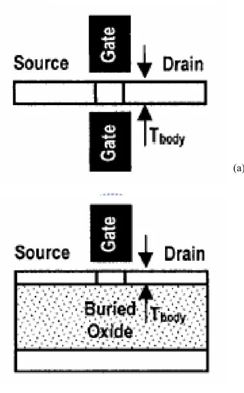
Fig. 1.2 (a) Double-Gate (DG), and (b) Ultra-Thin-Body (UTB) MOSFET structure cross-sections.
Fig. 1.3 Using a single gate material for both NMOS and PMOS devices can yield symmetric but large threshold voltages. Achieving low and symmetric threshold voltages will require two different midgap gate materials.
Chapter 2
Fig. 2.1 Cross sections illustrating the dual-metal gate process, after etching TiN/Ti and before deposition of Mo and TiN (top), and after the gate etch and source-drain implantation to show the gate stack (bottom).
Fig. 2.2 Schematic illustration of the process flow. (a) CMOS structure after second metal has been removed from the n-MOS side. (b) CMOS structure after annealing shows that the metals on the p-MOS side have interdiffused, and second metal has segregated to the dielectric interface.
Fig. 2.3 XPS depth profile for Ti/Ni gate electrode after the 400C, 30 min interdiffusion anneal. A large concentration of Ni is present at the SiO2 interface.
Fig. 2.4 Cross-sectional view of CMOS device during processing after Mo deposition (a), and after gate etching (b).
Fig. 2.5 (a)Auger profile of As, Ni, Si, and O. Full silicidation of the n+ poly gate and
significant pile-up of As on the top of gate dielectric is evident. (b)Auger profile of B, Ni, Si, and O. Full silicidation of the p+poly gate and significant
Fig. 2.6 Work function extracted from C-V curves for various composition for Ru-Ta alloys. Non-linear behavior as a function of content is observed.
Fig. 2.7 XRD peaks of Ru-Ta alloys annealed at 900C RTA in Argon.
Chapter 3
Fig. 3.1 The detailed metal gate capacitor process flow diagram.
Chapter 4
Fig. 4.1 The work function modulation as a function of Hf power ratio in non-linear and linear behaviors.
Fig. 4.2 High frequency C-V characteristics of Hf and Mo. Fig. 4.3 The work function extractions of Hf and Mo. Fig. 4.4 XRD spectra of Hf and Mo.
Fig. 4.5 High frequency C-V characteristics of as-deposited and post 400C annealing Hf gate.
Fig. 4.6 The difference of equivalent oxide thickness as a function of annealing temperature.
Fig. 4.7 High frequency C-V characteristics of the HfxMo(1-x) alloy with 3-nm-thick ,
6-nm-thick and 8-nm-thick oxide.
Fig. 4.8 The work function extractions of HfxMo(1-x) alloy.
Fig. 4.9 The work function in the theoretical and experimental value as a function of Hf power ratio.
Fig. 4.10 XRD spectra of 50% Hf power ratio sample after high temperature annealing. Fig. 4.11 Phase diagram of Mo-Hf binary alloy.
Fig. 4.12 Hysteresis of 50% Hf power ratio sample.
Fig. 4.13 The difference of equivalent oxide thickness as a function of the Hf power ratio.
Fig. 4.14 The difference of equivalent oxide thickness as a function of annealing temperature.
Fig. 4.15 Auger depth profile of post 600C annealing 50% Hf power ratio sample.
Fig. 4.16 RBS depth profile of as-deposited and post 600C annealing 50% Hf power ration sample.
Fig. 4.17 High frequency C-V of post 400C annealing HfxMo(1-x) alloy with 3-nm-thick ,
6-nm-thick and 8-nm-thick oxide.
Fig. 4.18 The work function extractions of post 400C annealing sample.
Fig. 4.19 The work function extractions of as-deposited and post 400C annealing sample. Fig. 4.20 The work function difference as a function of post 400C annealing sample.
Chapter 1
Introduction
1.1 Background and Motivation
As MOSFET gate lengths are scaled down to 0.1um regime and the equivalent gate-oxide thickness in MOS devices are downscaled into sub-2nm region, considerable challenges are encountered for higher integrated circuit density and performance. The problems of poly-silicon gate depletion, high gate resistance, high gate tunneling leakage current, and boron penetration into the channel region become more severe as the channel length and gate-oxide thickness are aggressively reduced [1]-[3]. The poly-silicon gate depletion adds 3-5Å to the equivalent oxide thickness (EOT) of the gate dielectric, exacerbating the challenge of achieving sub–10Å EOT. High gate resistance results in larger RC time delay, so it may be a show stopper for the high speed devices. In addition, poly-silicon was found to have poor thermodynamic stability on metal-oxide dielectrics which are being investigated to replace SiO2 as the gate
dielectric [4]-[6]. Therefore, there is great interest in metal gates.
The use of metal gates can not only eliminate the inherent drawback of poly-silicon but also drastically reduce the sheet resistance of gate electrode. The early approach of metal gate technology employs single metal with mid-gap work function for both NMOSFET and
PMOSFET [7]. The drawbacks are that the threshold voltages would be too large to be applied to low voltage-low power applications. Counter channel doping can lower the threshold voltage while the short-channel and turn-off characteristics will be degraded. Therefore, an approach analogous to the established dual-poly-silicon gate technology, i.e., a dual-metal gate technology, would be preferred. For bulk CMOS devices, metals with work functions (Φm)
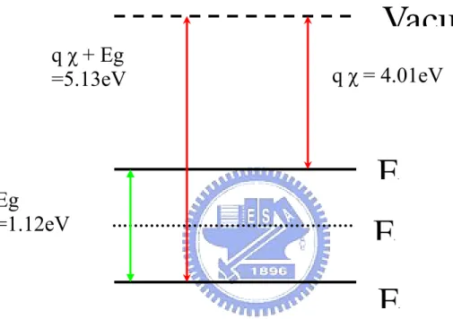
near the silicon conduction and valence band edges, i.e., ~4eV and ~5.1eV, are needed for NMOS and PMOS devices, respectively (Fig. 1.1) [8].
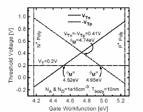
When device scales down to the physical limit, new structures will be necessary such as the symmetric double-gate (DG) MOSFET, FinFET and/or ultra-thin body (UTB) MOSFET shown in Fig. 1.2. The gate controlling ability to the channel for the new structures are better than the conventional bulk MOSFET. The required work function for the new device structures would not be ~4eV or ~5eV [9]. As shown in Fig. 1.3, to achieve low and symmetric threshold voltage, the required work functions for N- and P-channel devices will be increased and decreased, respectively, compared to those for bulk devices. It is also worth to note that the values of required metal work functions depend on body thickness. Therefore, the required metal work functions would be about 4.4 ~ 4.6 eV and 4.8 ~ 5.0 eV for N- and P-channel devices, respectively.
In this work, we propose dual work function metal gate technology using the binary metallic alloys HfxMo(1-x). Linear work function modulation of binary alloys could be achieved.
For bulk MOSFET, dual metal gates with Hf0.75Mo0.25 (~ 4.15 eV) and Mo (~ 4.95 eV) are
applied to NMOS and PMOS devices to replace poly-silicon gates. For nanometer devices, body thickness variation results in the threshold voltage shift. We require adjustable work function to optimize threshold voltage for low power operation. Linear work function modulation using HfxMo(1-x) binary metallic alloys can solve this problems.
1.2 Organization of the Thesis
The dissertation is divided into five chapters.
In chapter 2, we review some metal gate technologies and discuss their advantages and drawbacks. Midgap work function of TiN, dual work function metal gate using Ti and Mo, dual work function by Ni-Ti interdiffusion, work function adjustment of the single metal gate by nitrogen implantation, work function adjustment of the single metal gate by full silicidation and adjustable metal work function of binary metallic alloys are introduced.
In chapter 3, the detailed process flow will be described such as LOCOS isolation, gate oxide growth, metal gate deposition by co-sputtering, electrical characteristics measurement, and material analysis. The method of metal work function extraction will also be illustrated. Chapter 4 focuses on electrical characteristics and thermal stability of Hf or Mo single metal and Hf-Mo binary alloy gates. Different RTA conditions are performed to estimate the thermal stability. The results of the material analysis such as X-ray Diffraction Analysis (XRD),
Rutherford Backscattering Spectrometer (RBS), and Auger Electron Spectrometer (AES) are also shown.
Chapter 2
Review of Atate-of-the-Art Metal Gate Technology
2.1 Several approaches to the metal gate process
Here, we introduce several approaches to the metal gate process such as mid-gap work
function of TiN gate, dual work function metal gate using Ti and Mo, dual work function by Ni-Ti interdiffusion, work function adjustment of the single metal gate by nitrogen implantation, work function adjustment of the single metal gate by full silicidation, and adjustable metal work function of binary metallic alloys.
2.1.1 Mid-gap Work Function of TiN gate
In order to eliminate the poly depletion we choose metal gates to replace poly-silicon gates. TiN gate was applied to the CMOS technology. When CMOS devices used TiN as metal gate, symmetric threshold voltages were attained due to its mid-gap work function but the values were too large for low-voltage operation. Therefore, in view of the device performance and scaling, dual work function metal gate technology would be preferable to single metal with mid-gap work function.
2.1.2 Dual Work Function Metal Gate Using Ti and Mo
A straightforward way to implement a dual-work function metal gate CMOS technology is shows in Fig. 2.1. Where Ti metal gate is used in the NMOS region and Mo metal gate is used in the PMOS region. After blanket deposition, the first metal Ti (Φm ~4eV) is removed with a
RCA solution (NH4OH:H2O2:H2O mixed in the proportion of 1:2:5) from the PMOS region and
then a second metal Mo (Φm ~5eV) with a different work function is deposited [10].
Unfortunately, this entails exposing the gate dielectric to the metal etchant, which causes undesirable thinning and potential dielectric reliability problems.
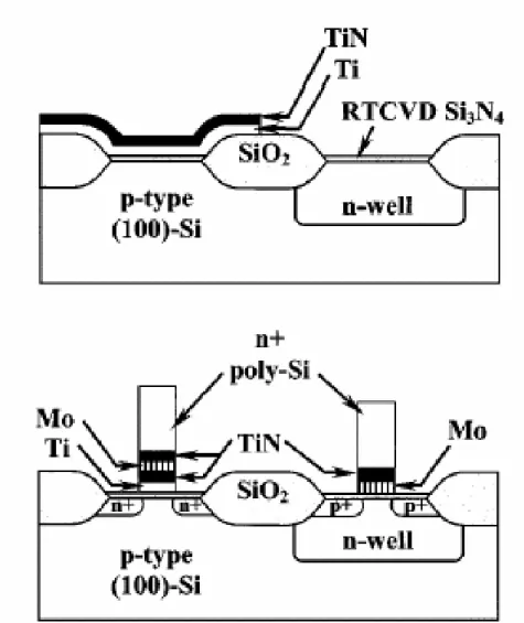
2.1.3 Dual Work Function by Ni-Ti interdiffsion
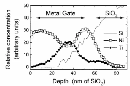
Alternative approach is proposed that the dual work function gates can be fabricated without exposing the gate dielectric to the metal etchant [11]-[12]. First, a thin layer of Ti (Φm
~3.9eV)was deposited over the entire wafer; then Ni was deposited over the entire wafer. Ni (Φm ~5eV) was then selectively removed from the NMOS region while the PMOS regions are
protected by photoresist (Fig. 2.2). Since the low work function metal Ti is the only metal remaining metals on top of the NMOS dielectric, it will clearly determine the NMOSFET threshold voltage. A 400℃ anneal was then applied in order to interdiffuse the Ti and Ni layers in the PMOS region. Due to the high diffusivity of Ni in Ti, this low thermal budget is sufficient to ensure that Ni diffuses through the Ti layer to the dielectric interface. Fig. 2.3 shows that Ni
has diffused to SiO2 interface. It is a pity that the higher gate leakage current seen in the PMOS
device is likely due to Ti reaction with the gate oxide during the interdiffusion anneal. It can not be applied to conventional CMOS technology because the thermal stability is poor.
2.1.4 Work Function Adjustment of the Single Metal Gate by Nitrogen Implantation
Except for the above two approaches to obtaining the dual work function, one can also use a single metal gate material for both NMOSFET and PMOSFET while still enabling separate work function control. Here we introduce two methods of adjustable work function for the single metal gate. One is the use of nitrogen implantation, and the other is the full silicidation of poly-silicon gate.
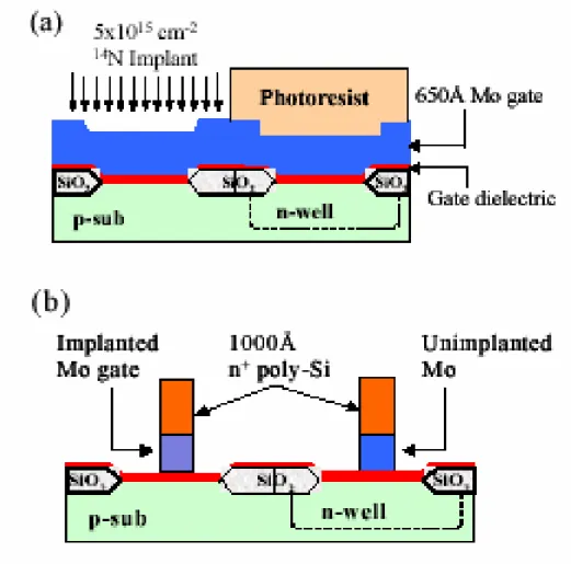
The implementation of this single metal gate concept requires a viable gate work function adjustment technique. Recently, Mo has been demonstrated as a gate metal for PMOSFET, compatible with several post-SiO2 gate dielectrics [13]. It has also been shown that the work
function of Mo can be modulated by nitrogen implantation [14]. An n-well CMOS process with LOCOS isolation was used. Gate SiO2 deposition was followed by sputter deposition of 650Å
Mo. The PMOSFET were then masked with photoresist while NMOSFET gates received a nitrogen implant (dose 5x1015 cm-2, energy 29keV). Fig. 2.4 shows the cross-sectional view of
CMOS device processes [15]. A gate work function reduction of 0.42eV was achieved for the NMOSFET. However, the magnitude of work function modulation is not large enough [16]. For
the ultra thin body application, the threshold voltage of NMOSFET will still be too large.
2.1.5 Work Function Adjustment of the Single Metal Gate by Full Silicidation
Self-aligned silicide (SALICIDE) technology has been used in advanced CMOS process [17], in which only partial poly-silicon gets silicided. The extension of existing SALICIDE technology into fully silicided gates has several advantages from a processing point of view, and its low temperature formation is CMOS compatible. Thick oxide capacitor data with fully silicided poly-silicon gates has been recently reported for NiSi where two different work functions were found for n+ and p+ poly [18]. Conventional CMOS transistors with 1.7nm
equivalent oxide thickness nitride/oxide dielectric stack and poly-silicon gates were built. No channel doping was utilized. Poly-silicon gates were doped with B and As for PMOS and NMOS, respectively. From electrical results, it is estimated that NMOS work function is ~4.5eV and PMOS ~4.9eV. The change of metal work function in NMOS side may be attributed to As piled-up at the top of gate dielectric interface. In PMOS region, there is much less of B accumulation at the gate dielectric/electrode interface (Fig. 2.5). For the NMOSFET, the work function is still too large to obtain low threshold voltage, and the channel doping will still be needed for threshold voltage control.
Recently, metal alloys were proposed for work function modulation [19]-[20]. Binary metallic alloys of Ru and Ta have been proposed as candidates for CMOS gate electrodes. RuxTay films were co-sputtered on thermal grown SiO2 from Ru and Ta targets. The sputtering
power of Ta and Ru was varied to modulate the composition. Fig. 2.6 shows the work function extraction for various compositions of RuxTay alloys. Non-linear work function modulation
behavior is observed. New alloy phase forms (Ta content between 40% and 64%) and results in the Φm dropping abruptly (Fig. 2.7). The work functions between 4.6eV and 4.9eV needed for
FinFET and/or UTB-SOI devices may not be available.
For reasons mentioned above, dual work function is essential for advanced CMOS techniques. In this work, we choose the binary metallic alloys to replace the conventional poly-silicon gate. The linear work function modulation using binary metallic alloys of Hf and Mo have been achieved successfully, and it will be discussed particularly later.
2.2 Metal Film Deposition with the Sputter System
There are two methods to deposit the metal film by using chemical vapor deposition (CVD) and physical vapor deposition (PVD). Take TiN gate for example, CVD-TiN prepared by metalorganic precursors introduced high carbon impurity and reliability problems, while the film by TiCl4 and NH3 generated unstable capacitance equivalent thickness variation and
electrode is favorable than Chemical Vapor Deposition, because the impurity contained in the metal deposited by CVD may degrade the gate dielectric reliability during high temperature annealing processes. Sputtering is a term used to describe the mechanism in which atoms are ejected from the surface of a material when that surface is struck by sufficiently energetic particles. It has become the dominant technique for depositing a variety of metallic films in VLSI and ULSI fabrication. In our experiment, the binary alloy films are deposited by co-sputtering. The DC power applied into the target is modulated to vary the composition of binary metallic alloys. Different contents of Hf and Mo in the binary metallic alloys will result in dissimilar work function values.
2.3 Gate Last Technology-Replacement and Damascene Gate Process
In conventional metal gate designs, the source/drain annealing temperature must be limited to prevent degradation of the gate insulator integrity and metal film stability. It is well-known that the metal gates are easily degraded by high temperature process in term of structural stability, moreover, underneath gate oxide is more susceptible to plasma charging damage originated in the source/drain implantation and the gate reactive ion (RIE) processed. The replacement gate design has the unique advantage that the annealing of the source/drain implants is performed prior to the gate insulator formation. Therefore, annealing temperatures higher than 1000 ℃ can be employed to fully active the source/drain dopants without thermal
stability concerning, and the processing temperature after gate formation can be further reduced to as low as 400 ℃.
The replacement gate process was proposed to employ the low resistance and depletion-free properties of metal gates in trying to achieve superior high-speed transistors. In this processes, poly-silicon dummy gates are replaced by metal gate after high temperature process for source/drain activation. However, this process is suffering some drawbacks of complexity and compatibility. For example, these metal gate should be patterned by an additional lithography and defined by using the reactive ion etching (RIE) process as T-shape gate, requiring some difficult process step for the precise mask alignment of the metal gate to the dummy gate and the plug to the metal gate.
On the other hand, in order to overcome the incurring complexity in replacement gate process, metal wiring can be fabricated by chemical mechanical polishing (CMP), which is widely used in multilevel interconnection. This type of metal wiring process utilizing CMP is referred to as the damascene process. This novel gate formation process can further prevent deteriorating the gate electrodes and the gate oxides reliability from the plasma and thermal damage.
In the damascene process, the gate insulator and gate electrodes are deposited after ion implantation and high temperature annealing (about 1000 ℃) for source/drain formation, and then the gate electrodes are fabricated by CMP of gate material deposited in grooves. Metal
gates and high dielectric constant gate insulators are applicable to the MOSFET, since the processing temperature after gate formation can be much lower than those in conventional CMOS processes. The process damage on gate insulators can also be minimized because there is no plasma-related process involved.
Chapter 3
Experiments and Measurements
3.1 Process Flow of the Binary Metallic Alloys Gated Capacitor
The binary metallic alloys gated capacitors were fabricated on 6-inch p-type (100) 15 - 25 Ω-cm silicon wafers. The detailed fabrication process steps are described as follows and the process flow chart is shown in Table 3.1. The detailed process flow diagram is shown in Fig.
3.1.
● Zero mark alignment: An initial alignment key was formed at wafer surface for each mask alignment afterward.
● LOCOS isolation: A wafer with a bare silicon surface was cleaned and a 35 nm oxide was thermally grown in the horizontal furnace at 950 ℃ on the surface. The function of this layer, called a pad or buffer oxide, was to cushion the transition of stresses between the silicon substrate and the subsequently deposited nitride. Next, a 150 nm thick layer of LPCVD silicon nitride at 780 ℃ which functions as an oxidation mask was deposited. Silicon nitride was effective in this role because oxygen and water vapor diffused very slowly through it, preventing oxidizing species from reaching the silicon surface under the nitride. In addition, the nitride itself oxidized very slowly as the field oxide was grown. The active regions were now
defined with a photolithographic step. A photoresist pattern is normally used to protect all of the areas where active devices would be formed. The nitride layer was etched by TEL 5000, and then the photoresist was stripped. After active regions definition, the field oxide 550 nm was thermally grown by means of wet oxidation at 980 ℃. Following field oxidation, the masking layer was removed. Since 20-30 nm of the top of the nitride was converted to SiO2 during the
field oxidation, this layer must be etched off first by BOE dipping for 15 seconds. The remaining nitride and pad oxide were then etched. Nitride was removed by H3PO4 at 165 ℃ for
65 minutes and pad oxide was removed by HF. A 35 nm sacrificial oxide was grown at 925 ℃ to remove any dry-etch induced damage or unwanted nitride. And then, using the HF solution removed the sacrificial oxide. Finally, sacrificial oxide was grown again to protect the active region before gate oxide growing.
● Gate oxide deposition: First, sacrificial oxide was removed using HF-dip and gate oxide was thermally grown by dry oxidation using the vertical furnace at 800 ℃. To decouple the contribution of fixed charge, three different oxide thicknesses, i.e., 3 nm, 6 nm, and 8 nm were deposited.
● Metal Gate deposition: After the growth of gate oxide, metal films were deposited on the top of it. Two control samples gated by single metal were fabricated. One was gated by 50 nm pure Hf and the other was gated by 50 nm pure Mo. On the other hand, samples gated by binary metallic alloy HfxMo(1-x) were also fabricated. The HfxMo(1-x) films were deposited by
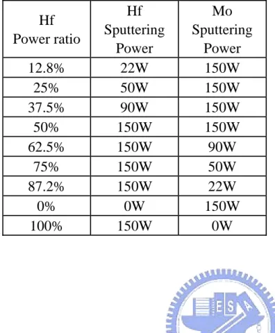
co-sputtering with 50 nm thickness. The sputtering power was modulated to vary the composition of binary metallic alloys (List in Table 3.2). The gate electrodes were then patterned by reactive ion etching (RIE) using Cl2 based chemistry.
● Metal Rapid Thermal Anneal: Samples were then subjected to different RTA conditions from 400 ℃ to 1000 ℃ for 30 seconds to evaluate the possible thermal cycle in conventional CMOS process.
3.2 Measurement Techniques
In this section, the characteristics of the devices were performed on metal gate capacitor test devices using an HP 4284 capacitance-voltage measurement system and KEITHLEY 4200.
3.2.1 Thickness Measurement of Ultra-Thin Gate Oxide
Two techniques were used to determine the physical gate oxide thickness, one is ellipsometer and the other is n & k analyzer. Before n & k analyzer measurement, a baseline wafer is used to calibrate. Some thin oxide may be formed on the baseline wafer for a long time. When the thin film we wanted to measure is thinner than the oxide on the baseline wafer, we can not know the thickness because the value is zero. Ultra-thin films under 10 nm had better be measured with ellipsometer. The film over 10 nm is often measured with n & k analyzer. Therefore, the physical oxide thickness was determined by ellipsometer in our experiment.
3.2.2 Capacitance-Voltage Measurement
The C-V techniques can be used to analyze process, product and reliability, etc. We can benefit from C-V data, such as equivalent oxide thickness and capacitance, etc. We can estimate the flat-band capacitor from C-V data, and then find out the flat-band voltage VFB. In the C-V
theory, the flat-band capacitance is expressed as:
( ) ( )( ) ox FB ox s ox s C kT t e eNa ε ε ε ε = +
where tox is the effective oxide thickness, Na is the substrate doping, and εox andεs are the
dielectric constant of oxide and silicon substrate, respectively. From effective oxide thickness and flat-band voltage, the metal gate work function can be extracted. In our experiment, the flat-band voltage and effective oxide thickness may vary due to the different thermal treatment. The capacitance of the metal gate capacitor may increase or decrease and the flat-band voltage may shift under high temperature annealing. The C-V measurement is a powerful tool to inspect those changes in capacitances and the flat band voltage shift.
3.2.3 X-ray Diffraction Analysis (XRD)
The microstructure of metal film is examined by XRD. The specimen is mounted in the center of the diffractometer and rotated by an angle θ around an axis in the film place. The counter is attached to an arm rotating around the same axis by angles 2θ twice as large as
by shrink with increasing diffraction angle. Only (hkl) plans parallel to the film place contribute to the diffraction from the pattern of specific diffraction peak, the crystalline of films can be characterized.
3.2.4 Auger Electron Spectrometer (AES)
Auger electron spectrometer techniques can be used to analyze the depth distribution of the concentration of the composite elements in the sample from surface to inner. The analyst excited the auger electrons by electronic beams and the same time sputtered the sample by ionic beams to generate the new surface of the sample. From the auger electron spectroscopy, the concentration of the composite elements in different depth can be attained.
3.2.5 Rutherford Backscattering Spectrometer (RBS)
Rutherford backscattering spectrometer uses low energy α particle (2 – 3 MeV) to bombard the device under test. The α particle is generated by Van de Graaff Accelerator. The surface barrier semiconductor detector collected scattering α particle and sent to the amplifier and multiple channel analyzer and finally analyzed by the personal computer. From RBS, the composition and percentage of elements can be attained.
There are two methods to extract the metal gate work function. One is comparing the flat-band voltage shift between metal gate devices and that with known work function value such as n+ poly-silicon in the same process runs. From the known work function of n+
poly-silicon and flat-band voltage difference between n+ poly-silicon and metal, the metal work
function can be estimated. But the value of the work function is less precise. The other approach bases on the expression of flat-band voltage:
i FB MS ox ox Q V t ε = Φ −
where Qi is the density of fixed oxide charges, εox is the dielectric constant of the oxide, and tox
is the thickness of oxide. In order to decouple the effect of fixed oxide charge from the work function, C-V measurement on several oxide thickness were used to generate a VFB vs. EOT
curve. The y-intercept of this curve indicated the ΦMS value. Since Qi must be constant in order
to obtain meaningful values for ΦMS, we have prepared different oxides on the same wafer to
ensure that Qi is the same. This method is more precise than the earlier one so in our calculation the second method is used.
Chapter 4
Characteristics and Thermal Stability of Hf and Mo
Single and Binary Alloy Gate
4.1 Introduction
As MOS technology scales toward sub-0.1um regime, the poly-silicon gate depletion effect, caused by insufficient dopant activation near the poly-silicon/SiO2 interface, becomes
increasingly intolerable. To overcome this problem, the replacement of conventional poly-silicon gate by refractory metals, such as TiN or WN, has recently been proposed [24]-[25]. However, the use of metal gate itself could create many new issues such as process compatibility, metal penetration, and threshold voltage variation, etc. More efforts are thus required to improve the control of the processes as well as the device performance. In order to optimize threshold voltages in high performance devices, the metal gate need tunable work function for NMOS and PMOS devices in CMOS process similar to present poly-silicon gate technology. When transistor scales down to the physical limit, new structures will be necessary such as the symmetric double-gate (DG) MOSFET, FinFET and/or ultra-thin body (UTB) MOSFET. The required work function for the new device structures would not be ~4eV or ~5eV. To achieve low and symmetric threshold voltage, the required work functions for N- and
P-channel devices will be increased and decreased, respectively, compared to those for bulk devices. It is also worth to note that the values of required metal work functions depend on body thickness. Therefore, the required metal work functions would be about 4.4 ~ 4.6 eV and 4.8 ~ 5.0 eV for N- and P-channel devices, respectively.
This study investigated the metal gate work function modulation using binary metallic alloys HfxMo(1-x) on the NMOS capacitor. Rapid thermal anneal (RTA) was employed in this
work to estimate the thermal stability of the binary metallic alloys HfxMo(1-x). Impact of the
high-temperature treatment on gate oxide was characterized and discussed.
4.2 Experimental Procedures
NMOS capacitors with Hf or Mo single metal and Hf-Mo binary alloy gate electrodes were fabricated on 6-in. p-type silicon wafers with conventional LOCOS isolation process. Briefly, three oxide thickness (3 nm, 6 nm , and 8 nm) were grown in the vertical furnace at 800 ℃, followed by the gate electrodes deposition. 50-nm-thick single metal films HfxMo(1-x) were
deposited by sputtering and 50-nm-thick binary metallic alloys films of Hf and Mo deposited by co-sputtering in argon ambient. Here, the sputtering power of Hf and Mo were split into nine conditions as shown in Table 4.2. Gate electrodes of all samples were etched in a Cl2-based
helicon-type plasma etcher, followed by photoresist stripping in a down-stream O2 plasma asher.
Specifically, the annealing conditions are 400 –1000 ℃ for 30 seconds.
4.3 The Work Function of Binary Metallic Alloys System
We first introduce the approximate equation of the binary metallic alloys proposed by AgAu [24]. The work function of an AxB1-x alloy can be approximately expressed as
( , , )( ) , (1 ) , (1 )[ (1 ) m A m B A B m m A m B A B x x x x x x ] ρ ρ ρ ρ Φ −Φ − Φ = Φ + − Φ + − + − ( , , )( 1) , (1 ) , (1 )[ (1 ) A m A m B B m A m B A B x x x x x x ] ρ ρ ρ ρ Φ −Φ − = Φ + − Φ + − + −
where Φm,A and Φm,B are the work functions of pure A and B metals, respectively, and ρA and ρB
are the Fermi-level density of states. The density of states at Fermi energy ρ(εF) is proportional
to electronic specific heat constant 1 2 2
( )
3 F B
Ce= π ρ ε k T =γT [25], where kB is Boltzmen
constant, T is temperature, and γ is called Sommerfeld parameter. The electronic term is linear in T and is dominant at sufficiently low temperatures. Therefore, we can obtain A
B B A
ρ γ
ρ =γ . In the caes of ρA / ρB ~1, the Φm changes with x linearly as Φm = Φx m A, + − Φ(1 x) m B, . The γ values of Hf and Mo are about 2.16 and 2.0 mJ/mole/K2, respectively. Since the γ values of Hf and Mo
are very close, a nearly linear work function modulation can be expected. Fig. 4.1 shows the comparison between non-linear with linear behavior on work function modulation. Linear work function modulation is a compromise between modulation efficiency and immunity to process variation.
4.4 Characteristics and Thermal Stability of Hf and Mo Single Gate
Fig. 4.2 shows the C-V characteristic of as-deposited Hf and Mo single metal gated capacitors. Fig. 4.3 shows the wok function extraction of Hf and Mo. We use work function extraction to obtain the work function of Hf is 3.95eV and the work function of Mo is 4.95eV. XRD spectra of Hf and Mo are shown in Fig. 4.4. From XRD figures, we can find the peak corresponding the metal phase from the JCPDS information. Comparing work function values of Hf and Mo extracted in this work with reported data, good agreement was obtained.
It seems that Hf and Mo can be applied to dual work function metal gate technology, since work function values of Hf and Mo are suitable for gate electrodes of N- and P-MOSFET bulk devices, respectively. Unfortunately, thermal stability of Hf was found to be poor. From C-V curves, the equivalent oxide thickness of post 400℃ annealing Hf gated capacitor changes as show in Fig. 4.5. Therefore, Hf is not a good gate candidate even for gate-last process. The equivalent oxide thickness change is likely due to Hf reaction with the oxide. Because Hf has high oxygen solubility, it will form Hf-O bonds in Hf and oxide interface. By contrast, the thermal stability of Mo is excellent until 900℃ as shown in Fig. 4.6. Whether the HfxMo(1-x)
alloy provides any advantage of improvement of thermal stability will be discussed later.
4.5 Characteristics and Thermal Stability of Binary Metallic Alloys
Hf
xMo
(1-x)Fig. 4.7 shows C-V characteristics of binary metallic alloys HfxMo(1-x). The flat-band
voltage shift may be due to the variation of Hf content in Hf-Mo alloy with the sputtering power. When the ratio of the sputtering power of Hf is increased, the Hf atomic fraction in Hf-Mo alloy becomes larger. The electrical characteristic of alloy will become more Hf-like, and flat-band voltage will shift toward left. From C-V curves, we can obtain the VFB and EOT values of
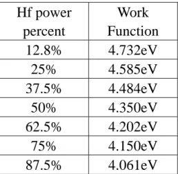
HfxMo(1-x) alloy needed for work function extraction as shown in Fig. 4.8. The extracted work
function values of HfxMo(1-x) alloys are listed in Table 4.1. Comparison between the
experimental and calculated work function values in the case of ρMo /ρHf = 0.926 is shown in
Fig. 4.9. From this figure, we can see the experimental result exhibited linear work function
modulation behavior as we expected. The difference between theoretical value and experimental value may be attributed to the deposition rate difference between Hf and Mo.
Fig. 4.10 shows the XRD spectra of 50 % Hf power ratio sample. There is no peak found
after high temperature annealing. To put it plainly the alloy film is amorphous. Fig. 4.11 shows the Mo-Hf phase diagram [26]. In our experiment, the highest annealing temperature is lower than 1000 ℃ so no specific compound will be formed, which maybe result in work function decreasing abruptly. Process quality was demonstrated in Fig. 4.12, since the 50% Hf power ratio sample suffering maximum power summation still exhibits negligible hysteresis.
Thermal annealing from 400 ℃ to 1000 ℃ for 30seconds was used to estimate the thermal stability of HfxMo(1-x) alloy. Fig. 4.13 shows the EOT variation versus Hf power ration as a
function of the annealing temperature. Experimental results were then rearranged as shown in
Fig. 4.14. It can be observed that the increase of Hf power ratio leads to larger Hf atomic
fraction in alloy and then poorer thermal stability. For example, the thermal stability of 75% Hf power ratio sample was as low as 400 ℃.
As mentioned above, the thermal stability of Hf is too low to be suitable for gate electrode candidate for bulk NMOSFET. By contrast, the Hf0.75Mo0.25 alloy have been demonstrated to
provide suitable work function value (~ 4.15 eV) and better thermal stability (up to 400 ℃) so that the combination of Hf0.75Mo0.25 / Mo may be a new candidate for dual work function metal
gate bulk CMOS technology in gate-last process.
Auger depth profiles of post 600 ℃ annealing 50% Hf power ratio sample is shown in Fig.
4.15. Uniform composition throughout the film and abrupt interface can be observed. Hf does
not pile up in oxide interfaceand no obvious metal atom penetration into gate oxide. The RBS depth profile shown in Fig. 4.16 exhibits the same result.
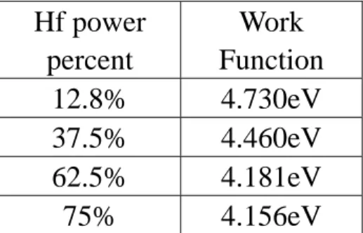
The C-V curves of post 400 ℃ annealing samples are shown in Fig. 4.17. The work function extraction from VFB-EOT figure is shown in Fig. 4.18 and extracted Φm value are
listed in Table 4.2. Fig. 4.19 shows the comparison between Φm extraction of as-deposited
samples and that of post 400 ℃ annealing samples. We can see that the work function values of HfxMo(1-x) alloys have no obvious change after 400 ℃ annealing as shown Fig. 4.20.
Φm modulation using HfxMo(1-x) exhibits nearly linear behavior. On the other hand, thermal
stabilities of HfxMo(1-x) decrease with increasing of Hf atomic fraction x. Fortunately, thermal
stabilities of HfxMo(1-x) can be still higher than 400 ℃ which may be the only thermal cycle
after gate electrode deposition in gate-last process. Therefore, this proposed linear work function modulation technique exhibits great potential on gate work function engineering.
Chapter 5
Conclusion
As gate length downscales to 0.1um region, metal gate will be highly desired to replace conventional poly-silicon gate. Binary metallic alloys using HfxMo(1-x) were studied for gate
electrode applications. Linear work function modulation using HfxMo(1-x) binary metallic alloys
was achieved successfully in our experiment. For bulk NMOSFET, the metal work function needed is 4 ~ 4.2 eV, and Hf0.75Mo0.25 (~ 4.15eV) can be used to replace n+ poly-silicon gate.
For nanometer devices such as the symmetric double-gate (DG) MOSFET, FinFET and/or ultra-thin body (UTB) MOSFET, the required metal work functions depend on the body thickness and gate numbers. Conventional threshold voltage control using channel doping will inherently lead to carrier mobility degradation. So the role of metal work function engineering will be more pronounced. Work function modulation can be distinguished into non-linear and linear behaviors. Linear work function modulation is a compromise between modulation efficiency and immunity to process variation. Linear work function modulation can be used to obtain the appropriate metal work function value for nanometer device threshold voltage control without implanting additional channel doping.
Reference:
[1] C.-Y. Lu, J. M. Sung, Howard C. Kirsch, Steven J. Hillenius, T. E. Smith, L. Manchanda, “Anomalous C-V Characteristics of Implanted Poly MOS Structure in n+/p+ Dual-Gate CMOS Technology,” IEEE Electron Device Lett., vol. 10, pp.192-194, 1989.
[2] C. Y. Wong, J. Y. -C. Sun, Y. Taur, C. S. Oh, R. Angelucci, and B. Davari, “Doping of N+ and P+ Polysilicon In A Dual-Gate CMOS Process,” IEDM Tech. Dig., pp.238-241, 1988.
[3] James R. Pfiester, Frank K. Baker, Thomas C. Mele, H. H. Tseng, Philip J. Tobin, James D. Hayden, James W. Miller, Craig D. Gunderson, Louis C. Parrillo, “The Effect of Boron Penetration on p+ Polysilicon Gated PMOS Devices,” IEEE Trans. Electron Devices, vol. 37, pp.1842-1851, 1990.
[4] H. F. Luan, B. Z. Wu, L. G. Kang, B. Y. Kim, R. Vrtis, D. Roberts, and D. L. Kwong, “Ultra thin high quality Ta2O5 gate dielectric prepared by in-situ rapid thermal processing,” IEDM
Tech. Dig. pp.609-612, 1998.
[5] C. H. Lee, H. F. Luan, W. P. Bai, S. J. Lee, T. S. Jeon, Y. Senzaki, D. Roberts, and D. L. Kwong, “MOS characteristics of ultra thin rapid thermal CVD ZrO2 and Zr silicate gate
dielectrics,” IEDM Tech. Dig. pp.27-30, 2000.
[6] Y.-C. Yeo, P. Ranade, Q. Lu, R. Lin, T.-J. King, C. Hu, “Effects of High-k Gate Dielectric Materials on Metal and Silicon Gate Workfunction,” IEEE Electron Device Lett., vol. 23, pp.342-344, 2002.
[7] B. Maiti, P. J. Tobin, . Hobbs, R. I. Hegde, F. Huang et al., “PVD TiN Metal Gate MOSFETs on Bulk Silicon and Fully Depleted Silicon–On-Insulator (FDSOI) Substrates for Deep Sub-Quarter Micro CMOS Technology,” IEDM Tech. Dig., pp781-784, 1998.
[8] I. De, D. Johri, A. Srivastava, C. M. Osburn, “Impact of gate workfunction on device performance at the 50nm technology node,” Solid-State-Electronics, vol. 44, pp.1077-1080, 2000.
[9] L. Chang, S. Tang, T.-J. King, J. Boker, C. Hu, “Gate Length Scaling and Threshold Voltage Control of Double-Gate MOSFETs,” IEDM Tech. Dig., pp.719-722, 2000.
[10] Y.-C. Yeo, Q. Lu, P. Ranade, H. Takeuchi, C. Hu et al., “Dual-Metal Gate CMOS Technology with Ultrathin Silicon Nitride Gate Dielectric,” IEEE Electron Device Lett., vol. 22 , pp.227-229, 2001.
[11] I. Polishchuk, P. Ranade, T. J. King, C. Hu, “Dual Work Function Metal Gate CMOS Technology Using Metal Interdiffusion,” IEEE Electron Device Lett., vol. 22, pp.444-446, 2001.
[12] I. Polishchuk, P. Ranade, T. J. King, C. Hu, “Dual Work Function Metal Gate CMOS Transistors Fabricated by Ni-Ti Interdiffusion,” Symp. on Semiconductor Device Research, pp.411-414, 2001.
[13] Q. Lu, R. Lin, P. Ranade, Y.-C. Yeo, C. Hu et al., “Molybdenum Metal Gate MOS Technology for Post-SiO2 Gate dielectrics,” IEDM Tech. Dig., pp.641-644, 2000.
[14] P. Ranade, Y. C. Yeo, Q. Lu, C. Hu, “Molybdeum as a gate electrode for deep sub-micro CMOS technology,” MRS Symp. Proc., vol. 611, San Francisco, CA, Spring 2000.
[15] Q. Lu, R. Lin, P. Ranade, T. J. King, C. Hu, “Metal Gate Work Function Adjustment for Future CMOS Technology,” Symp. on VLSI Tech., pp.45-46, 2001.
[16] R. Lin, Q. Lu, P. Ranade, T. J. King, C. Hu, “An Adjustable Work Function Technology Using Mo Gate for CMOS Devices,” IEEE Electron Device Lett., vol. 23, pp.49-51, 2002. [17] T. Morimoto, H. S. Momose, T. Iinuma, I. Kunishima et al., “A NiSi Salicide Technology for Advanced Logic Devices,” IEDM Tech. Dig., pp.653-656, 1991.
[18] W. P. Maszara, Z. Krivokapic, P. King, J.-S. Goo and M.-R. Lin, “Transistors with Dual Work Function Metal Gates by Single Full Silicidation (FUSI) of Polysilicon Gates,” IEDM Tech. Dig., pp.367-370, 2002.
[19] H. Zhong, S.-N. Hong, Y.-S. Suh, H. Lazar, G. Heuss and V. Misra, “Properties of Ru-Ta Alloys as Gate Electrodes For NMOS and PMOS Silicon Devices,” IEDM Tech. Dig., pp.432-435., 2001.
[20] D.-G. Park, T.-H. Cha, K.-Y. Lim, H.-J. Cho et al., “Robust Ternary Metal Gate Electrodes for Dual Gate CMOS Devices,” IEDM Tech. Dig., pp.671-674, 2001.
[21] D.-G Park, K.-Y. Lim, H.-J. Cho, T.-H Cha, I.-S Yeo, J.-S Roh, and Jin Won Park, “Impact of atomic-layer-deposited TiN on the gate oxide quality od W/TiN/SiO2/Si metal-oxide-semiconductor structures,” Appl. Phys. Lett., pp.2514-2516, 2002.
[22] T. Ushiki, K. Kawai, I. Ohshima and T. Ohmi, “Chemical reaction concerns of gate metal with gate dielectric in Ta gate MOS devices: An effect of self-sealing barrier configuration interposed between Ta and SiO2,” IEEE Trans. Electron Devices, pp.2201, 2000
[23] T. Yamada , M. Moriwaki, Y. Harada, S. Fujii and K. Eriguchi, “The metal gate MOS reliability with the improved sputtering process for gate electrode,” IDEM Tech. Dig., pp.319-322, 1999
[24] C. D. Gelatt, Jr and H. Ehrenreich, “Charge transfer in alloy: AgAu,” Phys. Rev. B, pp.398-415, 1974.
[25] C. Kittel, Introduction to Solid State Physics, 7th ed. New York:Wiley,1976, pp.151-157.
[26] B. Thaddeus, Binary Alloy Phase Diagrams, 2nd ed. American Society for Metals,
Table 3.1 MOS capacitor Fabrication Process.
◎ Isolation (Fox=550 nm)
◎ SiO2 formation at 3 nm ,6 nm and 8nm
◎ Hf or Mo (50 nm) deposition by sputtering
Hf
xMo
(1-x)deposition (50 nm) by co-sputtering
◎ Electrode pattering
Table 3.2 List of Power conditions.
Hf
Power ratio
Hf
Sputtering
Power
Mo
Sputtering
Power
12.8% 22W 150W
25% 50W 150W
37.5% 90W 150W
50% 150W 150W
62.5% 150W 90W
75% 150W 50W
87.2% 150W 22W
0% 0W
150W
100% 150W 0W
Table 4.1 The work function extraction of as-deposited Hf
xMo
(1-x)alloy.
Hf power
percent
Work
Function
12.8% 4.732eV
25% 4.585eV
37.5% 4.484eV
50% 4.350eV
62.5% 4.202eV
75% 4.150eV
87.5% 4.061eV
Table 4.2 The work function extraction of post 400C annealing Hf
xMo
(1-x)alloy.
Hf power
percent
Work
Function
12.8% 4.730eV
37.5% 4.460eV
62.5% 4.181eV
75% 4.156eV
Vacu
E
E
q χ + Eg
=5.13eV
Eg
=1.12eV
q χ = 4.01eV
E
(a)
(b)
Fig. 1.2 (a)Double-Gate (DG), and (b) Ultra-Thin-Body (UTB) MOSFET
structure cross-sections.
Fig. 1.3 Using a single gate material for both NMOS and PMOS devices can yield
symmetric but large threshold voltages. Achieving low and symmetric threshold
voltages will require two different midgap gate materials.
Fig. 2.1 Cross sections illustrating the dual-metal gate process, after etching
TiN/Ti and before deposition of Mo and TiN (top), and after the gate etch and
source-drain implantation to show the gate stack (bottom).
Fig. 2.2 Schematic illustration of the process flow. (a) CMOS structure after
second metal has been removed from the n-MOS side. (b) CMOS structure after
annealing shows that the metals on the p-MOS side have interdiffused, and
second metal has segregated to the dielectric interface.
Fig. 2.3 XPS depth profile for Ti/Ni gate electrode after the 400C, 30 min
interdiffusion anneal. A large concentration of Ni is present at the SiO
2interface.
Fig. 2.4 Cross-sectional view of CMOS device during processing after Mo
deposition (a), and after gate etching (b).
(a)
(b)
Fig. 2.5 (a)Auger profile of As, Ni, Si, and O. Full silicidation of the n
+poly gate
and significant pile-up of As on the top of gate dielectric is evident. (b)Auger
profile of B, Ni, Si, and O. Full silicidation of the p
+poly gate and significant
pile-up of B on the top of gate dielectric is evident.
Fig. 2.6 Work function extracted from C-V curves for various composition for
Ru-Ta alloys. Non-linear behavior as a function of content is observed.
Standard RCA Clean
P-type substratePad oxide and nitride grow
P-type substrate
Nitride Pad oxide
Define active region and
remove nitride and pad oxide
P-type substrate
LOCOS formation
P-type substrate
P-type substrate
Remove nitride and pad oxide
Gate oxide fabrication
(3nm, 6nm, 9nm)
P-type substrate
Single metal film deposition
and gate
Binary alloy film deposition
and gate patterned
patterned
Fig. 4.1 The work function modulation as a function of Hf power ratio in
non-linear and linear behaviors.
Fig. 4.5 High frequency C-V characteristics of as-deposited and post 400C
annealing Hf gate.
Fig. 4.6 The difference of equivalent oxide thickness as a function of annealing
temperature.
Fig. 4.9 The work function in the theoretical and experimental value as a function
of Hf power ratio.
Fig. 4.10 XRD spectra of 50% Hf power ratio sample after high temperature
annealing
.Hf-Mo alloy 50%
Fig. 4.13 The difference of equivalent oxide thickness as a function of the Hf
power ratio.
Fig. 4.14 The difference of equivalent oxide thickness as a function of annealing
temperature.
Fig. 4.16 RBS depth profile of as-deposited and post 600C annealing 50% Hf
power ration sample.
400C anneal