國立交通大學
National Chiao Tung University
博士論文
Doctoral Dissertation
複雜氧化物介面交互作用之控制
Controlling the Interaction in Complex Oxide Interfaces
系 所 :
Institute of Physics
學 號 :
9727806
姓 名 :
VU THANH TRA
指導教授 :
Prof. JIUNN YUAN LIN
共同指導教授 :
Prof. YING HAO CHU
複雜氧化物介面交互作用之控制
Controlling the Interaction in Complex Oxide Interfaces
姓 名 :
武卿亞
Student: Vu Thanh Tra
指導教授 :
林俊源
Advisor: Prof. Jiunn Yuan Lin
共同指導教授 : 朱英豪
Co- Advisor: Prof. Ying Hao Chu
國立交通大學
物理研究所
博士論文
A Thesis
Submitted to Institute of Physics
College of Science
National Chiao Tung University
In partial Fulfillment of the Requirements
for the Degree of
Doctor
in
Physics
June 2013
I
Abstract
In this thesis, we investigated control the interactions of complex oxide interfaces. Hetero-interfaces between complex oxides have sparked considerable interest due to their fascinating physical properties and offer new possibilities for next-generation electronic devices. While most studies are aiming at exploring new interfaces by combining different materials, another key to realizing the practical applications is the control through external stimulus. As the first subject, we propose a generic approach to use an additional layer, e.g. ferroelectric Pb(Zr0.2Ti0.8)O3, on LaAlO3 (LAO)/SrTiO3
(STO) interface as a nonvolatile modulation of the conduction behaviors at this interface. In order to reveal the insight, the change of the interface band structure was comprehensively investigated by a combination of the ferroelectric pattern assisted x-ray photoelectron spectroscopy and scanning tunneling spectroscopy. This study opens an avenue to the nonvolatile control of complex oxide interfaces.
Moreover, in strongly correlated oxides, heterointerfaces provide a powerful route to manipulate the charge, spin, orbital, and lattice degrees of freedom to create new
functionalities. As the second part of study, the ferromagnetic (F)
La2/3Ca1/3MnO3(LCMO)/superconducting (S) YBa2Cu3O7-x (YBCO) heterostructures
of two distinct interfaces with atomically precise interface control have been fabricated to explore the interactions between these two functional layers. A new mechanism of charge transfer in these heterostructures was identified. This charge transfer, in addition to the previously considered F/S proximate effect, is critical to the superconductivity, magnetism, and x-ray absorption spectroscopy observed in these heterostructures.
Acknowledgment
This thesis presents the summary of my research work conducted in the Department of Materials Science and Engineering, and Institute of Physics at National Chiao Tung University. I would like to express my sincere gratitude to all the people who helped me during my study.
First and foremost I would like to thank my supervisors, Prof. Jiunn Yuan. Lin and Prof. Ying Hao Chu, for their patient and insightful guidance without which I could not have completed this thesis. My thanks go to the entire Smart Group and Quantum Matter physics groups in National Chiao Tung University, in particular the kind support and help during the experimental work from Prof. Chung Lin Wu, and Prof. Chen Yi Chen’ groups in National Cheng Kung University; Prof. Chiu Ya Ping’s group in National Sun Yat Sen University; Prof. Chiu Po Wen’s Group in National Tsing Hua University, Prof. Lin Hong Ji’s group in National Synchrotron Radiation Research Center, Taiwan. I would also like to thank all my friends in the groups for the morale and academic support throughout this work; Especially Dr. Heng-Jui Liu, Dr. Virendra Kumar Verma, Mr. Jang - Jan Chi, Mr. Jhih - Wei Chen, Mr. Yu – Chen Lun, and Mr. Chao-Hui Yeh.
I am grateful to the financial support from the National Science Council of Republic of China (under contract no. NSC-101-2119-M-009-003-MY2), the Ministry of Education (under grant no. MOE-ATU 101W961), and the Center for Interdisciplinary Science at National Chiao Tung University and National Chiao Tung University, especially kindly support from Prof. Jenh-Yih Juang in Department of Electrophysics, National Chiao Tung University for my international conferences trips My gratitude and thanks are extended to all of my staffs of Institute of Physics and Office of International Affairs (OIA) for dealing with matters such as admission & enrollment registration for International Research Students, an arrival orientation, arrangements of scholarships, housing, visas and organizing various intercultural events.
I would also like to thank the family members of foreign student association – National Chiao Tung University (FSA-NCTU) and Vietnamese student association – National Chiao Tung University (VSA-NCTU) who made my days at National Chiao Tung University really enjoyable and cheerful.
III
I would like to thank the whole National Chiao Tung University family which made my stay in University and Taiwan a memorable one.
My thanks also go to all those who have played the great sport of Tennis and Badminton with me at National Chiao Tung University.
Finally, I would like to thank my parents and my wife, for their tremendous support, encouragement and kindness
List of Publications
1. C. Y. Wu, V. T. Tra, Y. F. Chen, J. K. Lee, and J. J. Lin “Free-electron-like diffusive thermopower of indium tin oxide thin films” J. Appl. Phys. 108, 123708 (2010)
2. Y. Y. Chu, Y. F. Liao, V. T. Tra, J. C. Yang, W. Z. Liu, J. Y. Lin, Y. H. Chu, J. H. Huang, J. Weinen, S. Agrestini, K. D. Tsuei, and D. J. Huang, “Distribution of Electronic Reconstruction at the n-type LaAlO3/SrTiO3 Interface Revealed by Hard
X-Ray Photoemission Spectroscopy”, Appl. Phys. Lett. 99, 262101 (2011).
3. B. C. Huang, Y. P. Chiu, P. C. Huang, W. C. Wang, V. T. Tra, J. C. Yang, Q. He, J. Y. Lin, C. S. Chang, and Y. H. Chu, “Mapping band alignment across complex oxide heterointerfaces”, Phys. Rev. Lett. 109, 246807 (2012)
4. V. T. Tra, J. W. Chen, P. C. Huang, B. C. Huang, Y. Cao, C. H. Yeh, H. J. Liu, E. A. Eliseev, A. N. Morozovska, J. Y. Lin, Y. C. Chen, M. W. Chu, P. W. Chiu, Y. P. Chiu, L. Q. Chen, C. L. Wu, and Y. H. Chu, “Ferroelectric control of the conduction at the LaAlO3/SrTiO3 hetero-interface”, Adv. Mater. 25, 3357-3364, 2013
5. H. J. Liu, V. T. Tra, Y. J. Chen, D. Yi, R. Huang, H. J. Lin, C. T. Chen, J. -Y. Lin, and Y. H. Chu, “Large magneto-resistance in the magnetically coupled SrRuO3-CoFe2O4 Self Assembled Nanostructures at room temperature”, Adv. Mater (Accepted).
6. J. Zhou, C. A. Jenkins, M. Marcus, V. T. Tra, R. Trappen, S. Polisetty, E. Wolfe, C. Frye, D. Chen, J.-Y. Lin, Y. H. Chu, and M. B. Holcomb, “Thickness Matters in La0.7Sr0.3MnO3/PbZr0.2Ti0.8O3Multiferroic Systems”, Adv. Mater (accepted).
7. V. T. Tra,J.-Y. Lin,Y. -J. Chen,Y.-T. Liu, H. -J. Lin,W. -C. Kuo,J. -Y. Juang, Y.-Y. Chin, J. – M. Chen,J. –M. Lee,J - F. Lee,P. – S. Shi, M. – G. Jiang,C.-T. Chen,Y.-H. Chu, “Termination Control of Charge Transfer in YBa2Cu3O7-x/ La0.7Ca0.3MnO3
V Table of Contents Abstract I Acknowledgment II List of publications IV Table of contents V
List of table and figures VIII
Chapter 1: Introduction 1
Chapter 2: Background 5
2.1. Some concepts about 2DEG in correlated-electron oxides and
semiconductors 5
2.1.1 Introduction 5
2.1.2 The physics background of 2DEG 6
2.1.2.1 Potential wells in semiconductors 7
2.1.2.2 Independent vs. correlated electrons 10
2.1.3 Polar/non-polar interfaces 11
2.1.3.1 Charge transfer at LaAlO3/SrTiO3 interfaces 11
2.2 Fundamental properties of Ferroelectricity (PZT) 16
2.2.1 Perovskite crystal structure 16
2.2.2 Poling 17
2.2.3 Ferroelectric hysteresis loops 18
2.3 Ferroelectricity of PZT 19
2.3.1 Introduction 19
2.3.2 Crystal structure 19
2.3.3 Domain formation in PZT 20
2.4 Ferromagnetism and physical properties of LCMO 21
2.4.1 Magnetism and Magnetic Order 21
2.4.2 Ferromagnetism 26
2.5 Colossal magnetoresistance 26
2.5.1 The early days of manganites 27
2.5.2 Ferromagnetism in La2/3Ca1/3MnO3 28
2.5.3 The early theoretical models 29
2.5.3.2 Jahn–Teller effect 32
2.5.4 Transport and CMR effect 33
2.5.5 Others CMR models 34
2.5.6 Spin-polarization 34
2.6 Basic Physical Properties of YBa2Cu3Oy 36
2.6.1 Crystal structure 36
2.6.2 Phase diagram 38
2.6.3 Electronic structure 40
2.6.4 Transport properties 42
Chapter 3: Experimental Methods 50
3.1 Sample fabrication – Pulse laser deposition 50
3.2 Structural characterization 52
3.2.1 X-ray diffraction 52
3.2.2 Transmission electron microscopy 55
3.3 Techniques for measuring physical properties 57
3.3.1 Atomic Force microscopy 57
3.3.2 Piezoresponse Force Microscopy 59
3.3.2.1 Vertical PFM 60
3.3.2.2 Lateral PFM 61
3.4 Superconducting Quantum Interference Device Megnetometer 61
3.5 X-ray absorption spectroscopy 63
3.6 X-ray magnetic circular dichroism 65
3.7 X- Ray photoemission spectroscopy 67
3.8 Electronic transport analysis 69
3.9 Van-der-Pauw geometry 70
3.10 Treated substrate 71
Chapter 4: Ferroelectric control of the conduction at the LaAlO3/SrTiO3
hetero-interface 74
4.1 Introduction 74
4.2 Experimental methods 75
4.2.1 Sample preparation 75
4.2.2 Structural and electrical transport characterization 76
4.2.3 Transport measurement 76
VII
4.3 Structural characterization 77
4.4 Transport measurements 79
4.5 X- Ray Photoemission Spectroscopy (XPS) 82
4.6 Cross – Sectional Scanning Tunneling Microscopy and Spectroscopy
(XSTM/S) 84
4.7 Theoretical support and discussions 87
4.8 Conclusion 91
Chapter 5: Termination Control of Charge Transfer in YBa2Cu3O7-x/
La0.7Ca0.3MnO3 heterostructures 94
5.1 Introduction 94
5.1.1 Review on Proximity Effects in Ferromagnet / Superconductor
Heterostructures 94
5.1.2 Review the charge transfer in YBCO/ LCMO Heterostructures 100
5.2 Models and Experimental method 103
5.2.1 Models and Epitaxial design the interfaces 103
5.2.2 Experimental details 104
5.2.2.1 Sample preparation 104
5.2.2.2 XAS and XMCD 105
5.3 Results and Discussions 106
5.3.1 Transport measurement 106
5.3.2 Magnetic properties 108
5.3.3 X-Ray absorption spectra (XAS): Evidence of Charge transfer at
interfaces 111
5.3.4 O-K edge XAS 113
5.3.5 Normalization of the X-Ray absorption spectra (O K-edge) 114
5.3.6 Determination the Mn valence state 118
5.4 Conclusion 121
Chapter 6: Summary 125
Appendix B. Electric field in LAO calculations 127
Appendix C. Phase-Field Modeling of Ferroelectric Modulation at LAO/STO
List of Table and Figures Chapter 2. Introduction
Figure 2.1 The energy levels of electrons in quantum well: an infinite (left) and a
finite (right), taken from Ref. [10] 7
Figure 2.2 The band structures of simple single materials: a) insulators, b) semiconductors and c) conductors, figure was taken from Ref. [11] 7 Table 2.1 Basic parameters for some representative semiconductors and oxides at
room temperature [12–16] 8
Figure 2.3 Band diagram of a simple semiconductor potential well 9
Figure 2.4 The model of charge transfer at LAO/STO interfaces. Diagrams taken from
Ref.[25] 12
Figure 2.5 Illustration of the polar catastrophe in a unreconstructed case (left) and a re-constructed case (right), where only half an electron is transferred into
the TiO2 layer. Diagrams are taken from Ref.[25] 13
Table 2.2 Comparison of the transport properties at room temperature for semiconductor and correlated-electron systems, [12–14, 34, 61] 15
Figure 2.6 ABO3 perovskite crystal structure 17
Figure 2.7 Hysteresis loop of a ferroelectric material, ferroelectric polarization as a
function of the applied electric field [62] 18
Figure 2.8 Phase diagram of PZT, taken from Ref.[63] 20
Figure 2.9 Illustration of possible domain formations within grains [62] 20 Figure 2.10 Time-reversal and spatial-inversion symmetry in ferroics. a) Ferromagnets: the local magnetic moment m may be represented classically by a charge that dynamically traces an orbit, as indicated by the arrowheads. A spatial inversion produces no change, but time reversal switches the orbit and thus m. b) Ferroelectrics: The local dipole moment p may be represented by a positive point charge that lies asymmetrically within a crystallographic unit cell and has no net charge. There is no net time dependence, but spatial inversion reverses p. c) Multiferroics that are both ferromagnetic and ferroelectric possess neither of the symmetries [67] 22 Figure 2.11 Schematic illustration of five basic types of magnetic order [69] 23 Figure 2.12 a)-d) are four types of antiferromagnetic order which can occur on simple
IX
cubic lattices; and e)-f) are those can occur on body-center cubic lattices.
The two possible spin states are marked + and – 24
Figure 2.13: Schematic view of the cubic perovskite structure 27
Figure 2.14: The phase diagram of La1-xCaxMnO3, after Cheong and Hwang [81].
There exist well-defind anomalies at 8
n
x , (n =1,3,5 and 7). FM :
Ferromagnetic Metal, FI: Ferromagnetic Insulator, AF:
Antiferromagnetism, CAF: Canted Ferromagnetism, and CO:
Charge/orbital Ordering, re-drawn from Ref [82] 29
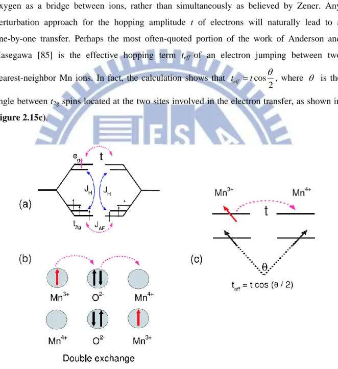
Figure 2.15: a) Schematic representation of the ideas of Zener to explain ferromagnetism. Zener envisioned a system with both localized and mobile electrons, which in the manganite language are the t2g and eg
electrons, as indicated. b) Schematic view of the DE mechanism. c) The effective hopping teff mechanism is drawn schematically [82] 31
Figure 2.16 Energy level diagram and 3d orbital eigenstates of Mn3+ in a crystal field
of cubic and tetragonal symmetry [82] 32
Figure 2.17 Low temperature resistance for a LCMO thin film with thickness of
t = 200 nm under different magnetic fields in-plane [88] 33
Figure 2.18 The spin polarization: a) Schematic density of states of a strong ferromagnet and b) half-metallic ferromagnet, re-drawn from Ref.[82] 35 Figure 2.19 a) The crystal structure and the Brillouin zone of YBCO; b) Tetragonal
structure of YBCO and c) Orthorhombic of YBCO [102] 38
Figure 2.20: a) – c): Phase diagram of YBa2Cu3Oy [102, 103]. AF: antiferromagnetic
insulator. SC: superconductor. d) Relationship between the oxygen
content y and the hole doping in YBCO [104] 39
Figure 2.21 Schematic diagram for the energies of Cu 3d and O 2p orbitals in the cuprates. In La2CuO4, for example, the Cu atom is surrounded by an
oxygen octahedron elongated along the z-direction [102] 41
Figure 2.22 Schematic pictures for the electron orbitals a), and b) the electronic structure c), d) of the CuO2 plane. Three bands, Cu 3dx2y2, O 2px and
2py, are considered in a) and c). Only the dx2y2 band at the Cu site is
Figure 2.23 In – plane resistivity as a function of temperatures with various doping
concentrations in YBCO [110, 111] 42
Chapter 3: Experimental Methods
Figure 3.1 a) The molecular beam expitaxy (MBE) laser deposition system used in this study. b) The schematic deposition process of MBE-PLD system 51 Figure 3.2 a) The typical scheme of double-axis diffractometer (left), and the corresponding motion for each angular motor in real space (right). (Figure courtesy of Panalytical B.V) b) The high-resolution triple-axis diffractometer (Huber 8 circle diffractometer) at NSRRC Beamline 17B1 (left), and the scheme of the corresponding motion of each angular motor
in real space (right) [15] 54
Figure 3.3 a) The detailed setup of a common TEM instrument. b) the concept of the image mode in TEM observation. c) The concept of the diffraction mode
in TEM observation [8] 56
Figure 3.4 a)The instrumental depiction for AFM operation. (copyright@nanodic.com) b) The correspondingly operative region of three typical modes of AFM in
Lennard-Jones pair potential energy [16] 57
Figure 3.5 a) Structural variations depend on the polarization sign in vertical PFM manipulations, which cause the deflection of laser signal in photodetector. (Figure courtesy of S. Jesse, ORNL.) b) Two types of distortion of cantilever in in-plane PFM manipulations: torsion and buckling. The torsion makes the laser signal a horizontal shift in photodiode, whereas
the buckling will make a similar feature to deflection [16] 60
Figure 3.6 Schematic representation of a Josephson device (or a simple SQUID magnetometer) interacted with a magnetic field. The change of magnetic flux will induce a variation in measured voltage. (Redrawn from the website http://hyperphysics.phy-astr.gsu.edu/hbase/solids/squid.html) 62 Figure 3.7 Principles of X-ray absorption spectroscopy, using a one-electron model a) Transmission mode and while b) is the total electron yield mode [17,18] 64 Figure 3.8 Principles of X-ray absorption spectroscopy, using a one-electron model
for Fluorescence mode [18] 65
Figure 3.9 Schematic diagram of x-ray magnetic circular dichroism (XMCD). a) Experimental set up for XMCD measurements. b) Circularly polarized
XI
x-ray absorption spectra. c) Transition probability of 2p → 3d absorption with circularly polarized x rays for less-than-half filled 3d electronic
configuration [21] 66
Figure 3.10 Principle of X- Ray photoelectron spectroscopy [21] 68
Figure 3.11Typical Van-der-Pauw geometry on a sample. Labels A to D indicated
current and voltage contact and was redrawn from Ref.[22] 71
Figure 3.12 Illustration of the substrate treatment processes to obtain the TiO2-
terminated on the surface of STO(100) substrate 72
Chapter 4: Ferroelectric control of the conduction at the LaAlO3/SrTiO3
hetero-interface
Figure 4.1 RHEED oscillations for the growth control the LAO thickness (illustration for 6uc of LAO) by Laser MBE system. The insets show the RHEED patter at the beginning (before) and end (after) of the LAO growth (lover panel in the left and right) and also AFM image scanning for LAO 6uc on
TiO2- STO substrate (higher panel) 75
Figure 4.2 The structural characterization; a) Grown and schematic model of the PZT/LAO/STO structure; b) XRD θ-2θ scans shows only the PZT (00L) peaks can be observed in the vicinity of STO peaks of the PZT/LAO/STO thin film; c) Off – normal Reciprocal space mapping (RSM) scan around the STO (103) peak. The LAO and PZT (103) peaks can be observed together with STO peak. The insert figure is the In -plane epitaxy revealed by Φ-scan of the thin film peaks are well aligned on our substrate; d) TEM investigation of the PZT20nm on top of LAO6uc/STO heterointerface, a high – resolution HAADF image showing an atomically sharp interface of both LAO and PZT films on TiO2 –terminated STO substrate. The dimension of the scale bar is
1nm; e) Mechanically induced reversal of the ferroelectric polarization. The piezoresponse force microscopy (PFM) techniques shows that only two contrasts can be observed in the mapping of the piezoresponse signal and single – point PFM hysteresis loops of the PZT film on LAO/STO
heterointerface in f) 78
Figure 4.3 Transport measurement of PZT/LAO/STO devices: a) Sketch of the samples and the contact configurations down to the LAO/STO interface by using the IB lithography method; b) Temperature dependence of the sheet resistance, Rs, of the PZT thickness dependence on n–type
LAO/STO conducting interface; c) Influence of LAO thickness on the electronic properties of the PZT/LAO/STO devices while keeping the constant at 20nm of PZT on top of LAO/STO hetero-interface. d) Sheet resistance measured as a function of temperature for PZT 20nm/LAO 3uc/STO as grown with natural polarization (Pup) and after switching the
polarization to down states (Pdown); e) Modulation of sheet resistance from
high to low resistance states of two samples, PZT(20 nm)/LAO(6 uc)/STO and PZT(20 nm)/LAO(4 uc)/STO corresponding to natural polarization (Pup) and after switching (Pdown), respectively 80
Figure 4.4 The sheet resistance as a function of temperature measured for the as –grown device with nature polarization (upward -Pup) (green),
Mechanically downward –switched the polarization (Pdown- blue color)
and reversal the polarization back to the original state (Pup- red color),
then sheet resistance becomes high state again 81
Figure 4.5 X-ray Photoemission spectroscopy study on the upward / downward ferroelectric polarization PZT/LAO/STO and LAO/STO hetero-structure. a) Schematic illustration of the photoemission spectroscopy measurement on the upward (Pup) / downward (Pdown) polarization of the
PZT/LAO/STO, and the bare LAO/STO samples also included in the Figure. The Pb 4f, La 4d and Sr 3d (indicated by green, yellow and blue arrow) are captured from PZT, LAO and STO layers separately (indicated by green, yellow and blue block). b) The XPS spectra taken from the PZT/LAO/STO and bare LAO/STO samples. The photoelectron peaks are aligned into the same energy level in the Pb4f and La4d (guided by red dashed line). But the Sr 3d core-level has significant binding energy downward shift from 0.15 to -0.1 eV when the Pup ferroelectric PZT
switched to Pdown (see inserted Figure) 83
Figure 4.6 a) A typical cross-sectional constant current STM image of the epitaxial PZT/LAO/STO hetero-structure. The spatial spectroscopic measurements on LAO surfaces of PZT/LAO/STO systems for the b) upward-polarized (Pup) and c) downward-polarized (Pdown) situation in PZT films from the
position near the STO side (N), the middle side of LAO (M), to the position away from STO (A). The average spatial spectroscopic measurements on LAO (green curve), and STO (orange curve) surfaces
XIII
for the d) upward-polarized (Pup) and e) downward-polarized (Pdown)
situation in PZT films 86
Figure 4.7 Ec band bending a), electron concentration and local electronic
conductivity b) in STO layer in the presence of upward polarization, no polarization and downward polarization in PZT layer (z denotes the position in the STO layer, H is half of the layer thick ness, so that z/H from -1 to +1 represents the entire layer). c) Schematic band diagrams of a PZT/LAO/STO heterointerface derived from ferroelectric-pattern assisted XPS and XSTM/S measurements. The sheet of negative/positive bound charges at bottom PZT an d its induced E-field (EPZT) across the LAO layer would directly affect
the mobile charges depletion/accumulation at the LAO/STO heterointerface, which are shown for both polarization states (Pup
and Pdown) of PZT layer. Decrease and increase potential bui ldups
across LAO layer corresponded to different polarization states are indicated. Combining both XPS and STS spectroscopic results, the changes in valence band offset (ΔEVBO) and core-level energetic
separation (ΔECL) between LAO and STO layers are revealed, and
construct a ferroelectricity modulated LAO/STO band structure
model 88
Chapter 5: Termination Control of Charge Transfer in YBa2Cu3O7-x/
La0.7Ca0.3MnO3 heterostructures
Figure 5.1 Inverse proximity effect: One electron of a Cooper pair which resides mainly in the ferromagnet aligns its spin parallel to the ferromagnetic moment. However, the second electron of the same Cooper pair which resides mainly in the superconductor aligns its spin antiparallel to conserve the Cooper pair’s singlet state. This figure was taken from [26] 98 Table 5.1 Physical parameters for representative SL’s and films grown by laser ablation
(taken from [39]) 102
Figure 5.2 Epitaxial design of heterointerfaces: Schematic of the interfacial control of LCMO/YBCOd with different interfaces; a) in the MnO2-terminated
interface (La0.7Ca0.3O–MnO2–BaO–CuO2) the charges are very difficult to
a dashed line) while b) switches into the La0.7Ca0.3O-terminated
(MnO2–La0.7Ca0.3O–CuO2–BaO) interface by using SRO; electrons
transfer easily from LCMO to YBCO because of the CuO chain at the
interface (indicated by solid lines) 104
Figure 5.3 Interface control “Growth model”: Layer–by –layer growth is monitored by RHEED, a) the MnO2-terminated interface corresponds to the
STO/LCMO10nm/YBCOd structure while b) the La0.7Ca0.3O-terminated
interface has the following STO/SRO1nm/LCMO10nm/YBCOd structure
105 Figure 5.4 (color online) Transport properties of LCMO/YBCOd with different
interfaces: Resistivity vs. temperature of LCMO/YBCOd a) d=6nm, b)
d=20nm, c) d=100nm, and d) Superconducting temperature, Tc, as a
function of YBCO thickness for both the MnO2- and
La0.7Ca0.3O-terminated interfaces 107
Figure 5.5 (color online) a) Temperature dependence of the field cooled magnetization measured in H = 100Oe out-of-plane; Inset shows the M-H loops of LCMO/YBCOd with different interfaces recorded at 100K and
with H applied out-of-plane along [100]STO directions. b) Low- temperature magnetization as a function of YBCO layer thickness for the two different interfaces. c) Mn L2,3 –edge spectra of the YBCO
(2nm)/LCMO (10nm) bilayer with different interfacial terminations taken with circularly polarized x-rays at T=30K. The photon spin was aligned parallel (μ+, green) or antiparallel (μ
-, orange) to the 1 T magnetic field. The field was applied along the surface normally; Mn-L2,3 XMCD signal
with the La0.7Ca0.3O-terminated interface (red line) and the
MnO2-terminated interface (black line) for LCMO/YBCOd are shown in
lower panel 110
Figure 5.6 (color online) a) Mn K -edge XAS spectra LCMO/YBCOd with different
interfaces at thickness of YBCO is d =10nm and plot together with the Mn2O3 (Mn3+) and MnO2 (Mn4+) standard samples spectra , taken in
fluorescence yield mode . b) Mn valence states vs absorption edge energy (eV) of the MnO2-terminated (black symbols) and La0.7Ca0.3O-terminated
(red symbols) samples; La1-xCaxMnO3 (where x =0, 0.3, 0.6, and 1) was used
XV
standard samples to determine the Mn valence state. c) Mn valence states as a function of YBCO thickness on the different interfaces 112 Figure 5.7 (color online) a) - c) O K -edge XAS spectra LCMO/YBCOd with different
interfaces vary thickness of YBCO is d =6nm, 13nm, and 50nm. d) Comparison of O K- edges XAS spectra LCMO/YBCOd with different
interfaces with YBCO thicknesses of 13nm, 20nm and 50nm, taken in
sample current mode 113
Figure 5.8 (color online) Comparison of O K- edges XAS spectra LCMO/YBCOd
with different interfaces with YBCO thicknesses of 13nm, 20nm and
50nm, taken in Fluorescence yield mode 114
Figure 5.9 The O K –edge XAS spectra illustrate the contribution of oxygen in different layers of structures: Enlarged peaks of oxygen in STO, LCMO and YBCO located at 531eV, 529.3eV and 527.8 eV, respectively 115 Figure 5.10 The procedure to normalize the O K –edge XAS spectra: a) The structures with two different interfaces of LCMO/YBCO indicating the thickness and number of oxygen in one unit cell of each layer, in subscript and parenthesis, respectively for sample current mode. b) and c) the spectra after normalization and showing that the contribution of oxygen in our samples is very clear and can be separated from LCMO and STO 116 Table 5.2 Total number of oxygen with different thicknesses of YBCO of two
different terminated interfaces 117
Figure 5.11 Mn K -edge XAS spectra for LCMO/YBCOd with different interfaces at
thickness of YBCO being 6nm, 10nm, 13nm, 20nm and are plotted together with spectra for the Mn2O3 (Mn3+) and MnO2 (Mn4+) standard
samples and reference samples , taken in fluorescence yield mode to
demonstrate how to determine the valence state of Mn 119
Figure 5.12 a)-c) Mn-L2,3 edge XAS spectra for LCMO/YBCOd with different
interfaces with YBCO thicknesses of 2nm, 6nm and 8nm; d) Comparison of Mn L- edges XAS spectra LCMO/YBCOd with different interfaces
with YBCO thicknesses of 2nm, 6nm and 8nm, and showing clearly the energy shifts after putting the YBCO thicker, taken in total electron yield
Appendix B. Electric field in LAO calculations
Figure B1. X-profile of PZT spontaneous polarization in the stripe 180-degree domain structure (a, b), stray depolarizing field E3(x,z) existing in LAO layer (c, d) and “sheet” charge S(x) located in the vicinity of STO surface (e,f). PZT thickness L=50 l.c., LAO thickness H1=4, H2=5, H3=6 l.c.,
depth z1=0, z2=0.5H, z3=H, domain structure period a=100 l.c. (a, c, e)
and a=10 l.c. (b,d, f). Abbreviation l.c. stands for lattice constant units.
Appendix C. Phase-Field Modeling of Ferroelectric Modulation at LAO/STO Interface
Figure C1. (a) Schematic band diagram of STO/LAO/PZT heterojunction; (b) the electric potential distribution in the absence of polarization; (c) the electron concentration in the absence of polarization (z denotes the position in the STO layer, H is half of the layer thickness, so that z/H from -1 to +1 represents the entire layer)
Figure C2. Schematic band diagrams of a PZT/LAO/STO heterojunction in the presence of upward polarization Pup (a) and downward polarization Pdown
(b) in PZT layer. The polarization bound charge and electric potential distribution in PZT layer with upward polarization (c) and (d), and with downward polarization (e) and (f)
Figure C3. Comparison of electric potential, electron concentration and local electronic conductivity in STO layer in the presence of upward polarization, no polarization and downward polarization in PZT layer (z denotes the position in the STO layer, H is half of the layer thickness, so that z/H from -1 to +1 represents the entire layer).
1
Chapter 1: Introduction
As we have known that heterointerfaces based on perovskite oxidies have heralded the possibility of creating new multifunctional properties which would not have been possible to be found by using single-phase bulk materials. The discovery of electronic reconstruction caused the conducting at oxide interfaces has attracted a lot of interest and attention. In addition, heterointerfaces based on oxide thin films show a broad spectrum of generating richer functionality than available with the present conventional semiconductors [1-3]. Since atomic-layer control of the growth is possible in the oxide heterostructures family, the planes along the c axis in the ABO3 perovskite structures can be grown by two alternating layers of
AO and BO2 planes at the interface. When interface effects dominate, different atomic layer
stacking sequence at the interfaces presents a variety of opportunities to couple different physical properties at these heterostructures in small length scales. Several studies have successfully demonstrated the unusual atomic and electronic structure at the solid-solid interface of heterostructures [3-7].
A particularly interesting example seems to be presence of a conducting quasi-two electron gas at the interface between the two insulators LaAlO3 (LAO) and SrTiO3 (STO),
depending on the terminating layer of the interface. Recently, Ohtomo and Hwang [7] found different electronic behaviour for thin LaAlO3 films on either SrO- or TiO2 -terminated
SrTiO3 substrates, the former interface being insulating and the later interface being n-type
conductor. Similar behaviour was found for the LaTiO3 – SrTiO3 interface [8]. So controlling
the terminations at the interfaces would be also a key point to study the oxide interfaces. Therefore I have decided to study “Controlling the interaction in complex oxide interfaces” as my doctoral thesis. In the push for practical applications, it is desirable to have the ability to modulate the interface functionalities by external stimulus. So, in the first part of my thesis, “Ferroelectric control of the conduction at the LAO/STO hetero-interface”, we propose a generic approach by inserting a functional layer to the heterostructure to acquire the non-volatile control of the intriguing properties at oxide interfaces. The LAO/STO interface is served as a model system in which a highly mobile quasi-two dimensional electron gas (2DEG) forms between two band insulators [7, 9], exhibiting 2D superconductivity [10] and unusual magnetotransport properties [11]. In this study, we bring in a ferroelectric Pb(Zr0.2Ti0.8)O3(PZT) layer nearby the LAO/STO interface. The ferroelectric polarization of
PZT layer serves as a control parameter to modulate the 2DEG conducting behaviors. The as-grown polarization leads to charge depletion and consequently a low conduction.
Switching the polarization direction results in a charge accumulation and enhances the conduction at the interface of LAO/STO.
The second part of my thesis, with the title “Termination control of the charge transfer in YBCO/LCMO hetero-structures” is presented in chapter 5. In this part, we study coupling between ferromagnetic (F) and superconductors (S) with two distinct interfaces. It would be one of the topical interests because they offer the appropriate scenario to study competing effects of superconductivity and ferromagnetism on the scale of their characteristics lengths. In addition, coupling between F and S may be understood in two different scenarios: firstly, Cooper pairs of the superconductor may enter the ferromagnet (proximity effect). Second, spins of ferromagnet may enter the superconductor, therefore the proximity effects in F/S interfaces are related to new physical phenomena arising from the interaction between two order parameters that may find potential applications in development of superconductivity and magnetoresistance memory devices. Recent studies the advanced synthesis of epitaxial heterostructures of transition metal oxides, offer intriguing perspectives for the practical realization of such oxide hetero-interfaces. In this regard, Ferromagnetic LCMO and high - temperature superconductor YBCO have been investigated with a variety of experimental methods [2, 12, 13, 14, 15]. However, we are the first ones to examine the coupling between ferromagnetism and superconductivity in La2/3Ca1/3MnO3 / YBa2Cu3O7-x heterostructure with
different interfaces by Epitaxial design of heterointerfaces. Since both YBCO and LCMO have the ABO3 perovskite structure, two possible atomic stacking sequences can be formed in
(001) – oriented heterostuctures, La0.7Ca0.3O –MnO2 – BaO – CuO2 (MnO2 – terminated
interface) and MnO2 –La0.7Ca0.3O – CuO2 – BaO (La0.7Ca0.3O – terminated interface). In order
to realize this interfacial design, atomically precise interface control is needed and can be achieved by designing LCMO layers with well defined atomic terminations using RHEED controlled PLD growth clearly showing the intensity of oscillation of the specular reflection spot, that indicates a layer –by – layer growth mode with one unit cell precision.
The main focus of this thesis is, controlling the conduction of 2DEG at LAO/STO interface using the ferroelectricity of PZT and study of coupling between the ferromagnetism and superconducting in YBCO/LCMO with different interfaces to understand the physics and explore their applicability in new devices. Therefore, outline of my thesis will include the following parts.
Chapter 2 and chapter 3 of my thesis will give basic background to the rest of this booklet. Chapter two provides an overview of correlated-electron physics, 2DEG and background to the materials such as PZT, LCMO and YBCO, covering basic ideas as well as
3
a literature review of relevant work. Chapter three discusses the various techniques to fabricate and analyze these structures. This also covers sample preparation and fabrication, as well as in situ and ex situ analysis methods.
The two most important chapters of the thesis, chapter 4 and 5, collate data from some of the experiments during my Ph.D. research. The growth of PZT/LAO/STO and LCMO/YBCO with different interfaces and he properties of these structures as a function of growth parameters such as the functional thickness of each layer during deposition, deposition duration or heterostructure design are discussed. To be more precise, chapter four discusses the structural characterization, electrical transport, X-ray spectroscopy (XPS) and Cross –sectional scanning tunneling microscopy in detail and spectroscopy measurements provide collaborating results. Besides, the theoretical calculations and discussions are also presented. Chapter 5 focuses on the “termination control of the charge transfer in LCMO/YBCO heterostructures. The principles of experiments are similar to those in chapter four, however, here we focus more on how to fabricate with two distinct interfaces to study the coupling between the ferromagnetism and superconducting. Then we also provide the results of the transport measurements and magnetic properties to show quantitatively, how the interface control can manipulate the physical properties in both YBCO and LCMO functional layers. Moreover, the results from XAS provide evidences for the charge transfer at different interfaces which illustrate that only atomically precise control of this interface enabled us to identify a new mechanism of charge transfer in the YBa2Cu3O7-x/La0.7Ca0.3MnO3
hetrostructures.
Finally, my thesis closes with a brief summary and supporting materials based on theoretical calculations for the experimental results presented in chapter 5.
References
[1] A. Gozar, G. Logvenov, L. Fitting Kourkoutis, A. T. Bollinger, L. A. Giannuzzi, D. A. Muller, I. Bozovic, Nature 2008, 455, 782.
[2] J. Chakhalian, J. W. Freeland, G. Srajer, J. Strempfer, G. Khaliullin, J. C. Cezar, T. Charlton, R. Dalgliesh, C. Bernhard, G. Cristiani, H.-U. Habermeier, B. Keimer, Nat. Phys.
2006, 2, 244.
[3] A. Ohtomo, D. A. Muller, J. L. Grazul, H. Y. Hwang, Nature 2002, 419, 378.
[4] W. A. Harrison, E. A. Kraut, J. R. Waldrop, R. W. Grant, Phys. Rev. B 1978, 18, 4402. [5] G. A. Baraff, J.A. Appelbaum, D. R. Hamann, Phys. Rev. Lett. 1977, 38, 237-40. [6] Y. Hotta, T. Susaki, H. Y. Hwang, Phys. Rev. Lett. 2007, 99, 236805.
[7] A. Ohtomo, H. Y. Hwang, Nature 2004, 427, 423–426.
[8] S. Okamoto, A. J. Millis, and N. A. Spaldin, Phys. Rev. Lett. 2006, 97, 056802. [9] N. Nakagawa, H. Y. Hwang, D. A. Muller, Nature Mater. 2006, 5, 204–209
[10] N. Reyren, S. Thiel, A. D. Caviglia, L. F. Kourkoutis, G. Hammerl, C. Richter, C. W. Schneider, T. Koop, A. -S. Rüetschi, D. Jaccard, M. Gabay, D.A. Muller, J. -M. Triscone, J. Mannhart, Science 2007, 317, 1196–1199.
[11] A. Brinkman, M. Huijben, M. van Zalk, J. Huijben, U. Zeitler, J. C. Maan, W. G. van der Wiel, G. Rijnders, D. H. A. Blank, H. Hilgenkamp, Nature Mater. 2007, 6, 493–496. [12] Chakhalian, J.; Freeland, J.W.; Habermeier, H,-U.; Cristiani, G.; Khaliullin, G.; van Veenendaal, M.; Keimer, B. Science. 2007, 318, 1114–1117.
[13] Stahn, J.; Chakhalian, J.; Niedermayer, Ch.; Hoppler, J.; Gutberlet, T.; Voigt, J.; Treubel, F.; Habermeier, H.-U.; Cristiani, G.; Keimer, B.; Bernhard, C. Phys. Rev. B. 2005, 71, 140509.
[14] Soltan, S.; Albrecht, J.; Habermeier, H.-U. Phys. Rev. B. 2004, 70, 144517.
[15] Sefrioui, Z.; Arias, D.; Pena, V.; Villeegas, J.E.; Varela, M.; Prieto, P.; Leon, C.; Martinez, J.L.; Santamaria, J. Phys. Rev. B. 2003, 67, 214511.
5
Chapter 2: Background
Recently, heterointerfaces between the complex oxides materials have been an interesting class encompassing the full spepiezoelectric in electronic field, ferromagnetic, multiferroic in magnetic field of physical properties, such as insulating, semiconducting, metallic, superconducting, ferroelectric, and ear optical effects in optics field. These vast physical properties also have a strong correlation to structural variation that can be induced by ambient condition like temperature, pressure, magnetic field, electric field, etc., and offer new opportunities for electronic applications. This chapter will give an basic introduction to the key concepts of two dimensional electron gas (2DEG) LAO/STO interface, ferroelectricity of PZT, ferromagnetism of LCMO and superconducting of YBCO and describe the detailed information of corresponding materials in this work.
2.1. Some concepts about 2DEG in correlated-electron oxides and semiconductors 2.1.1 Introduction
One of the fastest and most pervasive technologies of the last decades was semiconductor physics. In a fascinating interplay between theoretical understanding, experimental acumen and technological applications the field was developed rapidly and extensively due to fascinating physical properties and also offering more possibilities for the next generation of electronic devices. Therefore, most of studies are arming at exploring the new interfaces to create the new functionalities. Moreover, in strongly correlated oxide interfaces, heterointerfaces provide a powerful round to manipulate the physical properties (charge, spin, orbital and lattice degree of freedom) and also understand the physics behind which are not able to be found in the single bulk materials. Moore's law [1] would not have been possible without this development. Two-dimensional electron gases (2DEG) probably are one of the prime examples of this innovation. It can be understood the fundamental and principles of 2DEG from quantum mechanics (it can be found in any quantum mechanics books like Sakurai [2] or David Grifiths [3]), and their realization was only made possible once the experimental fabrication techniques were well developed ; there was a gap of about 50 years between concept and device. Once available though, the 2DEG provided a path way and new opportunities for research and development to our future devices. Now we can strongly confirm that 2DEG of LAO/STO is device. In recent years the growth of transition
metal oxides have been studied by different methods, especially by Pulsed laser deposition (PLD) or laser Molecular beam epitaxial (MBE), and has risen to similar levels of control and
in situ monitoring [4, 5] resulting in the fabrication of high-quality films and heterostructures
of these oxides [6–9 ]. This small part of the chapter gives an overview of theory of quantum wells and correlated electron materials as well as previous work on the systems under investigation here: LAO/STO interfaces. This lays the physics foundation in the later chapters.
2.1.2 The physics background of 2DEG
In Quantum Mechanics, the based and also the fundamental problem is considered the particle-in-a-box example in which a single particle is confined to a certain area by an external potential and described by the time – independent Schrodinger's equation as follows (one-dimensional): 2 2 2 2 d V E m dx (2.1)
where (ħ) is the reduced Planck's constant, m is the mass of particle, is the total wave function of electrons, x is the position, V is the (in) finite external potential and E the (eigen) energy of the system. For an in finite external potential, the particle is truly confined, in this case the energies are quantized as
2 2 2 8 n n h E mL (2.2)
where n is the quantum number and L is the size of the potential well. Or if we set k=n/2L and as the wave number and h= ħ/2, we obtained:
2 2 2 n k E m (2.3)
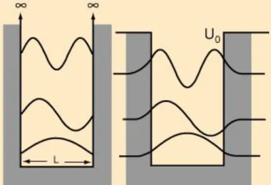
For the realistic case, the potential is finite and the wave function is not completely contained within the potential well. This is shown schematically in Figure 2.1. This simple one-dimensional picture can be extended to three dimensions, but in my thesis, we just focus on two-dimensional layers which electrons are confined in only one direction in between the interface of LAO and STO layers of n-type interface. In such of that the particles are confined perpendicular to the layer, but are free to move within the layer (in plane). In that case, any additional quantum properties are well described by the one-dimensional case.
7
Figure 2.1 The energy levels of electrons in quantum well: an infinite (left) and a finite
(right), taken from Ref. [10].
2.1.2.1 Potential wells in semiconductors
So far quantum theory has shown that a single particle in a potential well has distinct, numbered energy levels. To realize such a 2DEG system in an experimental device, three conditions need to be met:
1. There has to be a potential well;
2. There have to be particles, here electrons, within the potential well; 3. The electrons within the well should not interact significantly.
Figure 2.2 The band structures of simple single materials: a) insulators, b) semiconductors
Again, the interplay between theory and experiments should be the pathway to such future devices. The application of quantum mechanics to solid state science gave rise to band structure theory. There, the (electrical) properties of materials are defined by the appearance of collections of electron levels named bands which we would like to introduce in Figure 2.2.
If the Fermi level is within a gap between two bands and thermal fluctuations do not excite some electrons to the upper, conducting band, the material is an insulator (see Figure
2.2a)). However, if some electrons are excited to the conduction band, it is a semiconductor
(Figure 2.2b)). If the Fermi level, the maximum energy level electrons can reach if the system is in its ground state, is within such a band, it is a conductor. See Figure 2.2 c). The band gap is unique for each semiconductor material. Table 2.1 shows some band gaps for representative semiconductors and oxides.
material band gap
Eg (eV) effective mass m* (–) electron mobility (cm2/Vs) electron density n (cm–3) Si 1.12 1.08 1300 2.0 .1016 GaAs 1.42 0.067 6000 3.0 .1015 AlAs 2.168 0.146 200 2.0 .1017 Nb:SrTiO3 1.8 6 3.2 1.4 .1017 LaAlO3 5.6 - - -
Table 2.1 Basic parameters for some representative semiconductors and oxides at room
temperature [12–16].
From Table 2.1 it can be seen that the band gap varies substantially. By layering different semiconductors a potential well can be created. An example of such a potential well is shown in Figure 2.3.
9
Figure 2.3 Band diagram of a simple semiconductor potential well, taken from Ref [16].
The problem is how to get electrons into the potential well. By doping in the semiconductor with atoms of an element that having valence electrons is also one of standard methods. Silicium is four-valent. Doping with phosphorus, which is five-valent would result in an excess of electrons after covalent bonding. These 'excess' electrons are now doped into the conduction band and can freely move throughout the potential well. Such doped atoms, however, also form scattering centers which inhibit mobility of the electron. As the electrons should be disturbed as little as possible within the potential well, the active layer (the central GaAs layer in Figure 2.3) should not be doped. Here an additional bonus of the potential well appears. If the layers to the side of the actual well are doped, the free electrons will search out the energy minimum within the well as their ground states. Therefore, the number of electrons within the well can be controlled, without disturbing the crystal perfection of the well itself. This control also gives the opportunity to make sure the electrons are independent from one another. As long as the mean free path is much smaller than the average distance between electrons and the electron-electron interaction will be negligible. Thus, by controlling the density of electrons within the potential well the independent electron regime can be maintained.
2.1.2.2 Independent vs. correlated electrons
With the time - independent electron approximation and the inclusion of electron correlation, the Schrodinger equation can be examined as the following form:
2 2 2 2 , , 1 2 i 2 i i j i j i j i j e e E m K r r K r R
(2.4)Where, the first term is free electron contribution. The other terms described the interactions formed by the other electrons and ions in the system. The second term of the Schrodinger equation describes the electron-electron interaction, while the third describes the electron-ion interaction. In the independent electron approximation the electron correlation is thought to be ignored. Also, the ions are much more massive than the electrons, so their movement is also negligible. These two assumptions greatly simplify Equation 2.4 and thus successfully lead to much of the solid state theory in the beginning of the last century. It made the complex Schrodinger equations tractable before the advance of complex numerical calculations like density functional theory that are nowadays able to work with the full, correlated Schrodinger equations. However, the independent electron approximation is not able to explain several important physical properties such as (anti)ferromagnetism, the Mott insulating state and superconductivity. The single-band Hubbard model is often used as a starting point of the discussion of correlated materials. It simplifies the treatment of the background ions, but explicitly includes the electron-electron interaction. The Hamiltonian of the model is given as:
† , ij i j i i i j i H t c c U n n
(2.5)where tij is the hopping parameter between nearest-neighbor sites i and j,ci(ci)
is the creation (annihilation) operator for an electron on site i with spin
or
, U is the Coulumb energy and ni c ci i is the electron occupation of site i. The physics of transfer integral captures where delocalizing an electron lowers its energy, similar to Bloch waves and thus represents the kinetic term from Equation 2.4. The Coulomb energy denotes the energy it costs to bring two electrons in close proximity, i.e. on the same site. By varying the total number of electrons and the relative energies of tij and U, a large phase space of properties opens upon. It is the recent and current interest in these properties then using the ferroelectricity to modulate the conductivity and their physical properties.11
2.1.3 Polar/non-polar interfaces
As we mentioned above, an example of a polar interface was described: the LAO (001) surface. There is a charge discontinuity between the LaO//AlO2 stacking and the 'vacuum'. The LAO consists in this orientation of alternating layer of (La O3 2 ) and (Al O3 22 ) while the vacuum has an effective charge of zero. Such discontinuities are often resolved by a surface reconstruction in bulk materials [17, 18]. However, such polar discontinuities can also occur inside heterointerfaces; a fact that is very famous from semiconductor physics, where it results in an ionic reconstruction at the interface between different semiconductors or in between layers of the materials have different band structures [19]. In correlated-electron materials, similar the redistribution of electrons to be found in the LTO/STO system. Moreover, the electronic reconstruction at domain walls in BiFeO3 is also found [20, 21, 22],
where the polarization discontinuity induced or enhanced to a conducting interface and the destruction of half–metal in Fe3O4/BaTiO3 due to the electron transfer across the interface
[23].
2.1.3.1 Charge transfer at LaAlO3/SrTiO3 interfaces
The big discovery in 2004, by Ohtomo and Hwang showed that the interface between LAO and STO in the (001) direction can be conducting, depending on the termination at the heterointerface. Such an interface exhibits a polar discontinuity, as LAO has alternating planes 1, while theSr O2 2and (Ti O4 22) planes of STO are neutral [24]. In a purely ionic picture, this discontinuity transfers either only half an electron per unit cell area from LAO into STO for a n-type interface or half a hole per unit cell area for an p-type interface.
Figure 2.4 shows how the electrons and holes are distributed in this model. The former
interface is found to be conducting as shown in Figure 2.4a) with TiO2 termination took a
place the top of STO (100) substrate, and we know it as n-type LAO/STO interface, while the latter, though nominally hole-doped, is insulating with SrO termination as Figure 2.4b) and is called as a p-type interface. Therefore, we can conclude that the hole-doping of closed shell ions is very difficult and complicated, moreover the compensation of holes by oxygen-vacancy would be a key point to be induced electrons results in no net free carriers [25, 26].
a) n-type interface b) p –type interface
Figure 2.4 The model of charge transfer at LAO/STO interfaces. Diagrams taken from
Ref.[25].
To understand the mechanism behind that, the purely ionic picture is never complete for a correlated-electron material. In other hand, more physical way to explain clearly these results is by looking at the internal dipole that develops across the charged in the LAO layers. In the electronically unreconstructed case, the transition of neutral to immediately charged layers results in a potential build-up due to the electric fields between the oppositely charged layers in LAO (see Figure 2.5). This 'polar catastrophe' grows with the LAO thickness and has to be compensated when the energy can no longer be accommodated by internal deformations [27–29]. In a band diagram, this happens when the potential build-up becomes larger in energy than the band gap of STO [29–32]. The valence band of LAO goes higher than the Fermi level, allowing for the charges transfer from the top surface to the interface. This reduces the potential build-up, as seen on the right panel in Figure 2.5. Recently, an argument has been made for the existence of in-gap states to which electrons can tunnel [33]. However, their theoretical calculations prove a constant electron density does not depend on the LAO layer thickness, contrary to experimental results [34, 35].
13
Figure 2.5 Illustration of the polar catastrophe in an unreconstructed case (left) and a
re-constructed case (right), where only half an electron is transferred into the TiO2 layer.
Diagrams are taken from Ref.[25].
To examine the n-type LAO/STO interface where the terminations at interface controlled by TiO2-LaO, the crossing of the potential build-up and the band gap implies that up to a
critical thickness of the LAO layer, this dipole can be accommodated by the strain within the LAO and no electronic reconstruction (i.e. electron-doping into the TiO2 layer) occurs. That
critical thickness has been found to be 4uc, below that it was still insulating, however, when the LAO thickness reaches 4uc, an abrupt change into conductivity interface [36]. Thicker LAO layers show a decreasing mobility, though the mechanism behind that behavior is one of the many unsolved mysteries in this system [35]. Theoretical calculations actually show a larger critical thickness, but this can have several explanations. One is that the supercell used in the calculations is too small, so we did not include all possible reconstructions of electrons [28, 37]. Another explanation is that in real samples there are surface defects that form in-gap states, so the LAO band needs to shift less before electrons are doped [29, 38]. Finally, (Density functional theory) DFT always has a problem calculating the band structure of materials, which may make these calculations only qualitative, not quantitative. This thickness effect can be used to pattern structures into the conducting layer by selectively depositing thick LAO [39]. Only in those areas where the LAO layer is thicker than 4uc the built in potential is large enough to trigger the electronic reconstruction at the interface and create a conducting interface. Or, by having the dipole develop to just below the threshold value for electronic reconstruction, the conducting state can then be induced by introduction to the LAO layer an electric field and thus altering the dipole across this layer. This can be
done either by a back-gate field-effect transistor configuration [36, 40] or by writing with a conducting AFM tip [41, 42]. Interestingly, this minimum thickness of LAO required for a conducting interface does not seem to apply when the LAO layer itself is again capped with STO. The created two different interfaces of LAO/STO (one is n-type, another is p-type) where n-type LAO/STO is conducting down to a single monolayer (unit cell) of LAO embedded in STO [34, 43, 44]. There is, however, a clear interaction between the two interfaces. Below a LAO thickness of about 6 uc the sheet resistance increases. Hall measurements show that this is due to a decrease of the electron density in the 2DEG, while the electron mobility is constant (as opposed to single interfaces, where the mobility decreasing with increasing thickness [35]). More interestingly, about half a year earlier a jump in the optical absorption spectrum of LAO/STO superlattices samples as observed which does not appear in alloyed films of the same chemical composition [45]. The LaNiO3/SrMnO3
system also undergoes an insulator-to-metal transition upon increasing the thickness of LaNiO3 layer [46]. Ionically, the system does have a polarization discontinuity (
3 3 2 4
3/ 3
La Ni O Sr Mn O ) so electron reconstruction may play a role here. The analysis of the transport behaviour points to a more complex conduction mechanism for this system compared to the LAO/STO system.
In general case, the electron gas acts as a Fermi liquid with a 1/ T behaviour of the 2 electron mobility[24, 34, 47–49], varying from ~ 6 cm2/Vs at room temperature to ~1000 cm2/Vs at 5 K. This correlated electron liquid model was confirmed by scanning tunneling spectroscopy [50]. Though in general the electron-electron interactions are weaker than electron-phonon interactions at room temperature, in STO they are typically weak (as seen from the poor heat conduction) and would give rise to different temperature dependence [34]. The electron density depends on so much of fabrication parameters such as substrate termination [47], oxygen pressure during deposition [24, 49, 51, 52] and, laser frequency in PLD chamber [53]. There is some argument for intermixing [25, 54, 55], but transmission electron microscopy images do not give conclusive evidence. Also, if intermixing would occur, the complimentary p-type interface should also become conducting [47]. A thermally-activated behavior of the electron density, similar to that in semiconductors, with an activated energy of about 6 meV was observed [34]. This point is weakly-bound donors as the source of the electrons [42]. In general, electron densities on the order of 10 cm14 2 at room temperature are achieved.
15
Remarkably, at low temperatures almost all data converge to a value around
13 2
2 10 cm [34, 36, 52, 56–58]. These values for the electron density would translate to, respectively, about 0.15 and 0.03 electron per unit cell area at room temperature and 5 K. This value is far below the nominal half electron per unit cell area transferred in the purely ionic model above. One explanation might be that the electrons are distributed over different sub-bands, of which only some contribute to the (Hall) free electron density [59]. However, XPS detects both free and bound electrons and the densities observed with this technique are close to those obtained from Hall measurements [60]. Table 2.2 compares the transport properties of semiconductor (Si and GaAs) and correlated-electron (LTO/STO and LAO/STO) systems. The electron mobilities in semiconductors are always higher than those in correlated-electron materials. This is not surprising, because the mobility is limited by the scattering of electrons, either from ions or with other electrons. Thus correlated-electron materials, with their higher electron densities, will almost always display lower mobilities than semiconductors. system m* (–) (cm2/Vs) n3D (cm–3 ) n2D (cm–2 ) Si 1.08 1300 2.0 .1016 GaAs 0.067 6000 3.0 .1015 ZnO / MgxZn1 – x O 0.32 160 2.5 .1013 Nb:STO 1.8 6 1.4 .1017 LTO / STO 1.8 3 8 .1021 LAO / / STO 1.5 6 1.2 .1014
Table 2.2 Comparison of the transport properties at room temperature for semiconductor
and correlated-electron systems, [12–14, 34, 61].
To study the possibility of quantum effects in these electron gases, the requirements for Shubnikov-de Haas oscillations can be studied. The occurrence of these oscillations is a clear sign of the quantum nature of the electron gas (see Table 2.2 and discussion).
2.2 Fundamental properties of Ferroelectricity (PZT)
A ferroelectric material is a subset of piezoelectrics which exhibits a spontaneous electric-polarization that can be reversed by the application of an external electric field.
2.2.1 Perovskite crystal structure
PZT crystallizes in perovskite structure. The illustration of crystal structure is shown in
Figure 2.6. Here we have used the ABO3 perovskite structure of Barium titanate (BaTiO3) as
an example. The corners sharing A site are occupied by Ba2+ ions; O2- ions occupy the interstices, which share electrons with neighboring cells; and Ti4+ ions occupy the central position, i.e B-site. In this figure, the central ion is not displaced, thus there is no dipole direction in the cubic phase being exhibited in the structure.
When the temperature is below the Curie temperature, a phase transition from the paraelectric phase to the ferroelectric one takes place in the crystal and electric dipoles form as the central ions displace with respect to the Ba2+ ions. In the tetragonal structure, there are 6 possible dipole directions which are corresponding to the central ion may shift up, down, left, right or in and out of the page. However, for the rhombohedral phase, the central ion is took a place along the diagonal towards any of the corner ions, resulting in 8 possible dipole directions. Therefore, one the central ions are displaced, that results in deformation of the shape of the entire cell. For example, when a tetragonal structure is formed as a result of the displacement of central ion in upward direction, the resulting unit cell elongates toward up-down directions. As a consequence, dipoles in neighbouring unit cells are displaced in the same direction, resulting in a knock on effect forming a region that is similar with dipole orientations, knowing as a domain in PZT or perovskite structure [62].
17
Figure 2.6 ABO3 perovskite crystal structure
2.2.2 Poling
Usually, polarization states of materials form as the natural polarization state of the as grown samples which depends on the materials, its natural polarization may have upward polarization state, downward polarization sate or even mixed states, and it can be switchable, so in order to produce a material with a net polarization and hence piezoelectric properties, domains need to be aligned. The switching polarization directions can be achieved by the application of an external electric field, resulting in the domains aligning with the field. Finally, when the electric field and heat are steadily removed and resulting the polarizations of the domains become ‘frozen’ in the new aligned directions. This process is called as ‘poling’ or “switching”. The polarization of a material after the poling field is removed is called the remnant polarization, PR. The maximum polarization achievable during poling is
restricted by the available domain states in the material, and it is a function of spontaneous polarization, Ps. In tetragonal polycrystalline ferroelectrics with 6 domain states, the maximum PR can be achieved is about 0.83PS. Whereas, comparing with the Rs, in a
rhombohedral polycrystalline ferroelectric with 8 domain states, the maximum PR achievable
is 0.87 Ps [63]. In practice, the achievable remnant polarization is always lower due to complex domain boundary and stress states.
![Table 2.1 Basic parameters for some representative semiconductors and oxides at room temperature [12–16]](https://thumb-ap.123doks.com/thumbv2/9libinfo/8720301.200469/26.892.126.813.303.848/table-basic-parameters-representative-semiconductors-oxides-room-temperature.webp)
![Figure 2.3 Band diagram of a simple semiconductor potential well, taken from Ref [16]](https://thumb-ap.123doks.com/thumbv2/9libinfo/8720301.200469/27.892.135.807.127.898/figure-band-diagram-simple-semiconductor-potential-taken-ref.webp)
![Figure 2.4 The model of charge transfer at LAO/STO interfaces. Diagrams taken from Ref.[25]](https://thumb-ap.123doks.com/thumbv2/9libinfo/8720301.200469/30.892.130.813.129.858/figure-model-charge-transfer-lao-interfaces-diagrams-taken.webp)
![Table 2.2 Comparison of the transport properties at room temperature for semiconductor and correlated-electron systems, [12–14, 34, 61]](https://thumb-ap.123doks.com/thumbv2/9libinfo/8720301.200469/33.892.135.817.437.872/comparison-transport-properties-temperature-semiconductor-correlated-electron-systems.webp)
![Figure 2.7 Hysteresis loop of a ferroelectric material: ferroelectric polarization as a function of the applied electric field [62]](https://thumb-ap.123doks.com/thumbv2/9libinfo/8720301.200469/36.892.130.810.255.1034/figure-hysteresis-ferroelectric-material-ferroelectric-polarization-function-electric.webp)
![Figure 2.11 Schematic illustration of five basic types of magnetic orders [69].](https://thumb-ap.123doks.com/thumbv2/9libinfo/8720301.200469/41.892.138.803.103.767/figure-schematic-illustration-basic-types-magnetic-orders.webp)
![Figure 2.14: The phase diagram of La 1-x Ca x MnO 3 , after Cheong and Hwang [81]. There exist well-defind anomalies at](https://thumb-ap.123doks.com/thumbv2/9libinfo/8720301.200469/47.892.128.802.218.899/figure-phase-diagram-cheong-hwang-exist-defind-anomalies.webp)
![Figure 2.16 Energy level diagram and 3d orbital eigenstates of Mn 3+ in a crystal field of cubic and tetragonal symmetry [82]](https://thumb-ap.123doks.com/thumbv2/9libinfo/8720301.200469/50.892.127.814.394.1038/figure-energy-diagram-orbital-eigenstates-crystal-tetragonal-symmetry.webp)
