國 立 交 通 大 學
光電工程研究所
碩士論文
非晶矽矽鍺合金作為薄膜太陽能電池吸收層:
特性、最佳化以及元件特性之研究
a-Si
1-x
Ge
x
:H Alloy as Absorber Layer for Thin
Film Solar Cell :
Characterization, Optimization, and Device
Performance
研究生:王建敏
指導教授:蔡娟娟 教授
非晶矽矽鍺合金作為薄膜太陽能電池吸收層
非晶矽矽鍺合金作為薄膜太陽能電池吸收層
非晶矽矽鍺合金作為薄膜太陽能電池吸收層
非晶矽矽鍺合金作為薄膜太陽能電池吸收層:
::
:
特性
特性
特性
特性、
、
、最佳化以及元件特性之研
、
最佳化以及元件特性之研
最佳化以及元件特性之研
最佳化以及元件特性之研究
究
究
究
a-Si
1-xGe
x:H Alloy as Absorber Layer for Thin Film Solar Cell :
Characterization, Optimization, and Device Performance
研究生:王建敏 Master Student : Chien-Ming Wang
指導教授:蔡娟娟 教授 Advisor : Prof. C.C. Tsai
國 立 交 通 大 學
光電工程研究所
碩士論文
A thesis
Submitted to Department of Photonics
College of Electrical Engineering and Computer Science National Chiao Tung University
In partial Fulfillment of the Requirements For the Degree of
Master In
Electro-Optical Engineering August 2009
Hsinchu, Taiwan, Republic of China 中華民國九十八年八月
非晶矽
非晶矽
非晶矽
非晶矽矽
矽
矽鍺合金作為薄膜太陽能電池吸收層
矽
鍺合金作為薄膜太陽能電池吸收層
鍺合金作為薄膜太陽能電池吸收層
鍺合金作為薄膜太陽能電池吸收層:
::
:
特性
特性
特性
特性、
、
、
、最佳化以及元件特性之研究
最佳化以及元件特性之研究
最佳化以及元件特性之研究
最佳化以及元件特性之研究
研究生
研究生
研究生
研究生:
::
:王建敏
王建敏
王建敏
王建敏
指導教授
指導教授:
指導教授
指導教授
::
:蔡娟娟
蔡娟娟
蔡娟娟
蔡娟娟
教授
教授
教授
教授
國立
國立
國立
國立交通大學
交通大學
交通大學
交通大學光電工程研究所
光電工程研究所
光電工程研究所
光電工程研究所
摘要
摘要
摘要
摘要
在本研究中,藉著改變氫流率、電漿功率、以及製程氣體和電極間距來研究非晶矽 鍺薄膜特性以及太陽能發光效率。 製程氣體我們使用矽甲烷(SiH4)、鍺甲烷(GeH4)以及 氫氣,利用 射頻電漿輔助化學氣相沉積系統(PECVD)來沉積非晶矽鍺薄膜。由本篇實驗 發現通入適當氫氣可提升光電導,而鍺原子濃度亦影響光學能隙以及電性。電漿功率除 了會影響薄膜沉積速率外同時亦可提升電性。在元件的表現來說,較高的 Xg (Xg= GeH4 / (GeH4+SiH4)) 值讓的元件短路電流下降並造成太陽能電池的發光效率由 6.33% 降低至 4.85 %。
a-Si1-xGex:H Alloy as Absorber Layer for Thin Film Solar Cell :
Characterization, Optimization, and Device Performance
Master Student: Chien-Min Wang Advisor: Dr. Chuang-Chuang Tsai
Dept. of Photonics and Inst. of Electro-Optical Engineering & Display Inst.,
National Chiao Tung University
Abstract
In this study, the effects of systematic variation in hydrogen dilution, RF power, gas phase ratio of germane (Xg), the electrode spacings (E/S) on the amorphous silicon
germanium alloy (a-Si1-xGex:H) properties and single junction solar cell performance have
been studied. The hydrogenated amorphous silicon germanium films were deposited from the mixture of SiH4,GeH4 , and H2 dilution by the plasma enhanced chemical vapor deposition
(PECVD) system at 27.12 MHz. It has been found that hydrogen dilution plays an important role in the properties of films. Adequate hydrogen dilution ratio can improve the photo conductivity and photosensitivity, but the higher or lower hydrogen dilution ratio both deteriorates the film properties. Power density influences on the deposition rate and electronic properties. Photo conductivity is higher for films deposited at higher power density for all hydrogen dilution ratios. Dark conductivity is almost the same for films
deposited at two different power densities for all hydrogen dilution ratios. Germane to silane ratio (Xg) plays a leading role in single junction solar cell performance. Increasing gas phase
ratio of germane (Xg) can raise the short circuit current (Jsc), but the higher Xg value will
reduce the fill factor (F.F.) from 60.6 % to 48.71 % and deteriorate the cell efficiency from 6.326 % to 4.85 %. From the result of the quantum efficiency spectra, the spectral sensitivity of solar cell extends systematically towards longer wavelengths as increasing the Xg value in i layer from 8.3% to 16.7 %. To compare the amorphous silicon solar cell, when
誌謝
誌謝
誌謝
誌謝
誌謝是這本論文最後完成的部分,在書寫誌謝的當下,兩年來的記憶不斷在腦海裡 撥放著,這些日子來的研究生活的確是點滴在心頭。經過了兩年碩士的洗禮,讓我想起 聖經裡的一句話。聖經說:上帝要大大傾福於你,必要使你無處可容。 首先我要先感謝我的指導老師蔡娟娟老師,老師對產業未來趨勢的判斷和國際觀令 我大開眼界;老師也時常邀請國際級大師蒞臨交大演說,這同時讓我見識到了國際級的 研究水準以及英文的重要性。也由於我們是第一屆學生,老師也給與我們相當多在研究 領域外的學習機會,例如機台設備的引進組裝規畫,也有許多機會能跟廠商人員協調、 溝通,過程雖然攏長且繁雜,但我們也從中學了很多,也體會到很多。 第一屆學生沒有學長姐的傳承,因此我們不斷在摸索,也一直不斷在跟畢業時間賽 跑,在這段期間,冉曉雯老師、顏國錫博士、徐振航博士以及黃彥棠學長給了我們相當 多的指導以及心靈上的鼓勵,尤其顏國錫學長更是給予本論文相當多的指導以及研究方 向導引。對冉老師以及三位學長我都是由衷的感謝。 這兩年的生活,是既忙碌但又充實,完成本論文的時間更是僅僅只有 5 個月左右, 或許是呼應了那句話吧 : 上帝要大大傾福於你,必要使你無處可容。在這裡我要感謝 同樣為蔡老師第一屆畢業生的芳弘、達欣以及威豪,這兩年我們一起為了學術研究而努 力,也一起通力合作解決了許多的難題,這讓我知道了團隊合作的重要性,如果沒有你 們,許多問題或許還是懸而未決吧! 宏榮、柏翔、翼鵬、建亞、世益以及琇文,學弟妹
們你們當然也是功不可沒,沒有你們許多事情也不會進展的如此順利,感謝你們! 此外我還要感謝奈米中心的何惟梅小姐、林聖欽先生、黃國華先生,優貝克的陳江 耀、張智皓以及張文心,謝謝你們在實驗上給予我各種幫忙。也感謝光電所的助理張欣 恆小姐、古明嬿小姐、張雅惠小姐以及曾亦璽小姐在行政業務上幫了我許多忙。 最後,我要感謝我的父母親,謝謝你們對我無微不至的照顧,陪我度過最難過、最 黑暗的日子,也給予我從挫折中再站起來的勇氣,你們在背後對我的支持是我不斷向前 行的動力。 上帝要大大傾福於你,必要使你無處可容,這句話是我兩年的碩士生活的感想。在 此,我衷心的祝福每一位幫助過我的人,也將此論文獻給所有幫助過我的人,謝謝你們!
Content 摘要 摘要 摘要 摘要 ... I Abstract ... II 誌謝 誌謝 誌謝 誌謝 ... IV Content ... VI Table Captions ... VIII Figure Captions ... IX
Chapter 1 ... 1
1.1. Silicon thin film solar cell technologies ... 1
1.2. morphous silicon and Amorphous silicon alloy ... 2
1.3. p-i-n structure ... 4
1.4. AM1.5 light source ... 5
1.5. Staebler–Wronski effect ... 8 1.6. PECVD ... 9 1.7. Motivation ... 9 1.8. Thesis outline ... 10 Chapter 2 ... 12 2.1. Experimental introductions ... 12 2.2. Measurement Method ... 13
2.3. Radio-Frequency plasma enhanced chemical vapor deposition ... 14
2.4. Conductivity analysis ... 15
2.5. Determination of optical bandgap ... 17
Chapter 3 ... 17
3.1. Effect of the germane flow rate ... 18
3.2. Effect of the hydrogen flow rate ... 20
3.2.1. Deposition rate and optical bandgap ... 20
3.2.2. Electronic properties ... 22
3.2.3. Structural properties ... 26
3.3. Effect of power ... 30
3.3.1. Deposition rate and optical bandgap ... 30
3.3.2. Optoelectronic properties ... 32
3.4. Effect of electrode spacing ... 35
3.5. Impact on devices ... 38
Chapter 4 ... 41
4.1. Deposition rate ... 41
4.2. Optical bandgap ... 43
4.3. Optoelectronic and structural properties ... 44
4.4. Device performance ... 46 Conclusion ... 47 Reference ... 48 簡歷 簡歷 簡歷 簡歷 ... 50
Table Captions
Figure Captions
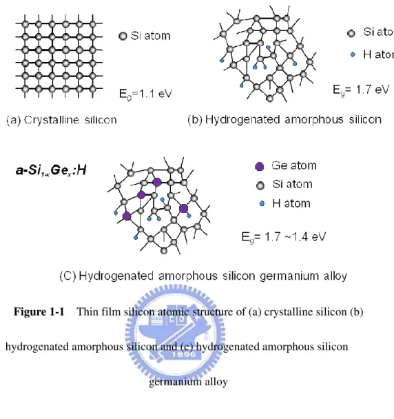
Figure 1-1 Thin film silicon atomic structure of (a) crystalline silicon (b) hydrogenated
amorphous silicon and (c) hydrogenated amorphous silicon germanium alloy.
Figure 1-2 Structure of thin film single junction solar cell.
Figure 1-3 Schematic of air mass
Figure 1-4 Schematic representation of the rf PECVD system.
Figure 2-1 The volume of a-Si1-xGex:H that contributes to conductivity between two silver
contacts.
Figure 2-2 Photo energy ( h ω) as function of the
(
αhω)
12 and the tauc band gap valueFigure 3-1 Variations in germanium concentration and deposition rate (RD) of a-Si1-xGex:H
alloy with germane flow rate.
Figure 3-2 Variation in photo to dark conductivity ratio with germane flow rate
Figure 3-3 Relationship between deposition rate and hydrogen dilution ratio (H2 / (GeH4 +
SiH4)) of a-Si1-xGex:H alloy films with two different Xg values.
Figure 3-4 Effect of hydrogen dilution ratio on the optical bandgap (Eg) with three Xg
values.
Figure 3-5 Variations in photo conductivity (σph) and dark conductivity (σd) with hydrogen
Figure 3-7 Relationship between germanium content and hydrogen dilution ratio.
Figure 3-8 Hydrogen bonding configurations measured by FTIR. Wavenumbers 1890, 1980,
2000, 2090 cm-1 arecorresponding to GeH, GeH2, SiH, and SiH2, respectively.
Figure 3-9 Hydrogen bonding configurations measured by FTIR. (a) GeH2 to GeH ratio, (b)
SiH2 to SiH ratio, black arrow in figure3-9(a) presents that GeH2 to GeH ratio is infinity as H2
dilution ratio is 0.
Figure 3-10 (a) Deposition rate and (b) optical bandgap with varying h2 dilution ratio.
Black square and blue triangle correspond to a-Si1-xGex:H materials prepared with power
values at 20W and 30W, respectively.
Figure 3-11 Variations in photo conductivity (σph) and dark conductivity (σd) with
hydrogen dilution ratio. Black square and blue triangle are corresponding to powers 20 and 30 W respectively. Open and closed symbols correspond to photo and dark conductivity.
Figure 3-12 Hydrogen bonding configurations measured by FTIR. (a) GeH2 to GeH ratio,
(b) SiH2 to SiH ratio, black arrow in figure3-12(a) presents that GeH2 to GeH ratio is infinity
as H2 dilution ratio is 0.
Figure 3-13 Variations in photo conductivity (σph) and dark conductivity (σd) with hydrogen
dilution ratio. Black square and blue triangle are corresponding to electrode spacing (E/S) 20 and 22 mm, respectively. Open and closed symbols
correspond to photo and dark conductivity. As E/S at 20 mm, powder generated when H2
dilution ratio is equal to 8.
Figure 3-14 Variation in photo-to-dark conductivity ratio with hydrogen dilution ratio.
Black square and blue triangle are corresponding to electrode spacing (E/S) 20 and 22 mm, respectively.
Figure 3-15 a-Si1-xGex:H single junction structure.
Figure 3-16 a-Si1-xGex:H single junction solar cell I-V curve and cell performances. (a) Xg
is equal to 8.3 % and (b) Xg is equal to 16.7 %
Chapter 1
Introduction
1.1. Silicon thin film solar cell technologies
Due to the low cost and large area producibility, a-Si:H solar cells have attracted much attentions these years. It is well known that single junction a-Si:H devices perform well only in the blue end of the solar spectrum but miss much of the red-wavelength region. The other problem in a-Si based solar cells is a decline in efficiency due to an increase of metastable defects in the photovoltaic layer during light irradiation, or the so-called the Staebler–Wronski effect [1].
The way to overcome these problems is by using a tandem solar cell. In a tandem solar cell, structure based on multiple devices in tandem use various a-Si:H alloys to maximize the use of the solar spectrum. The long wavelength regions of the solar spectrum can be utilized by using a low bandgap material like hydrogenated amorphous silicon germanium alloy. Hydrogenated amorphous silicon germanium (a-Si1-xGex:H) alloy is a promising material for the photovoltaic layer of multijunction
solar cells because of their optical gap (Eg) can be narrowed by changing germanium
content in the alloy. Multijunction solar cells incorporating an a-SiGe:H alloy as the bottom photovoltaic layer have exhibited performance improvement. Since the thickness of each photosensitive layer in a tandem structure is less than that in a single
junction solar cell, the light-induced degradation effects are smaller. Also, optical bandgap of a-Si1-xGex:H can easily be tuned to match the wavelength region of solar
radiation spectrum. Development of low bandgap and highly photosensitive a-SiGe:H alloy has become a major task for fabrication of tandem amorphous silicon solar cell with higher efficiency and better stability [2].
1.2. Amorphous silicon and Amorphous silicon alloy
Hydrogenated amorphous silicon (a-Si:H) is the non-crystalline allotropic form of silicon. It can be deposited as thin film onto a variety of substrates at low temperatures. Silicon is a four-fold coordinated atom that is normally tetrahedrally bonded to four neighboring silicon atoms. In crystalline silicon this tetrahedral structure is continued over a large range, forming a well-ordered lattice (crystal), as shown in figure 1-1(a).
In amorphous silicon this long range order is not present and the atoms form a continuous random network, as shown in figure 1-1(b). Not all the atoms within amorphous silicon are four-fold coordinated. Due to the disordered nature of the material, some atoms have dangling bonds. These dangling bonds present as defects in the
Figure 1-1 Thin film silicon atomic structure of (a) crystalline silicon (b)
hydrogenated amorphous silicon and (c) hydrogenated amorphous silicon germanium alloy
silicon random network, which cause anomalous electrical behavior. If desired, the material can be passivated by hydrogen which bonds to the dangling bond to reduce the dangling bond density by several orders of magnitude. In general, there exists about 10 at.% hydrogen in hydrogenated amorphous silicon thin film. Hydrogenated amorphous silicon has a sufficiently low amount of defects to be used within devices. However, the hydrogen is unfortunately associated with light-induced degradation of the material, termed the Staebler-Wronski effect.
Amorphous silicon alloys are widely used in thin film solar cell technologies, such as a-Si1-xGex or a-S1-xiCx:H. Structure of amorphous silicon germanium alloy is
shown in figure 1-1(c). Introduction of carbon or germanium adds extra freedom to controlling the properties of the material. Increasing concentration of germanium in the alloy narrows the electric gap between conduction and valence band (called bandgap) in order to potentially increase the light efficiency of solar cells made with amorphous silicon germanium layers. On the other hand, the electric properties as a semiconductor (mainly electron mobility), are badly affected by the increasing content of germanium in the alloy, due to the increased disorder in the atomic network.
One advantage is that a-Si or its alloys can be deposited at very low temperatures. This allows for deposition on not only glass, but plastic as well, making it a candidate for a roll-to-roll processing technique. Another advantage is that a-Si can be deposited over large areas by PECVD.
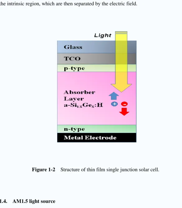
1.3. p-i-n structure
Typically, amorphous silicon thin film cells use a p-i-n structure, as shown in figure 1-2. The basic scenario is as follows: A three-layer sandwich is created, with a middle intrinsic (i-type or undoped) layer between an n-type layer and a p-type layer. This geometry sets up an electric field between the p- and n-type regions that stretches
across the middle intrinsic resistive region. Light generates free electrons and holes in the intrinsic region, which are then separated by the electric field.
Figure 1-2 Structure of thin film single junction solar cell.
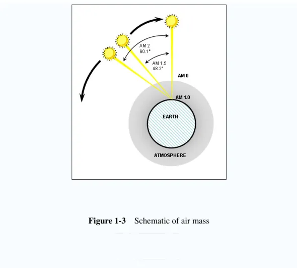
1.4. AM1.5 light source
Solar radiation closely matches a black body radiator at 5,800 K. As the sunlight travels though the atmosphere, chemicals react with the sunlight and absorb certain wavelengths. Perhaps the best known example is the stripping of ultraviolet light by ozone in the upper atmosphere, which drastically reduces the amount of short wavelength light reaching the Earth's surface. A more active component of this
process is water vapor, which results in a wide variety of absorption bands at many wavelengths, while molecular nitrogen, oxygen and carbon dioxide add to this process.
Atmospheric scattering also plays a role by removing higher frequencies from direct sunlight and scattering it about the sky. The greater the distance of atmosphere the sunlight travels through, the greater this effect, which is why the sky looks pink at sundown when the sunlight is traveling obliquely through the atmosphere.
For a thickness lo of the atmosphere, the path length l through the atmosphere for solar
radiation incident at angle θ relative to the normal to the Earth's surface is
l = lo / cos θ
The ratio l / lo is the air mass coefficient.
As shown in figure 1-3, the spectrum outside the atmosphere, the 5,800 K black body, is referred to as "AM0", meaning "zero atmospheres". Cells used for space power applications, like those on communications satellites are generally characterized using AM0.
Figure 1-3 Schematic of air mass
The spectrum after traveling through the atmosphere to sea level with the sun directly overhead is referred to as "AM1". This means "one atmosphere". Conveniently, silicon solar cells are not very sensitive to the portions of the spectrum lost in the atmosphere. Since solar cell development is concentrated in the United States, Europe and Japan, an AM number representing the spectrum at mid-latitudes is much more common. "AM1.5", 1.5 atmosphere thicknesses, corresponds to a solar zenith angle of 48°, and is almost universally used to characterize solar panels.
1.5. Staebler–Wronski effect
The Staebler-Wronski Effect (SWE) refers to light-induced metastable changes in the properties of hydrogenated amorphous silicon. The defect density of hydrogenated amorphous silicon (a-Si:H) increases with light exposure, causing an increase in the recombination current and leading to the reduction in the sunlight to electricity conversion efficiency. Such phonomenon was discovered by D. L. Staebler and C. R. Wronski in 1977. They showed that the photoconductivity of hydrogenated amorphous silicon can be reduced significantly by prolonged illumination with intense light. However, by heating the samples to above 150 °C, they could reverse the effect.
The efficiency of an amorphous silicon solar cell typically drops during the first six months of operation. This drop may be in the range from 10% up to 30% depending on the material quality and device design. After this initial drop, the effect reaches equilibrium and causes little further degradation. Most commercially available a-Si modules have SWE degradation in the 10 to 15% range and suppliers typically specify efficiency based on performance after the SWE degradation has stabilized. In a typical amorphous silicon solar cell the efficiency is reduced by up to 30% in the first 6 months as a result of the Staebler–Wronski effect, and the fill
factor falls from over 0.7 to about 0.6. This light induced degradation is the major disadvantage of amorphous silicon as a photovoltaic material.
1.6. PECVD
Plasma enhanced chemical vapor deposition (PECVD) system is widely used to fabricate silicon thin film solar cell. Deposition of silicon thin film bye PECVD is a low temperature process which is usually less than 300℃. Therefore, silicon thin film can deposit onto variety of substrates such as glass, stainless steel, or plastic substrate. Comparing to the silicon wafer substrate, employing the above substrates is a good point of view to industry for large scale productions and cost reduction. Besides, doping and alloying are easier by using PECVD method. For example, introducing source gases of SiH4 and B2H6 or SiH4 and PH3 mixture, doping layers can
be easily deposited onto different substrates.
1.7. Motivation
As mention in 1.1, hydrogenated amorphous silicon germanium (a-SiGe:H) alloys are promising materials for the photovoltaic layer of multijunction solar cells because their optical bandgap (Eg) can be narrowed by adding germanium. It is necessary to
cell. But the electric properties of a-SiGe:H alloy deteriorate sharply and photoelectric response becomes poor below an optical gap of about 1.5 eV. Deterioration of electric properties is attributed to the microstructural defects of alloy films. Recent evidences [3, 4] confirm that the degradation of electric properties of a-SiGe:H alloy film with germanium content greater than 0.2 is inevitable due to the column-like microstructural growth. Microstructural defects can be removed to certain extent by
proper use of hydrogen dilution of source gases [5]. In this work, variations in electric and structural properties of a-Si1-xGex:H alloy
under systematic variation in hydrogen dilution with RF power, germane-to-silane ratio, and electrode spacings have been studied in detail. This thesis presents not only material properties but also the performance of devices. Single-junction solar cells have been fabricated to investigate the dependence of device performance on different film properties.
1.8. Thesis outline
This thesis is organized into the following chapters:
In chapter 1, a brief overview of thin film solar cell technology is introduced to describe its advantages and bottlenecks. The motivation of the study is also
In chapter 2, the process flow of the xeperiment is introduced. The measurement methods are also showed here in detail.
Chapter 3 shows the dependence of material properties and device performance on various conditions with different hydrogen dilution ratios.
Chapter 4 discusses the results from chapter 3. The effect and the dependence of the material properties on different conditions will be explained here.
In chapter 5, the results of our experiments in chapter 3 and discussions in chapter 4 are concluded.
Chapter 2
Experimental Details
2.1. Experimental introductions
Hydrogenated amorphous silicon germanium films were deposited using pure
SiH4 and pure GeH4 mixture with H2 dilution by radio frequency (27.12 MHz) plasma
enhanced chemical vapor deposition (PECVD) system. Doping layers were prepared by using B2H6 or PH3 with pure SiH4 or with H2 dilution. Prior to
depositing all the samples, the chamber was introduced with NF3 and Ar to clean the
chamber. Corning Eagle2000 glass and c-si wafer substrate were clean by KG Cleaner and RCA standard cleaning process, respectively. All the samples were started to be deposited after background pressure of 5 * 10-4 Pa is reached. In this study, a-SiGe:H alloys were prepared simultaneously on 5cm * 5cm Corning Eagle 2000 glass and 1.5cm * 1.5cm c-si wafer. The films grew on glass substrate were used to analysis optoelectrial properties and the films grew on c-si wafer were used to determine the hydrogen bonding configuration.
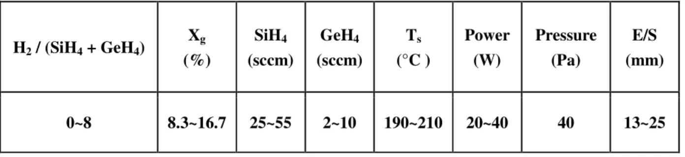
The complete range of deposition conditions include: substrate temperature (TS):
GeH4 / (GeH4+SiH4)) : 8.3-16.7 %, and hydrogen dilution ratio (H2 / ((GeH4+SiH4))) :
0~8. All above deposition parameters are listed in Table I.
H2 / (SiH4 + GeH4) Xg (%) SiH4 (sccm) GeH4 (sccm) Ts (°C ) Power (W) Pressure (Pa) E/S (mm) 0~8 8.3~16.7 25~55 2~10 190~210 20~40 40 13~25
Table I Experimental details
2.2. Measurement Method
a-SiGe:H alloys were prepared simultaneously on 5cm * 5cm Corning Eagle 2000 glass and 1.5cm * 1.5cm c-si wafer. The thickness of the films was determined by Ellipsometer and α-stepper. After depositing a-SiGe:H film on the glass, silver contacts with width-to-length ratio of 0.05 were coated on the film by evaporator. Photo and dark conductivity measurements were carried out by using a Keithley model 236 electrometer. Before each measurement, samples were annealed at 150 °C in vacuum. The photoconductivity is measured under AM1.5 light spectrum. The Tauc bandgap is taken from the fitting of E versus (αhν)1/2curve, in which α is calculated by the method of interference-free determination of optical absorption coefficient [6] on the raw data of transmission. The films grown on the c-si wafer
were used to determine hydrogen bonding configurations by Fourier transform infrared spectroscopy (FTIR) [7]. Germanium and silicon atomic concentration in the a-SiGe:H alloy were measured by X-ray photoelectron spectroscopy (XPS) system. Quantum efficiency spectra of solar cells were measured using a lock-in detection technique under modulated monochromatic light illumination superimposed on an AM1.5 bias light.
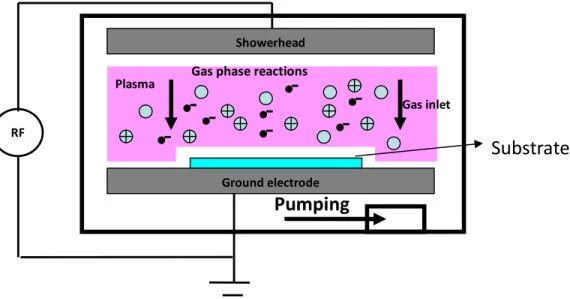
2.3. Radio-Frequency plasma enhanced chemical vapor deposition
Plasma-enhanced chemical vapor deposition (PECVD) is a common technique used for the manufacturing of most microeletronic devices. The role of the plasma is to provide a source of energy to dissociate silicon bearing gas, which is usually silane (SiH4). This is done by collisions with electrons, which originate as secondary
electrons in the plasma to build up their energy by acceleration in an electric field. The growth of an a-Si1-xGex:H film is accomplished by attaching reactive particles of
dissociated silane and germane molecules, call radicals, to the surface, as sketched in Figure 1-4
Figure 1-4 Schematic representation of the rf PECVD system.
Plasma dissociation process in reactive chamber can generate variety of radicals including SiH2 and GeH2 from SiH4, GeH4, and H2 gas mixture. These two
radicals have higher sticking coefficients than other radicals and they would incorporated directly onto the hydrogen terminated surface without finding potential favorable growth site. [3]. Besides, the contribution of these radical to the growth results in poor quality film, and therefore the presence of these radicals in the plasma should to be avoided.
2.4. Conductivity analysis
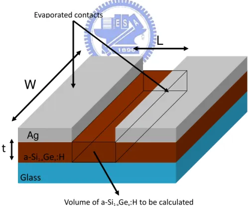
In order to investigate the conductivity of the a-Si1-xGex:H alloy, metal contacts
were deposited onto the film by thermal evaporation. Conductivity is calculated by equation (1), where V and I are the bias voltage and measured current, respectively.
RF
Pumping
PlasmaSubstrate
Gas inlet Ground electrodeGas phase reactions
The volume of material contributing to conductivity is determined by the width (W), length (L), and thickness (t) of a cuboid located between the conducting contacts used to probe the sample in the Figure 2-2.
A prepared a-Si1-xGex:H film with silver contacts is show in figure 2-2.
Photoconductivity was measured by AM1.5 light spectrum with power at 100mw/cm2. For the amorphous silicon germanium film, the thickness is about 600 nm.
Figure 2-1 The volume of a-Si1-xGex:H that contributes to conductivity between two
silver contacts. Evaporated contacts
Glass
a-Si
1-xGe
x:H
Ag
W
t
L
Volume of a-Si1-xGex:H to be calculated
(1)
t
1
W
L
V
I
=
σ
2.5. Determination of optical bandgap
The optical bandgap of thin film use UV/VIS/NIR spectrometers to measure transmission (T) spectra were carried out between 200nm and 1.3 µm in the step of 2 nm. Calculating optical bandgap (Eg) has to use transmission spectra and thickness
of thin film in equation (2).
(
α
h
ω
)
12=
c
(
h
ω
-
E
opt)
(2)
Figure -3 shows the photo energy ( h ω) as function of the
(
αhω)
12. Theband gap value can be determined from the expanding linear region line intercepts a-axis. 1.0 1.5 2.0 2.5 3.0 3.5 0.00 0.02 0.04 0.06 0.08 0.10 0.12 (αααα hωωωω ) 1 /2 hωωωω (ev)
band gap value
Figure 2-2 Photo energy ( h ω) as function of the
(
αhω)
12 and the tauc band gapChapter 3
Result
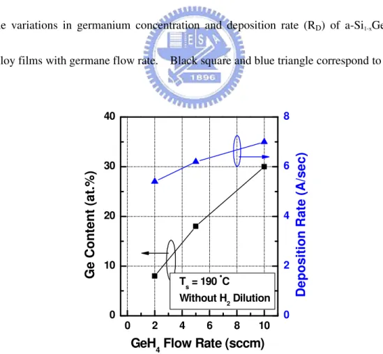
3.1. Effect of the germane flow rate
Amorphous silicon germanium films were prepared with varying germane flow rates. Germane flow rate increases from 2 to 10 sccm. Deposition time and pressure for all the samples are fixed at 900 seconds and 40 Pa. Figure 3-1 Shows the variations in germanium concentration and deposition rate (RD) of a-Si1-xGex:H
alloy films with germane flow rate. Black square and blue triangle correspond to
Figure 3-1 Variations in germanium concentration and deposition rate (RD) of
0 2 4 6 8 10 0 10 20 30 40
GeH
4Flow Rate (sccm)
G
e
C
o
n
te
n
t
(a
t.
%
)
Ts = 190 °°°° C Without H2 Dilution 0 2 4 6 8D
e
p
o
s
it
io
n
R
a
te
(
A
/s
e
c
)
a-Si1-xGex:H alloy with germane flow rate.
germanium concentration and deposition rate. Figure 3-1 shows that, as the flow rate of germane increases from 2 to 10 sccm, the deposition rate and germanium concentration increase with increasing germane flow rate. It can be observed from figure 3-1 that deposition rate are higher for a-Si1-xGex:H film deposited at higher
germane flow rate. Germanium atomic concentration in a-Si1-xGex:H film can reach
to 30% when germane flow rate is 10 sccm. And only 8 % of germanium atomic concentration in a-Si1-xGex:H alloy as film was prepared with 2 sccm of germane flow
rate.
The variation in photo to dark conductivity ratio (σph /σdark ) with germane
flow rate is shown in figure 3-2.
0 2 4 6 8 10
10
210
310
410
5σσσσ
p h/
σσσσ
dR
a
ti
o
Figure 3-2 Variation in photo to dark conductivity ratio with germane flow rate
From figure 2, increasing germane flow rate further decreases the photo to dark ratio from 104 to 103. This means film’s optoelectronic properties were degraded with the increase in germane flow rate.
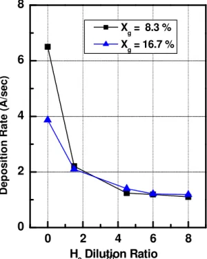
3.2. Effect of the hydrogen flow rate
3.2.1. Deposition rate and optical bandgap
Amorphous silicon germanium films were prepared with varying hydrogen flow rates. This has been repeated for two different gas phase ratio of germane, Xg (Xg =
GeH4 / (GeH4 + SiH4), values. Change the Xg value from 8.3 % to 16.7 % by
decreasing silane flow rate. Pressure for all samples is fixed at 40 Pa.
0 2 4 6 8 Xg = 8.3 % Xg = 16.7 % D e p o s it io n R a te ( A /s e c )
Figure 3-3 Relationship between deposition rate and hydrogen dilution ratio (H2 /
(GeH4 + SiH4)) of a-Si1-xGex:H alloy films with two different Xg values.
Figure 3-3 illustrates the relationship between deposition rate and hydrogen dilution ratio (H2 / (GeH4 + SiH4)) of a-Si1-xGex:H alloy films with two different Xg
values. Black circle and blue rhombus correspond to Xg value 8.3 % and 16.7 %.
The deposition rates with two different Xg values in figure 3-3 demonstrate that, with
the increase in hydrogen dilution ratio from 0 to 9, the deposition rate decreases sharply and with a further rise in dilution ratio the rate of decrease in deposition rate become slow. For the hydrogen dilution ratio larger than 3, the RD for two Xg values
are almost the same.
The effect of hydrogen dilution ratio on the optical bandgap (Eg) with three Xg
values is presented in figure 3-4 which represents initial Eg of the alloy films
decreases rapidly due to the increase in hydrogen dilution ratio from 0 to 5 and Eopt
that it varies slowly thereafter. At any hydrogen ratio, Eg values are lower for films
deposited under higher Xg value. Eg decreases from 1.58 to 1.48 eV with the change
Figure 3-4 Effect of hydrogen dilution ratio on the optical bandgap (Eg) with three
Xg values.
3.2.2. Electronic properties
The variations in photo conductivity (σph) and dark conductivity (σd) with the
hydrogen dilution ratio are shown in figure 3-5. Black circle and blue rhombus correspond to a-SiGe:H materials prepared at gas phase ratio of germane values 8.3 % and 16.7 % respectively. Open and closed symbols correspond to photo and dark conductivity. From figure 3-5, photo conductivity increases with increasing
0 2 4 6 8 1.4 1.6 1.8
16.7%
11.1%
H
2Dilution Ratio
E
g(
e
V
)
X
g
8.3 %
ratio the photo conductivity decrease for the material prepared under Xg at 8.3%.
The photo conductivity decreases as hydrogen dilution ratio larger than 6 for the little Xg value, but photo conductivity are higher for films deposited at lower gas phase
ratio of germane for all hydrogen dilution ratios. For the dark conductivity, the trend is converse compare to the case of photo conductivity. Dark conductivity is higher for films deposited at higher gas phase ratio of germane for all hydrogen dilution ratios. With the further increase in hydrogen dilution ratios, dark conductivity gradually increases for the samples prepared under higher Xg value. But the films
with the lower Xg value keep the constant as hydrogen dilution ratio lower than 6.
An interesting point for a-SiGe:H alloy prepared under lower Xg value, namely Xg =
8.3%, is that the dark conductivity sharply increases and photo conductivity sharply decreases when hydrogen dilution ratio larger than 6. From figure 3-5, high gas phase ratio of germane and deteriorates the film properties. It also can be observed from figure 3-6, photo to dark ratio increases significantly with increasing hydrogen dilution ratio from 0 to 6 in the case of lower germane gas phase ratio. With a further increase in hydrogen dilution ratio the photo to dark conductivity ration decreases for the materials with lower Xg value. But in the case of higher germane
hydrogen dilution ratios. Figure 6 indicates that hydrogen cannot improve film’s properties when the a-SiGe:H alloy prepared under higher Xg value.
0 2 4 6 8 10-11 10-10 10-9 10-8 10-7 10-6 10-5 10-4
σ
p h ( S c m -1 ) Xg = 8.3 % Xg = 16.7 %σ
d ( S c m -1 )H
2Dilution Ratio
Figure 3-5 Variations in photo conductivity (σph) and dark conductivity (σd) with
Figure 3-6 Variation in photo-to dark conductivity ratio with hydrogen dilution ratio. 0 2 4 6 8 102 103 104 105 106 X g = 8.3 % X g = 16.7 %
σσσσ
p
h
/
σσσσ
d
R
a
ti
o
H
2Dilution Ratio
3.2.3 Structural properties
Figure 3-7 shows the relationship between germanium atomic concentration and hydrogen dilution ratio. The Xg value keeps at 8.3 % for all samples. Initially germanium atomic concentrationincreases rapidly due to the increase in hydrogen dilution ratio from 0 to 1 and germanium atomic concentration that it varies slowly thereafter. Figure 7 shows that germanium atomic concentration in a-SiGe:H film can reach to 24 % when hydrogen dilution ratio is 2. It may be noticed in figure 7 that germanium atomic concentration increases by 5 % of magnitude with the increase in hydrogen dilution ratio.
0.0 0.5 1.0 1.5 2.0 16 18 20 22 24 26 28 30 Xg = 8.3 %
G
e
C
o
n
te
n
t
(a
t.
%
)
H
2Dilution Ratio
Figure 3-8 shows the hydrogen bonding configurations measured by FTIR. Wavenumbers 1890, 1980, 2000, 2090 cm-1 arecorresponding to GeH, GeH2, SiH,
and SiH2, respectively. German to silane ratio was fixed at 16.7 %. It may be
observed from figure 3-8 that SiH2 radical sharply decreases as hydrogen dilution
ration increase from 0 to 1.5. It means introducing hydrogen can decrease the dihydride (SiH2) content in the a-Si1-xGex:H alloy network.
1800 1900 2000 2100 2200
Wavenumber (cm
-1)
0
1.5
SiH2 GeH2 SiH26
GeH28
H
fF
T
IR
I
n
te
n
s
it
y
(
a
.u
.)
Xg = 16.7 %Spectra GeH GeH 2 SiH SiH2Figure 3-8 Hydrogen bonding configurations measured by FTIR. Wavenumbers
1890, 1980, 2000, 2090 cm-1 are corresponding to GeH, GeH2, SiH, and SiH2,
Figure 3-9 shows the [Si-H2] / [Si-H] and [Ge-H2] / [Ge-H] of a-SiGe:H samples
with various hydrogen dilution ratio. Black square and blue triangle correspond to a-Si1-xGex:H materials prepared with germane to silane ratio values at 8.3 % and 16.7
%, respectively. In figure 3-9(a) and 3-9b(b), the biggest ratio of [Si-H2] / [Si-H]
and [Ge-H2] / [Ge-H] appear as hydrogen dilution ratio is zero. From figure 3-9(a),
[Ge-H2] / [Ge-H] sharply decreases with increasing hydrogen dilution ratio from 0 to
1.5. [Ge-H2] / [Ge-H] is higher for films deposited at higher germane to silane ratio
for all hydrogen dilution ratios. For the [Si-H2] / [Si-H], the trend is as same as the
case of [Ge-H2] / [Ge-H]. From figure 3-9(b), [Si-H2] / [Si-H] sharply decreases with
increasing hydrogen dilution ratio from 0 to 1.5. With a further increase in hydrogen dilution ratio, the [Si-H2] / [Si-H] gradually increases for the material prepared for
two different Xg value. Figure 3-9 indicates that hydrogen dilution ratio plays an
important role in a-Si1-xGex:H alloy because it may influence the ratio of [Si-H2] /
[Si-H] and [Ge-H2] / [Ge-H]. And the amount of these two radicals, [Si-H2] and
[Ge-H2], in the film make the crucial impact on the properties of the a-Si1-xGex:H
Figure 3-9
Hydrogen bonding configurations measured by FTIR. (a) GeH2 to GeH
ratio, (b) SiH2 to SiH ratio, black arrow in figure3-9(a) presents that GeH2 to GeH
ratio is infinity as H2 dilution ratio is 0.
0 1 2 3 4 5 6 7 8 0.0 0.5 1.0 1.5 0 1 2 3 4 5 6
S
iH
2/
S
iH
H
2Dilution Ratio
G
e
H
2/
G
e
H
X g = 8.3 % Xg = 16.3 %FTIR
(a)(b)
3.3. Effect of power
3.3.1. Deposition rate and optical bandgap
Hydrogenated amorphous silicon germanium films were prepared with varying hydrogen flow rates. This has been repeated for two different powers. Pressure
and germane-to-silane ratio for all samples are fixed at 40 Pa and 8.3 %. Figure 3-10(a) illustrates the relationship between deposition rate and hydrogen dilution ratio of a-SiGe:H alloy films for two different power densities. Black square and blue triangle correspond to power value 20 and 30 W. The deposition rates with two different Powers values in figure 3-10(a) demonstrate that, with the increase in hydrogen dilution ratio from 0 to 1.5, the deposition rate decreases sharply and with a further rise in H2 dilution ratio the rate of decrease in deposition rate become slow.
For the hydrogen dilution ratio larger than 3, the deposition rate for the samples prepared under two different powers are almost the same in figure 3-10(a).
The effect of hydrogen dilution ratio on the optical bandgap (Eg) with different
power values is presented in figure 3-10(b) which represents initial Eg of the films
decreases rapidly due to the increase in hydrogen dilution ratio from 0 to 1.5 and Eg
for films deposited under two different powers. Eg decreases from 1.7 to 1.58 eV
with the change in hydrogen ratio from 0 to 8.
Figure 3-10 (a) Deposition rate and (b) optical bandgap with varying h2 dilution
ratio. Black square and blue triangle correspond to a-Si1-xGex:H materials prepared
with power values at 20W and 30W, respectively.
0 2 4 6 8 1.4 1.6 1.8 0 2 4 6 8
E
g(
e
V
)
H
2Dilution Ratio
power = 20 (W) Power = 30 (W)D
e
p
.
R
a
te
(
A
/s
e
c
)
(b)
(a)
3.3.2. Optoelectronic properties
The variations in photo conductivity (σph) and dark conductivity (σd) with the
hydrogen dilution ratio are shown in figure 3-11. The Xg value still keeps at 8.3 %
for all samples. Black square and blue triangle correspond to powers 20 and 30 W respectively. Open and closed symbols correspond to photo and dark conductivity.
Figure 3-11 Variations in photo conductivity (σph) and dark conductivity (σd) with
hydrogen dilution ratio. Black square and blue triangle are corresponding to powers 20 and 30 W respectively. Open and closed symbols correspond to photo and dark conductivity. 0 2 4 6 8 10-11 10-10 10-9 10-8 10-7 10-6 10-5 10-4
σ
p h(
S
c
m
-1
)
σ
d(
S
c
m
-1
)
H
2Dilution Ratio
Power = 20 (W) Power = 30 (W)From figure 3-11, photo conductivity increases with increasing hydrogen dilution ratio from 0 to 4.5 for two different powers. Photo conductivity is higher for films deposited at higher power density for all hydrogen dilution ratios. Dark conductivity is almost the same for films deposited at two different powers for all hydrogen dilution ratios. From figure 3-11, high power density can improve the film properties.
3.3.3. Structural properties
Figure 3-12 shows the [Si-H2] / [Si-H] and [Ge-H2] / [Ge-H] of a-S1-xiGex:H
samples with various hydrogen dilution ratio. Black square and blue triangle correspond to powers 20 and 30 W, respectively. In figure 3-12(a) and figure 3-12(b), the largest ratio of [Si-H2] / [Si-H] and [Ge-H2] / [Ge-H] appear as samples
prepared without any hydrogen dilutions. From figure 3-12(a), [Ge-H2] / [Ge-H]
sharply decreases with increasing hydrogen dilution ratio from 0 to 1.5 for the samples prepared under lower power. With the further increase in hydrogen dilution ratio, the [Ge-H2] / [Ge-H] gradually increases for the material prepared for two
different power values. But for the films prepared by higher power, the [Ge-H2] /
[Ge-H] ratio at zero hydrogen dilution ratio is the smallest contrast to other samples. From figure 3-12(b), [Si-H2] / [Si-H] sharply decreases with increasing hydrogen
dilution ratio from 0 to 1.5. Figure 3-12 indicates that power also plays an important role in a-Si1-xGex:H alloy because it may influence the ratios of [Si-H2] / [Si-H] and
[Ge-H2] / [Ge-H].
Figure 3-12
Hydrogen bonding configurations measured by FTIR. (a) GeH2 to
GeH ratio, (b) SiH2 to SiH ratio, black arrow in figure3-12(a) presents that GeH2 to
GeH ratio is infinity as H2 dilution ratio is 0.
0 2 4 6 8 0.0 0.5 1.0 1.5 0 2 4 6 8 0 1 2 3
S
iH
2/
S
iH
H
2Dilution Ratio
Power = 20 (W) Power = 30 (W)G
e
H
2/
G
e
H
FTIR
(a)
(b)
3.4. Effect of electrode spacing
The variations in photo conductivity (σph) and dark conductivity (σd) with the
hydrogen dilution ratio are shown in figure 3-13. This has been repeated for two different electrode spacings, namely E/S. Pressure and germane-to-silane ratio for
all samples are fixed at 40Pa and 8.3 %. Black square and blue triangle correspond to a-Si1-xGeX:H materials prepared at electrode spcings values 20 mm and 22 mm,
respectively. Open and closed symbols correspond to photo and dark conductivity. From figure 3-13, photo conductivity increases with increasing hydrogen dilution ratio from 0 to 4.5. With the further increase in hydrogen dilution ratio the photo conductivity decrease for the material prepared under E/S at 20 and 22 mm. The photo conductivity decreases as hydrogen dilution ratio larger than 4.5 both for two different E/S values. With the further increase in hydrogen dilution ratios, dark conductivity gradually increases for the samples prepared under lower E/S value. But the dark conductivity for the films with the higher E/S value keeps the constant at all hydrogen dilution ratios. From figure 3-13, high hydrogen dilution ratio will degrade the film’s properties or generate powders as samples prepared under lower E/S value, as shown in figure 3-13. The same trend can also be observed from figure 3-14, photo-to-dark conductivity ratios increase significantly with increasing
hydrogen dilution ratio from 0 to 4.5 in two different cases. With a further increase in hydrogen dilution ratio the photo to dark conductivity ration decreases for the materials. Figure 3-14 indicates that too many hydrogen dilution ratios cannot improve film’s properties as the a-Si1-xGex:H alloy prepared for two E/S values.
Figure 3-13 Variations in photo conductivity (σph) and dark conductivity (σd) with
hydrogen dilution ratio. Black square and blue triangle are corresponding to electrode spacing (E/S) 20 and 22 mm, respectively. Open and closed symbols correspond to photo and dark conductivity. As E/S at 20 mm, powder generated
0 2 4 6 8 10-11 10-10 10-9 10-8 10-7 10-6 10-5 10-4
σ
p h ( S c m -1 )σ
d ( S c m -1 )H
2Dilution Ratio
E/S = 20 mm E/S = 22 mm Powder FormationFigure 3-14 Variation in photo-to-dark conductivity ratio with hydrogen dilution
ratio. Black square and blue triangle are corresponding to electrode spacing (E/S) 20 and 22 mm, respectively. 0 2 4 6 8 103 104 105 106
σσσσ
p
h
/
σσσσ
d
R
a
ti
o
H
2Dilution Ratio
E/S = 20 mm E/S = 22 mm3.5. Impact on devices
In order to investigate the effect of i layer on a-Si1-xGex:H device performance,
two cells were prepared under two different germanium contents in i layer. The structure of cells was shown in figure 3-15. One of them was prepared under the Xg
value at 8.3 % and the other one was at 16.7 %. I-V curve and cell performance were shown in figure 3-16. From figure 3-16(a) and figure 3-16(b), open circuit voltage is higher for the cell prepared under lower Xg value. The short circuit
current density decreases from 14.70 mA/cm2 to 13.76 mA/cm2 by decreasing the Xg
value from 16.7 % to 8.3 %. Although increasing the Xg value can increase the short
circuit current, but the higher Xg value will cause the reduction of the fill factor from
60.60 % to 48.71 % and also deteriorate the cell efficiency from 6.33 % to 4.85 %. Figure 3-17. shows the quantum efficiency spectra of two cells measured at short circuit under AM1.5 bias illumination.. Figure 3-17. not only compares the external quantum efficiency of two different cells but also amorphous silicon solar cell. In figure 3-17, the spectral sensitivity of solar cell extends systematically towards longer wavelengths as the Xg value increases in i layer in the range from
8.3% to 16.7 %. On the other hand, a decrease in Q.E. in the short wavelength region is also observed when Xg value is at 8.3 % compare to the amorphous silicon
solar cell. The higher Xg value (16.7 %) results in a further drop in the short
wavelength response.
Figure 3-16 a-Si1-xGex:H single junction solar cell I-V curve and cell performances.
(a) Xg is equal to 8.3 % and (b) Xg is equal to 16.7 %
Figure 3-17 Quantum efficiency for a-Si:H and a-Si1-xGex:H solar cells
-1.0 -0.8 -0.6 -0.4 -0.2 0.0 0.2 0.4 0.6 0.8 1.0 -15 -12 -9 -6 -3 0 3 6 9 12 15 -1.0 -0.8 -0.6 -0.4 -0.2 0.0 0.2 0.4 0.6 0.8 1.0 -15 -12 -9 -6 -3 0 3 6 9 12 15 C u rr e n t D e n s it y ( m A /c m 2) Voltage ( V ) Xg = 16.7 % VO C= 0.68 ( V ) J sc= 14.70 ( m A/cm 2 ) F.F. = 48.71% Efficiency = 4.85% -1 .0 -0 .8 -0 .6 -0 .4 -0 .2 0 .0 0 .2 0 .4 0 .6 0 .8 1 .0 -1 5 -1 2 -9 -6 -3 0 3 6 9 1 2 1 5 -1 .0 -0 .8 -0 .6 -0 .4 -0 .2 0 .0 0 .2 0 .4 0 .6 0 .8 1 .0 -1 5 -1 2 -9 -6 -3 0 3 6 9 1 2 1 5 C u rr e n t D e n s it y ( m A /c m 2) V o lta g e ( V ) Xg = 8 .3 % VO C= 0 .7 6 ( V ) Js c= 1 3 .7 6 ( m A /c m2 ) F .F . = 6 0 .5 0 % E ffic ie n c y = 6 .3 3 %
(a)
(b)
300 400 500 600 700 800 900 0 10 20 30 40 50 60 70 80 90 100 0 10 20 30 40 50 60 70 80 90 100 Xg = 8.3 % Xg = 16.7 % Wavelength ( nm ) Q .E . [% ] a-SiChapter 4
Discussion
4.1. Deposition rate
It may be recalled from figures 3-3 that the effect of variation in hydrogen
dilution ratio on deposition rate is very prominent in the low-dilution ratio region (< 1.5) whereas in the high-dilution ratio region deposition rate is nearly independent of the degree of dilution ration and germane-to-silane ratio (Xg). This observation is
true irrespective of the variation of germane flow rate without hydrogen dilution and the RF power density shown in figure 3-1 and figure 3-10 (b), respectively. During the film growth without hydrogen or under low hydrogen dilution RF power is consumed solely by silane and germane to produce a huge flux of dissociative radicals and the dangling bond sites on the growing surface are mostly unpassivate. Moreover, in the absence of hydrogen dilution or with low dilution, the number density of the radicals reaching the substrate surface is high. Radicals of the XH2
type with short life times together with a nominal amount of XH species easily stick to the open dangling bond sites without seeking minimum energy positions. Consequently the deposition rates of the films prepared under these conditions are high. For films deposited under higher germane gas ratios, the number density of
heavy, sticky [8] GeH2 radical increases. These sticking radicals stick more easily
without choosing lowest potential sites in the growth zone of the amorphous matrix. From figure 3-1, deposition rate increases with the germane flow rate for fixed H2
dilution. With increasing H dilution ratio (increasing amount of atomic H), surface etching reactions and the number of unpassivated dangling bonds decreases with dilution. All these facts lead to a decrease in deposition rate with increasing hydrogen dilution ratio. Moreover, at high hydrogen dilution ratio (>4.5) most of the RF power is consumed to excite the gases of hydrogen and thereby the number densities of generated species decrease. Besides, on de-excitation and ion neutralization of atomic hydrogen, Si- and Ge-related radicals simultaneously acquire large amounts of energy and momentum. Consequently the deposition rate decreases drastically.
Figure 3-10 (a) shows the variation in growth rate with hydrogen dilution ratio for two different RF powers, i.e., 20 W and 30 W. It shows that there is a increase in growth rate with hydrogen dilution ratio at RF power 30 W. At 20 W, ionization of the gas and formation of film-forming species is less as compared to that at 30 W. Increasing RF power density from 20 W to 30 W can effectively ionize the increased amount of available gas. Moreover, with increasing RF power density, radical generation and subsequently their flux (which participates in the deposition) towards
the substrate are enhanced and thus the deposition rate increases.
4.2. Optical bandgap
With the increase of germane-to-silane ratios (Xg), the optical bandgap (Eg)
decreases. The variations in the bandgap with Xg have been shown in Figure 3-4.
One interesting point to be noted is that for both the sets of samples, for the same germane fraction (Xg), the optical bandgap of a-Si1-xGex:H film prepared with
hydrogen dilution is less than that of the film prepared without hydrogen dilution. The effect is more pronounced in the case of a high flow rate. There are two factors responsible for the change of the optical bandgap in a-Si1-xGex:H alloy, i.e.,
germanium content and bonded hydrogen content within the film. The change of optical bandgap is attributed to the larger incorporation of Ge into the films when source gases are diluted with hydrogen shown in figure 3-4. The dissociation of source gases (SiH4, GeH4,) mainly depends on the energy distribution function of
electrons inside the plasma. This distribution function changes significantly in the presence of diluent hydrogen gas (high electronic energy levels). This change enhances GeH4, dissociation relative to that of SiH4, and finally increases Ge
incorporation in the film. Perry et al. [9] have shown by in situ coherent anti-Stokes Raman spectroscopy (CARS) plasma diagnostic technique that the hydrogen dilution
of SiH4, and GeH4 mixed plasma enhance GeH4 dissociation which corroborate the
above explanation. But the increase of power density does not change the Eg. It
may be recalled from figures 3-10(b) that increase Power from 20 W to 30 W but the Eg for two different powervalues are same. Figure 3-4 and figure 3-10(b) shows that
the increase in hydrogen dilution ratios in the plasma enhance the germanium concentration in the a-Si1-xGex:H alloy rather than increase or decrease power.
4.3. Optoelectronic and structural properties
Infrared spectral analysis showed that the hydrogen bonding configurations of alloy films deposited without hydrogen dilution predominantly involve dihydride bonding (SiH2). On the other hand, a monohydride bonding (SiH) configuration is
observed for films deposited with hydrogen dilution ratio (>1.5). These observations may be attributed to the following facts. In the absence of hydrogen dilution the dominating SiH2 radicals have a high probability of producing polyhydride in the
growth zone of the films. However, in the presence of hydrogen dilution XH3 (X =
Si, Ge) radicals play the dominant role in the film growth and are responsible for forming a relaxed structure due to their great diffusion length. Moreover, according to the theoretical model of Street for the growth of a-Si:H and its alloys [10,11],
of hydrogen or under the presence of slight hydrogen dilution, the number density of metastable hydrogen atoms in the sub-surface region is insignificantly small and, due to high deposition rate, the structural relaxation time ts of the amorphous matrix is
small. ts is related to the redistribution energy ER of atomic hydrogen by
EM − ER = kT ln. (ω0 ts)
whereω0 = 1013 s−1 and EM is the migration energy of hydrogen atoms which is
based on the information about the bond centre hydrogen site in crystalline silicon. For small ts redistribution of hydrogen is negligible. So the weak-bond density (Urbach energy) and the number of polyhydride bonds in the matrix are large. Hence the defect density of a-Si1-xGex:H films deposited without hydrogen or under
low H2 dilution is high. With increasing hydrogen dilution, an increasing amount of
metastable hydrogen can supply energy to the growing surface of the film. The structural relaxation time ts increases with decreasing deposition rate. With increasing ts the rate of hydrogen redistribution in the subsurface region of the growing film increases. Consequently, the number density of weak bonds decreases in the sub-surface region. Up to a certain hydrogen dilution (depending on the hydrogen dilution ratio and deposition power) improvements in structural properties of alloy films occur. Optielectrical properties of amorphous materials are determined by the microstructure of the growing film whereas the weak bond
distribution and the dangling bond density are primarily responsible for the electronic properties. Optielectronic properties (such as the dark conductivity, photoconductivity and photosensitivity) depend on carrier generation and recombination in the materials. As previously discussed, an increase in hydrogen dilution decreases the number of recombination centres (arising from the presence of weak bonds and dangling bonds). Thus, with the decrease in recombination reactions, photo conductivity increases.
4.4. Device performance
In the case of the first set of solar cells the increase in short-circuit current and
cell efficiency are consistent with the increase in photoconductivity (dominated by electrons) and the photosensitivity of the intrinsic a-Si1-xGex:H layer with decreasing
germane-to-silane ratio. Adding Ge shifts quantum spectra of a-Si1-xGex:H cells to
Conclusion
Amorphous silicon germanium alloys have been developed in a rf (27.12 MHz) plasma-enhanced chemical vapor deposition (PECVD) multichamber system under different hydrogen dilutions, RF powers, germane-to-silane ratios (Xg), and electrode spacings (E/S). From this thesis it can be concluded that, for proper structural relaxation of the alloy matrix, hydrogen dilution and Germanium content are critical. The higher power density can provide the radical more energy and momentum. More energy and momentum for the radials help them to find the favorable potential site. Moreover, the adequate power density can improve the material properties. Optical bandgap will increase in the increase of hydrogen dilution ratio. This is attributed to that introducing hydrogen with silane and germane gas mixture in the chamber can enhance the dissociative rate of germane. For the cell performance, photoconductivity can reflect device performance. For instance, as germane-to-silane ratio (Xg) decreases from 16.7 % to 8.3 %, the photo conductivity


![TraditionalMLCalgorithmsmainlytacklethebatchMLCproblem,wheretheinputdataarepresentedinabatch[24,28].Nevertheless,inmanyMLCapplicationssuchase-mailcategorization[22],multi-labelexamplesarriveasastream.Onlineanalysisistherefore dimensionreducermotivatedbyma](data:image/gif;base64,R0lGODlhAQABAIAAAP///wAAACH5BAEAAAAALAAAAAABAAEAAAICRAEAOw==)