國
立
交
通
大
學
電子工程學系 電子研究所
博 士 論 文
運用於微系統設計最佳化之微機電組件結構物理分析
Physical Analyses of MEMS Component Structures
for Optimal Microsystem Design
研 究 生:陳健章
指導教授:鄭裕庭教授
運用於微系統設計最佳化之微機電組件結構物理分析
Physical Analyses of MEMS Component Structures
for Optimal Microsystem Design
研 究 生:陳健章
Student:Chien-Chang Chen
指導教授:鄭裕庭教授
Advisor:Prof. Yu-Ting Cheng
國 立 交 通 大 學
電子工程學系 電子研究所
博 士 論 文
A Dissertation
Submitted to Department of Electronics Engineering and Institute of Electronics
College of Electrical and Computer Engineering National Chiao Tung University
in partial Fulfillment of the Requirements for the Degree of
Doctor of Philosophy in
Electronics Engineering
January 2011
Hsinchu, Taiwan, Republic of China
運用於微系統設計最佳化之
微機電組件結構物理分析
學生:陳健章
指 導 教 授:鄭裕庭教授
國立交通大學
電子工程學系 電子研究所
摘 要
微機電系統(Micro-Electro-Mechanical Systems,MEMS)是利用微米級立體結構實現 感測和執行功能的一項關鍵技術。由於工業技術和經濟的相輔成長,使得微機電元件微 型化(Miniaturization)獲得成功、能效得以提升,進而讓設計和應用層面不斷擴大,因此 它們在消費性應用市場的普及率正不斷提高。其中,其應用觸角除了大量消費性電子與 汽車應用,更伸及微奈米電子工業、醫療、能源、光纖通訊以及航太軍事等專門的應用 領域。例如:射頻微機電(RF MEMS)元件優異性能可用於改良手機天線性能或是血糖反 應與血壓偵測訊號傳輸,並在醫療影像應用中扮演連結身體各部位器官的角色,因此適 合做為研究與商業應用的「人體區域網路(Body-Area Network)」元件。聲學應用層面亦 有用於手機的微型麥克風與喇叭、人工電子耳、聲紋分析辨識,以及微型機械人指向元 件等。於應用層面中,五種基本且實用的微機電組件結構,例如:螺旋狀結構、鰭狀結 構、樞紐與梁的結構、層疊結構,以及傾面結構,業已被設計、利用且與其他微機電元 件成功地相互整合。然而,整體性的微機電元件物理分析的缺乏,將導致發展高性能微 系統的設計最佳化之困難,特別在於與輔助電路系統方面。為了克服此處的窘境,微機 電組件分析物理模型以及其相關的元件或系統性能最佳化,包括射頻微機電式螺旋型電感、複合型鰭狀基底、樞紐形微機電麥克風、層疊光學系統與面射型雷射,以及在矽基 板上的倒金字塔型傾面中成長一維材料的方法,皆已在本論文中詳述其物理基礎與最佳 化方針。Kramers-Kronig Relations 對於共振吸收的數學特性,已被運用於微機電式電感 被動元件模型中用以描述電子共振行為;nitride/oxide/nitride/air 複合鰭狀結構亦被運用 在改善被動元件之基底損耗效應(Substrate Loss Effects)中。此外,一種新穎的中央懸浮 結點結構亦被提出,並用於改善傳統微機電聲學結構之靈敏度與指向性。同時為了分析 並預測 MEMS 元件與後端電路上的熱淤積分佈與系統最高溫度,本論文中發展出廣義 等效電熱網絡π 模型,使結構分析得以簡化並讓模擬運算時間大幅縮減。利用 Green’s Theorem 對於描述能量流(Energy Flux)的數學特性,本論文中提出了熱傳導、對流以及 熱電阻的積分演算式並已經成功用於預測與描述高速光學通訊系統中的熱淤積分佈與 最高溫度。亦預見三維奈米電子技術最終將成為有效製做高密度電子產品與 MEMS 立 體元件之利器,本論文中以垂直成長的奈米碳管(Vertical-Aligned Carbon Nanotubes)為例, 提出了高效率且可依 IC 設計者需求而佈局的設計方案:藉由精準控制晶種的大小與位 置,來實現奈米碳管的成長位置與其單/多壁(single/multi-wall)特性。最終,本論文以材 料與元件結構之觀點,提出了數項重要微機電組件結構之物理模型與分析以及清晰的設 計指標,以期待得以實現微系統設計最佳化之目標。
Physical Analyses of MEMS Component
Structures for Optimal Microsystem Design
Student: Chien-Chang Chen
Advisor: Prof. Yu-Ting Cheng
Department of Electronics Engineering and Institute of Electronics
National Chiao Tung University
ABSTRACT
MEMS (Micro-Electro-Mechanical Systems) devices have been the key ingredients for simultaneously realizing sensing and actuating functionalities in a system with a micro-scale structure. Due to the both substantial growth of industrial technologies and economic activities, the successive miniaturization and superior performances of the MEMS devices have extended their application and penetration in the consumer electronics market. The MEMS applications have ranged from the consumer personal portable electronics, vehicle auto-control, medical instrument, power generator, high speed data communication, military weapon, to aerospace voyage, and so on. For instance, RF MEMS passives such as inductor, capacitor, filter, and antenna, etc, have been utilized to enhance the performance of cell-phone transceiver due to their excellent performances in frontend tuning parts. MEMS acoustic components like microphone and loudspeaker have also been adopted in cell phones, cochlear prosthesis, and so on. In the applications, five fundamental and common MEMS component structures, such as spiral, fin, pivot and beam, stacking, and inclined surface structures, have been designed, utilized, and integrated with each other to form MEMS devices. Nevertheless, lock of entirely physical analyses about the devices could result in the difficulty in the design optimization for developing high performance microsystems, especially in the implementation
of circuitry design. To overcome the predicaments, the physical analyses of the MEMS components with close-form models and the corresponding optimization in device or system performance including RF MEMS passive spiral inductor, MEMS acoustic pivot-supported microphone, VCSEL in stacked optical system, and seeding control for 1-D material growth using inclined surfaces of an inverted silicon nano-pyramid are presented in this dissertation in detail. The investigation starts with the establishment of a mathematical model to depict the resonant behavior of the MEMS inductors using Kramers-Kronig Relations, and the spiral inductor can be easily and well optimized with high Q and inductance characteristics for RFIC applications. A nitride/oxide/nitride/air composited-fin structure is then presented to improve the substrate loss effects for high speed transmission applications. For sound source localization, a novel central-supported floating joint with central beams used in a hybrid microphone is proposed and presented with an analytical model to enhance the sensitivity and directivity of the conventional MEMS acoustic component structure. The biomimetic microphone design can lead the way to develop the next generation acoustic sensing and tracking microsystems like hearing aids, robots, and bionic military devices. To well analyze and predict the distribution of thermal accumulation and hottest spot occurring in a stacked optical microsystem, a general equivalent eletrothermal network π-model is presented for simplification of the structure and saving the CPU-run-time during simulation. By means of the mathematical approach of Green’s theorem for estimating energy flux inside a heating system, expressions of heat conduction, convection, and thermal resistance in view of integral forms are also presented and applied on the prediction of thermal distribution and hottest spot in a high speed optical data communication system successfully. At final, a precise seeding control scheme of vertical-aligned carbon nanotubes (CNTs) is presented for 3D nanoelectric applications, since the 1D materials have become the next generation candidate for the fabrication of nanoelectronics systems. A seeding control scheme including the physical mechanism of formation is proposed and demonstrated by employing gravitational force to
form an agglomeration of melted cobalt seeds on the inclined surface of a patterned inverted silicon nano-pyramid. It is our belief that the presented physical analyses of MEMS component structures and the establishment behavior model between device performance and related material property and geometry in this dissertation can really provide a clear design picture and analytical approach for MEMS designers and engineers to really realize the goals of microsystem optimization.
誌
謝
現代的藝術創作者都在創新的要求下絞盡腦汁、枯腸思索,為的就是得以發表前無 古人的代表性新作。反觀在莫札特時期,他的同儕師長卻指望他在固定且共有的架構內 創作,千萬不要誤了傳統的尊嚴。這是由於當時音樂家所沿用的奏鳴曲、交響樂以及歌 劇的格式,早在他出生前便已確立,而且終於一生皆保持不變。如此的創作格式強加諸 於莫札特身上的桎梏,就如同十四行詩的成規束縛於沙士比亞身上是相同的。然而,此 種限制卻帶著既強悍又有解放的效果,因為後代的藝術評論家在這兩位創作天才的作品 身上都看見了結構與奔放的共存,以及嚴謹與創意互相輝映的特質。對於老式的創造性 心靈,他們在固若金湯的桎梏之下,卻能夠很含蓄地「稍微」曲解了一下規定,並偷偷 游走在限制的邊緣。而如今此種的創作之樂,或許只剩科學領域中才得以窺望。 從事科學的形式與各種約束從亞理斯多德時代到今天,皆保存著一套只有科學家遵 守的規矩。這不只是因為他們擁有實驗數據得以做最後防線,更因為在這圈子裡的水準 比起其他領域將更為整齊、更守成規。即使在量子時代,科學家仍然可以大言不慚的討 論「真實性」,也可以從容解釋何為客觀事實或是無人干擾的「視界」。這似乎就是智力 世界裡,惟有科學家們才得以享有的特權了!然而,奔馳的思想雖然造就且提升了理論、 技術、實驗結果以及數學架構等已知的科學要素,且使其間的關係越顯密不可分,但是 如此的錯綜複雜卻也限制了科學家們以天馬行空的姿態來解決面對的問題。畢竟,我們 把想像力發揮到極致,並非如同科幻小說般去夢想不存在的事物,而是去理解、分析「已 經存在」的事實! 在接受高等教育十餘年之後,我有某些感觸:學習科學必須強調「自我約束」,而 非放任遨遊。拿著一張白紙、空白詩句或是空白畫布然後盡情揮灑的方式,並不是科學 家發揮想像力的做法。科學想像的本質本身既有一道嚴苛的準則,這個想像空間必須與 所有我們知道的每件事、每件物相符合。如此保守的原則所隱含的意義是說,現存的科 學知識的基礎架構基本上非常堅實,且已經可以大致反映出現實世界的實際面。此外,與之前所提的藝術創作相似,科學家們也必須感受創新的壓力。但是在科學世界裡,創 新就免不了去證明舊有的理論有點矛盾的意味。因此,科學的創新並非只是單向的往未 知領域跨步邁進,而是在符合所有已知的物理定律與原則且不違背自然規則下,萌生出 新點子與新物理結構。所以,我們在玩的是種頗難開始與結束的遊戲。 首先,相當感謝指導老師鄭裕庭提點了我如何走向屬於我自己的遊戲關卡。並在我 深陷這遊戲的泥沼時,不吝對我伸出援手。且遇見困難關卡時,總是可以睿智、獨到的 思考模式指導並提供我更為明智、果決的判斷。即便是遊戲中盤纏用盡、生病受傷或是 遇上埋伏,我總是可以從他身上得到不絕的援助。同時,也必須感謝元老級的阿姐地下 總司令,她所扮演的 NPC 總是能在關鍵時刻「親切」且「不求回報」的提供我不可或 缺的小道消息或是人生道理。微系統整合實驗室裡的子元、喇叭昌博跟耿宇居士,都是 我的道具與能力升級的最佳幫手。沒有您們的幫忙,我相信這遊戲便無法如期進展到下 一層關卡。書卷大師昱賢臨門一腳的建言,總是受用不盡。同時,承蒙父母的不棄嫌, 讓我在接近不惑的年紀,還可能在乎我的依賴。最後,必須感謝我的太太能夠在這孤獨 的十年歲月裡,一直不嫌棄的伴我走到這裡。在我生病時,給我體貼;在我無助時,給 我依靠:在我煩惱懊悔時,給我溫暖。沒有妳,我無法一個人走到這裡;這條路,還好 有妳在我的身旁。也謝謝妳給我一個這麼可愛的女兒,每天入睡前牽牽她的小手、捏捏 她的小臉(可惜小嘴不能親親),讓我可以擁有一夜安穩的睡眠。感謝各位!
Table of Contents
Chinese Abstract ……… i
English Abstract ……… iii
Acknowledgement ……… vi
Table of Contents ……… viii
List of Tables ……… xii
List of Figures ……… xiii
Chapter 1 Introduction 1.1 Overview ……… 1
1.2 Organization of the Dissertation ……… 6
Chapter 2 A Closed-Form Integral Model of Spiral Inductors Using the Kramers-Kronig Relations 2.1 Introduction ……… 9
2.2 Linear Response Theory, Causality, and Kramers-Kronig Relations for Metals ……… 11
2.3 Determination of the Self-Resonant Frequency of a Spiral Inductor 2.3.1 Characteristics of Anomalous Dispersion and Resonant Absorption ……… 14
2.3.2 Kinetic Energy of Conduction Electrons in Metals ……… 19
2.3.3 Scattering Fields and Energy Stored in Corners of a Spiral Inductor ……… 20
2.3.4 Determination of the Self-Resonant Frequency Using Energy Conservation ……… 22
2.4 Determination of the Inductances in View of Solid-State Physics ……… 23
2.5 Determination of Boundary Condition Problems Using the Modification of Trajectory Function and the Green’s Theorem
2.5.1 Modification of Trajectory Function ……… 25 2.5.2 The Green’s Function Expression and Potential Energy ……… 28 2.5.2.1 The Green’s Function with a Rectangular Boundary ……… 28 2.5.2.2 The Green’s Function with a Circular-like Boundary ……… 29 2.6 Model Validation and Discussion ……… 31 2.7 Optimization of a MEMS Spiral Inductor
2.7.1 Kinetic Energy, Scattering Potential, and the Kramers-Kronig
Relations ……… 39 2.7.2 Spiral Inductors with Magnetic Nano-Composited Material
……… 42
2.8 Summary ……… 45
Chapter 3 A Patterned Dielectric Support for High Performance MEMS Passive Component
3.1 Introduction ……… 47 3.2 Fabrication of Patterned Dielectric Fin-Support ……… 48 3.3 Constitutive Formulation for Special Case
3.3.1 The Characteristic Parameter Determination of a CPW and a Dielectric Fin-Support ……… 50 3.3.2 The frequency-dependent S parameter determination for a CPW
……… 52
3.4 Model Validation and Practicality in RF MEMS Optimization ……… 55 3.5 Summary ……… 57
Chapter 4 Physical Analysis of a Biomimetic Microphone with a Central-Supported (C-S) Circular Diaphragm for Sound Source Localization
4.1 Introduction ……… 58 4.2 Constitutive Formulation
4.2.1 Mechanism of Conventional C-S Design in Steady State ……… 61 4.2.2 Mechanism of Hybrid C-S Design in Steady State ……… 66
4.2.3 Transient State ……… 71
4.3 Derivation of Quality Factors and Damping Coefficients
4.3.1 Derivation of Quality Factors Using Squeeze Film Air Damping and Energy Transfer Models ……… 73
4.3.2 Derivation of Damping Coefficients and Effective Gap Height
……… 75
4.4 Model Validation
4.4.1 Model Validation and Discussion ……… 79 4.4.2 Evolution from Conventional Design to the Presented Hybrid Design
……… 83
4.4.3 Comparisons Between Conventional and Hybrid C-S Designs Experimentally
4.4.3.1 Processes of Microphone Fabrication ……… 85 4.4.3.2 Comparisons between Measurements of Conventional and Hybrid
C-S Designs ……… 87 4.5 Optimized Structure of an Acoustic Sensor
4.5.1 Rigidity and Flexibility of a Central-Supported Diaphragm
……… 91
4.5.2 The Central Floating Joint ……… 93 4.6 Summary ……… 95
Chapter 5 A New Technique of Thermal Analysis for 3D-Stacking Structure Using the Green’s Theorem
5.1 Introduction ……… 96
5.2 Case Study: Thermal Analysis of VCSELS on a SiOB ……… 100
5.3 Heat Transfer Equations in Integral Form 5.3.1 Steady State 5.3.1.1 The Green’s Theorem ……… 104
5.3.1.2 Heat Conduction Equation ……… 106
5.3.1.3 Heat Convection Equation ……… 108
5.3.2 Transient State ……… 110
5.4 Computational Algorithm in View of Integral Form ……… 113
5.5 Method Validation 5.5.1 Simulation Validation ……… 116
5.5.2 Fabrication, Apparatus Setup, Calibration, and Experimental Validation ……… 120
5.6 Thermal Optimization and Management of a Microsystem 5.6.1 The Green’s Theorem with Given Heating-Sources System ……… 125
5.6.2 Determination of the Hottest Spot in an Unknown-Heating-Sources System ……… 129
5.7 Summary ……… 131
Chapter 6 Gravity-Assisted Seeding Control for 1D Material Growth and 3D-IC Applications 6.1 Introduction ……… 132
6.2 Mechanism of Motion for Liquid Drops ……… 134
6.4 Measurement and Discussion ……… 143
6.5 A Microsystem using 1D material 6.5.1 Miniaturization of the Microsystem ……… 146
6.5.2 Application of 3D CNT Array ……… 147 6.6 Summary ……… 153 Chapter 7 Conclusion ……… 154 Reference ……… 158 Appendix A ……… 173 Appendix B ……… 179 Autobiography ……… 184
List of Tables
Chapter 2 Table 2-1 Self-Resonant Frequency with Different Type of Inductors ……… 35Table 2-2 Comparison Results of the Rectangular Spiral Inductor ……… 35
Chapter 4 Table 4-1 Dimensional parameters of the conventional and hybrid C-S design ……… 64
Table 4-2 Comparison between model prediction and simulation of the initial deformation ……… 68 Table 4-3 Theoretical comparisons of the stiffness coefficients and natural resonant
the hybrid C-S design, respectively ……… 70 Table 4-4 Theoretical calculations of the quality factors for the conventional and the
hybrid C-S design, respectively ……… 75 Table 4-5 Comparisons in terms of nature frequencies and mechanical performances
……… 88 Table 4-6 Dimensional parameters of the conventional and hybrid C-S design
……… 89
Chapter 5
Table 5-1 The dimension parameters and thermal conductivities of the adopted materials ……… 104 Table 5-2 The theoretical thermal resistances of each adopted material ……… 118
Chapter 6
Table 6-1 Thermal and electric properties of the possible tip materials ……… 149 Table 6-2 Systematic field emission data [141] ……… 150
List of Figures
Chapter 1
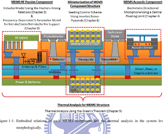
Figure 1-1: Embodied relations of each MEMS component and the thermal analysis in the system level morphologically ……… 5
Chapter 2
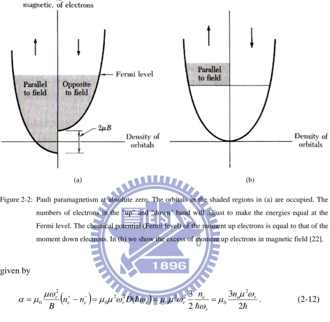
Figure 2-1: Real and imaginary parts of the susceptibility function in the neighborhood of two resonances. The region of anomalous dispersion is also the frequency interval where absorption occurs [27] ……… 14 Figure 2-2: Pauli paramagnetism at absolute zero. The orbitals in the shaded regions in (a)
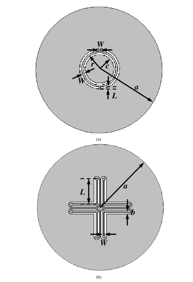
are occupied. The numbers of electrons in the "up" and "down" band will adjust to make the energies equal at the Fermi level. The chemical potential (Fermi level) of the moment up electrons is equal to that of the moment down electrons. In (b) we show the excess of moment up electrons in magnetic field [22] ……… 17 Figure 2-3: Schematic diagram of the two-port spiral polygon inductor realizations: (a)
rectangular, (b) octagonal, (c) circular spiral inductor. The parameters lmax, s,
and ϖ are the maximum edge, line spacing, and line width of the polygon
inductor, respectively ……… 18
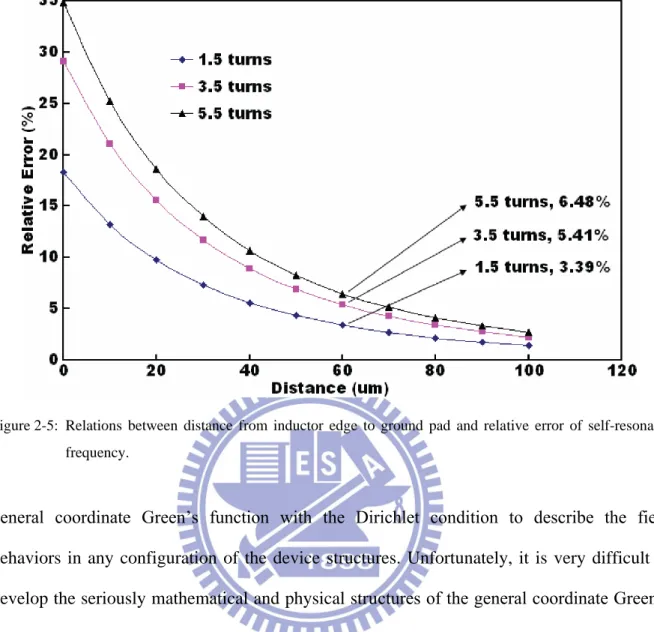
Figure 2-4: Band structure of the electron energy in a periodic lattice [26] ……… 20 Figure 2-5: Relations between distance from inductor edge to ground pad and relative error
of self-resonant frequency ……… 27 Figure 2-6: Scheme of a circular-like freely suspended spiral inductor under a removed
silicon substrate, at which a cylindrical cavity with radius of a and height d
was formed ……… 30
Figure 2-7: Scheme of a freely suspend micromachined rectangular spiral inductor with silicon substrate underneath removed and restricting its geometric factors as
lmax = 300 μm, S = 5 μm, and ϖ = 15 μm [34] ……… 32
Figure 2-8: Scheme of rectangular spiral inductor with substrate removed ………… 33 Figure 2-9: Scheme of octagonal spiral inductor with substrate removed ……… 34 Figure 2-10: Scheme of circular spiral inductor with substrate removed ……… 34 Figure 2-11: Smith chart in which a good s-parameter match between measurement and
simulation is present [4] ……… 36 Figure 2-12: Comparison of inductance spectrum of rectangular spiral inductors and results
of simulation ……… 37 Figure 2-13: Comparison of inductance spectrum of octagonal spiral inductors and results of
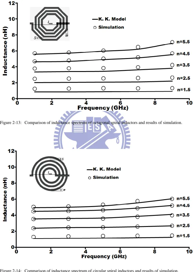
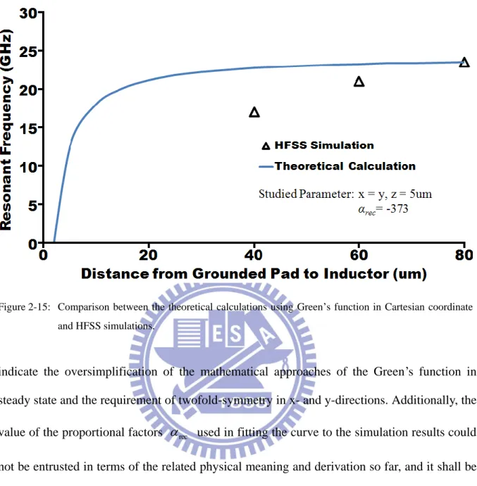
simulation ……… 38 Figure 2-14: Comparison of inductance spectrum of circular spiral inductors and results of
simulation ……… 38
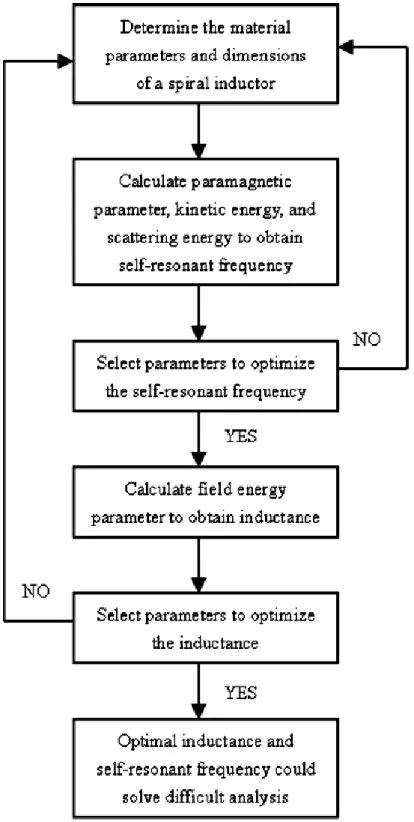
Figure 2-15: Comparison between the theoretical calculations using Green’s function in Cartesian coordinate and HFSS simulations ……… 39 Figure 2-16: A flow chart presents the step to optimize the inductor model ……… 43
Chapter 3
Figure 3-1: Comparison of experimental results between the losses of CPWs fabricated with and without oxide/nitride fin support on a conventional silicon substrate. The dimensions of CPW: 60μm strip width, 5μm thick, 150μm long and 12μm slot width. Both structures have the same dimensions ……… 48 Figure 3-2: Fabrication process flow: (a) Deep silicon trench etching, (b) thermal oxide
growth and top oxide removal, (c) ICP resident silicon etching, (d) LPCVD nitride deposition, and (e) CPW electroplating [49] ……… 49 Figure 3-3: A SEM cross sectional view on the CPW deposited on the patterned
nitride/oxide/nitride/air fins [49] ……… 49 Figure 3-4: A SEM cross sectional view of the as-fabricated oxide-nitride islands and an
enlarge view of Cu CPW fabricated on the top of oxide-nitride islands [49] ……… 50 Figure 3-5: The entire spectrums of phase shift of modeling data, simulated data, and
measured data with conventional and fin structure, respectively ……… 54 Figure 3-6: Comparison of HFSS simulation, model analysis, and experimental results of a
150μm long CPW on the silicon substrate with patterned oxide-nitride fins support ……… 55 Figure 3-7: Comparison of simulation results between the substrate loss of a spiral
inductor deposited on nitride/oxide/nitride/air fins and that on conventional silicon based substrate, respectively [49] ……… 56
Chapter 4
Figure 4-1: Schemes of central-supported gimbal circular biomimetic diaphragm. The upper insertion shows the auditory organ of the parasitoid fly Ormia ochracea whose entire auditory organ is only 1.2 mm. The intertympanal bridge
connecting two prosternal tympanal membranes (PTMs), i.e., the ipsilateral and the contralateral prosternal tympanal membranes, via the tympanal pits (TP) in a manner of flexible coupled pivot can cause the two PTMs to deflect in opposite directions. The lower insertion shows the mechanical model of the central-supported gimbal circular biomimetic diaphragm [57-66]
……… 59
Figure 4-2: Schematic diagrams regarding the geometrical structures for (a) the
conventional and (b) the hybrid C-S designs ……… 65 Figure 4-3: Scheme of the hybrid biomimetic microphone with central floating gimbal
design, which is hybridized by the acoustic sensing mechanism of the parasitoid fly and the flexible clover-stem-like gimbal structure. The lower insertion shows a new mechanical model with the central floating joint ……… 67 Figure 4-4: Comparison between the cloverleaf and the prototype of the biomimetic
microphone ……… 68
Figure 4-5: Examples of sinusoidal driven oscillatory motion with damping. The particular solution (steady-state) ZP(t), the complementary function ZC(t), and the
general solution of either ipsi- or contralateral displacement are shown in (a) driving frequency (ω) < damping frequency (ω′) and (b) driving frequency >
damping frequency, respectively [77] ……… 72 Figure 4-6: (a) A photograph of fabricated diaphragm embedded in a cylindrical cavity. (b)
A side view of the diaphragm [68] ……… 77 Figure 4-7: The comparison of the ipsilateral displacements of the conventional
biomimetic microphone between the theoretical calculations with varying damping rations and the measured data [68]. The damping ratios closed to unity indicates that the biomimetic microphone is critically damped so that the responses will directly follow the transient inputs ……… 78 Figure 4-8: Mechanical schemes and associated simulation results of deformation of the
conventional and hybrid C-S designs due to the influences of gravitational force. The conventional C-S design of the Case B only has two outer beams to support the entire mass of the diaphragm, whereas the hybrid one of the Case
C has four central beams to execute the same function ……… 80
Figure 4-9: Mechanical schemes and associated simulation results of deformation of the conventional and hybrid C-S designs due to the influences of sound source pressure. The hybrid C-S design of the Case D reveals larger displacements than that of the conventional one of the Case B, in which they have the same initial deformations ……… 81 Figure 4-10: Comparison of the (a) ipsilateral, (b) contralateral, and (c) net displacements
between model analyses and experimental measurement demonstrated by Ono
et al. [68] with applying 60 dB and 200 Hz sinusoid sound waves, respectively
……… 82 Figure 4-11: (a) The scheme and (b) the entire acoustic sensing system of Yu’s structurally
coupled design [82] ……… 83 Figure 4-12: The schematic process of the evolution from Yu’s design to the presented
Figure 4-13: Process flow of Fabrication ……… 86 Figure 4-14: SEM photograph of the hybrid microphone [84] ……… 87 Figure 4-15: Comparison of (a) the frequency spectra and (b) the logarithmic polar patterns
of net diaphragm displacement between hybrid and conventional C-S design [84] ……… 89 Figure 4-16: Acoustic responses of hybrid design in frequency domain in terms of (a)
amplitude, and (b) phase of ipsilateral and contralateral of diaphragm,
respectively [84] ……… 90
Figure 4-17: Measured (a) ipsilateral and (b) contralateral results of hybrid and CP-S design, respectively. Comparison of model and net displacement are of (c) CP-S and (d)
hybrid design, respectively ……… 90
Chapter 5
Figure 5-1: Scheme of the general electrothermal network π-model for thermal
management [91]. By analogizing with the common electric circuit π-model, there are three main blocks, heating source, propagated resistance, and common base resistance, are adopted to present the thermal source, thermal flow path, and the common base, respectively ……… 97 Figure 5-2: (a) Scheme of the 3-D stacked Vertical-Cavity Surface-Emitting Lasers
(VCSELs) on a Silicon Optical Bench (SiOB). It is obviously that there should be complicated thermal behavior inside the SiOB due to its large volume and aspect ratio. The insertion of upper-right corner shows complicated structure of the VCSELs, the adjacent contact pads, and the thermal via in detail. The insertion of upper-left corner shows the bottom structure of the VCSELs and the interconnected thermal conducting channels. The detail profiles of the (b) 45° micro-reflector and the (c) V-groove array that are monolithically
fabricated on the SiOB ……… 99 Figure 5-3: A cross-section of BeamExpress’s long-wavelength VCSEL [95] ……… 101 Figure 5-4: (a) Scheme of the modified general electrothermal network π-model. The
source of thermal flow and Z1 are the components of the heating source due to
the VCSELs are main heating generators themselves in our case. (b)The equivalent electrothermal circuit model of the VCSELs on the SiOB, where Z1
and Z2, Z3, and Z4 are thermal resistances of VCSEL (RVCSEL and R′VCSEL),
an infinite thermal resistance due to without nature air convection here, and the thermal capacitance of SiOB (CSiOB), respectively ……… 103
Figure 5-5: Scheme of conduction heat transfer sphere with specified volume and surrounding surface. The parameters qV and qS are the volume power density
in W/m3 generated within the interesting volume and surface power density in W/m2 radiated from the surrounding surface, respectively. The propagation direction of the surface power density is outward and parallel with the normal unit vector. The difference of the temperature distribution could be well determined using the derived conduction heat transfer equation in integral form ……… 107 Figure 5-6: Scheme of convection heat transfer sphere with specified surrounding surface.
The propagation direction of the surface power density is outward and
anti-parallel with the normal unit vector, nˆ. The difference of the temperature distribution could be well determined using the derived convection heat
transfer equation in integral form ……… 109 Figure 5-7: Transit isothermal maps of (a) the simulation results and (b) the EETCM-based
algorithm. Time interval between each map is about 30 ms and is evaluated by taking the trick that total input power within a mesh volume-element in a step of iteration divided by the power generated during 1 sec. ……… 112
Figure 5-8: Temperature distribution of single VCSEL realized using the presented
algorithm in steady state. The bottom of SiOB is constrained at 75°C to imitate the operation environment of a typical optical transceiver system ……… 115 Figure 5-9: Thermal images of the optical system heated by two operated VCSELs coding
by the presented algorithm ……… 115 Figure 5-10: The isothermal surfaces determined by means of the conduction and
convection heat transfer equation. In the case, only the lateral single laser turned on where represented using the symbol “+”. The input current is limited at 8 mA and the electric-thermal energy transfer efficiency is 85.7% to meet the standard specification of the semiconductor-made VCSELs [108]. The theoretical temperature at the hottest spot is 78.4°C ……… 117 Figure 5-11: (a) Scheme of the simplified thermal conducting system with single operating
VCSEL established by the EETCM. (b) The simulation result of simplified thermal conducting system. According the associated EETCM, the material of air and SiOB were removed in the system to reduce the required meshes as well as the CPU time and computer memory. The temperatures of node points A, B, and C are 78.9, 76.8, and 75°C while the input current is limited at 8 mA ……… 119 Figure 5-12: (a) Fabrication of SiOB and (b) Fabrication of High Frequency 4 Channel ×2.5
GHz Transmission Lines [94] ……… 121 Figure 5-13: The measured temperature distribution of SiOB heated by the operating
VCSEL using IR microscope. Only a laser diode is operated by probe B with 8 mA input current and 2 V bias voltage ……… 123 Figure 5-14: Comparison between the EETCM with single laser turned on, measurement
data, and simulated results with and without air and SiOB, respectively
Figure 5-15: The measured temperature distribution of SiOB heated by the operating VCSELs using IR microscope. Two laser diodes are operated with 8 mA input current and 2 V bias voltage ……… 124 Figure 5-16: Comparison between the EETCM with two lasers turned on, measurement data,
and simulated result, respectively ……… 125 Figure 5-17: Scheme of Successive Over-Relaxation (SOR) with (a) red- and (b) black
ordering [109]. During the first pass, the red nodes obtain the voltages as a weighted average of their original voltage, and as inputs (if any) to the six surrounding black nodes for 3D-situation. During the second pass, the black nodes obtain voltages from the six surrounding red nodes ……… 127 Figure 5-18: Scheme of the method for conceptually determining the temperature
distribution within each volume element of the situation that (a) single, and (b) two VCSELs are turned on. Each volume enclosed by the dash-line is an “isothermal volume.” The final given temperatures on the boundary surfaces, the temperature on the bottom, could determine the really temperature within the volume elements which are sharing the given temperatures on the boundary surfaces ……… 128 Figure 5-19: Scheme of the method for conceptually determining the probable path of heat
flux. Four current sources enclosed by four isothermal surfaces with the same temperature difference result in a fourfold overlapped region, the hottest region in this microsystem. Any of three or two current sources also result in the three- and twofold overlapped region and cause the temperature gradients within the system. Thus, the probable path of the heat flux would follow the ideal path that has the largest temperature gradient as indicated in the figure ……… 130
Chapter 6
Figure 6-1: Relations between the nominal radius, the temperature-dependent surface tension (a), and the inclined angle (b) ……… 137 Figure 6-2: The schemes of 1-D materials synthesis: (a) without and (b) with inclined
surface of inverted pyramid on silicon substrate ……… 138 Figure 6-3: SEM micrographs of a 6nm thick Co film on a silicon (100) substrate after (a)
800°C and (b) 900°C thermal reflow for 10 minutes, respectively [132,133] ……… 140 Figure 6-4: The bottom length of inverted pyramid versus the size of agglomerated Co
seed formed inside: (a) 6nm thick Co film deposition and (b) 30nm thick Co film deposition. Both substrates are thermally annealed at 900°C for 10 minutes [132,133] ……… 142 Figure 6-5: Auger line scanning spectrum across the region shown in the inset. The inset is
an enlarged SEM view on an inverted pyramid with the bottom length of 290nm inside which a singular Co seed is formed with the size of 190nm in diameter [132,133] ……… 144 Figure 6-6: (a) Array of the singular CNT. (b) SEM micrograph of a singular CNT grown
from a Co seed formed by the proposed seeding scheme which is reflowed with a 6nm Co seed layer. The insetted Raman spectra both in (a) and (b) indicate the CNTs are a multi-walled carbon nanotubes [133] ……… 145 Figure 6-7: The corresponding measured F-N plot for CNTs [129] ……… 152 Figure 6-8: Enhancement factor vs. the tube height for CNTs whose intertube distances are
(a) 104 and (b) 65 nm [133] ……… 152
Chapter 7
Chapter 1
Introduction
1.1 Overview
Since the concept of “infinitesimal machinery” was first proposed in 1959 by Dr. R. P. Feynman, the famous America physicist and the owner of Nobel Prize in physics, at the annual meeting of the American Physical Society at the California Institute of Technology (Caltech) [1-2], studies and techniques in the field of micro-electro-mechanical system (MEMS) regarding the integration of electrical and mechanical engineering, miniaturization, integrative fabrication method, diverse industrial and consumer applications then had been catching lots attention from the scientists and engineers. Due to the interdisciplinary MEMS technologies can inherit the advantages from solid-state material, microfabrication, and facility infrastructure, it can provide rapid pace of innovation and vast opportunities of ingenuity for a variety of applications ranging from electric, chemical, and mechanical engineering, material science, micro- and nanofabrication, life science, to civil and environment engineering, and so on.
A successful MEMS device cannot be developed without considering the varying technique connection and combination between science and engineering, thus a designer scientist or engineer who devotes in the field of MEMS would face with the inevitable challenges: the interdisciplinary design. For instance, a well-training electrical engineering designer who is developing a radio frequency (RF) antenna also might need to know the magnetic characteristics of a nanocomposite material to further enhance the performances of its passive components. A mechanical engineering designer should also have to search the fundamental knowledge about the solid state physics and corresponding fabrication skill to promote the performances of his devices efficiently. Thus, being involved in the diverse application domain, such as bioengineering, lab-on-a-chip, thermal phenomena, acoustic vibration, chemistry, nanotechnology, optical engineering, power and energy, hydrodynamics,
and wireless communication, the MEMS designers and engineers should create the desired impact with continuously developing their insight by grasping the essence in interdisciplinary design of knowledge [3]. In order to realize the connection between interdisciplinary applications, the interdisciplinary problems and challenges should be undertaken by the MEMS practitioners. In order to resolve the challenges, the physical models of every MEMS device eventually must be embedded in the technology of electronic design automation (EDA). System designers can, therefore, build their microsystem pre-designs according to the developed physical models use the hardware description language (HDL) in the EDA software platform, and then sequentially execute systematical simplification, simulations and performance predictions, systematical optimization, and layout, until achieve the goal of microsystem optimization. Thus, the EDA technique associate with the developed physical models could conveniently and conceptually provide the MEMS designers a whole picture of the microsystem design by considering the behavior dynamics of each adopted MEMS component and their cooperation, and enhance the efficiency and feasibility of the manufacture of MEMS products. Thus, in the dissertation, several MEMS component structures designed for different application have been fully analyzed for optimal microsystem designs. Five important MEMS component structures regarding a RF passive component characterized by the Kramer-Kronig relations [4,5], periodic fin support for reducing substrate loss [6], acoustic device with a specific central floating joint for sound source localization [7], 1D material for miniaturizing 3DIC applications [8], and SiOB thermal analysis using a special algorithm in view of integral form in system level for high speed data communication are presented for MEMS and NEMS devices for next generation applications [9].
Recent advancement in the design of portable wireless communication systems has been pushed to wide bandwidth applications, in which the carrier frequencies of the systems must shift to 5~10-GHz range or even higher. Thus, the passive components, such as inductor, capacitor, and transmission line, have to be implemented in the front-end RF circuitry for
excellent signal integrity and low power consumption requirements. The on-chip micromachined spiral inductors are one of the candidates developed for the purpose. Furthermore, a closed-form inductor model adopted in the design stage would be convenient for RFIC designers to pre-design and optimize the RF passive micromacnined spiral inductors in views of materials, geometries, and specially the energy interaction within the structure. To realize the energy interchange between free electrons and external electromagnetic waves within a MEMS RF passive component, freely suspended micromachining polygonal spiral inductors are investigated in detail. The resonant absorption and anomalous dispersion occurring at the self-resonance are considered as energy interchange between magnetic and electric energies. Meanwhile, a periodic structure constructed by a series of nitride/oxide/nitride/air fin support on the conventional silicon substrate is also presented to reduce the energy loss at high frequency region and reinforce the rigidity of the freely suspended component for further optimizing the performances of the MEMS RF passive components in microsystem designs.
Sound source localization is a physiological ability of animals to process sensory information regarding the orientation and magnitude of sound pressure stimulation. The source localization is achieved for a large mammal, two auditory organs are acoustically isolated by its head to have a large interaural distance (ID), via the nteraural intensity difference (IID) and interaural time delay (ITD) sensed by two ears which are geometrically close but far away from the sound sources. In contrast, two auditory organs of small animals are quite close to each other, so there would be a problem for the auditory system to experience insignificant interaural differences resulted by the tiny ID, about two orders of magnitude smaller than that of large animals. Therefore, the methodology of sound source localization in the tiny auditory system could lead the way to develop the next generation acoustic sensing and tracking microsystems like hearing aids, robots, and bionic military devices. Therefore, a biomimetic directional microphone is designed to understand the
mechanical coupling between the external sound pressures, viscous air damping forces, and a specified support structure. The microphone analysis provides a mathematical approach for MEMS engineers to realize the design trade-off between the performance and miniaturization of MEMS device. Superior sensitivity and directivity can be simultaneously reached by employing a novel central-supported structure, a central floating joint. By adequately judging dimensions of central beams of the presented design, the rocking and translational modes of the will get closer to each other and then theoretically reveal better membrane displacements.
For the microsystem development, undesired non-uniformly thermal effects due to drastic increase of the power dissipation within intensively operating chipsets have become significant design problems in the 3D-Stacking Structure (3D-SS) design, such as 3DICs, Silicon Optical Bench (SiOB), and Through Silicon Vias (TSV) Interposer, and so on, and even restrained the design flexibility in terms of associated configurations of device packaging system and maximum power performance of integrated system circuits. Figure 1-1 reveals the embodied relations schematically to further illustrate the interconnections of each MEMS structure and the thermal analyses in the microsystem level. One of proposed efficient strategies to build high-performance 3D microprocessors is to introduce thermal vias through layers or dies at specific locations. However, how to effectively deploy the layers with different thermal conductivities and minimize the utilization problem of interconnect vias in the structure should be strictly considered in associated algorithms [10-12]. Additionally, thermal interface materials used in chip- and package-level for heat dissipation [10,13] will also result in inevitable 3D-SS layout complication in design stage and manufacture cost increase in mass production which should be still undertaken. Thus, to conquer the drawbacks, this dissertation will present a new technique of thermal analysis accomplished by a developed equivalent electrothermal circuit model (EETCM) and an associated mathematical algorithm in system level for next generation 3D microsystem design applications. Simplification of any 3D-SS and the corresponding thermal analysis can be efficiently and
exactly characterized.
At final, to definitely reveal the three generic and distinct merits for MEMS devices: miniaturization, microelectronics integration, and mass fabrication with precision so that the MEMS practitioners could well follow the Moore’s Law, relative methodologies for the MEMS devices and its associated implement microelectronic circuitry thus become a key point for next generation. This requirement also impacts the electromechanical devices, bio-devices, and specific microsystem, so that searches were investigated to explore the scaling effect beyond that of the traditional MEMS [14-15]. Those devices and systems are then called nano-electromechanical systems (NMES), and many of which are developed using nanostructure assembly, such as nanotubes [15-16] or nanofabricated elements [17]. In this dissertation, the miniaturization of the MEMS are realized by means of a concept of one-dimensional (1D) material, in which vertical well-aligned carbon nanotubes (CNTs) are
Figure 1-1: Embodied relations of each MEMS component and the thermal analysis in the system level morphologically.
employed for visually constructing a three-dimensional integral circuit (3DIC) systems. Using gravitational force to trigger the metal liquids on the surfaces of inverted silicon nano-pyramids on the substrate, size and location of each vertical-aligned CNT can be well-defined. Therefore, combining with the suitable properties for microelectronics integration and ingenious seeding control scheme for precisely mass fabrication, the presented 1D material method can definitely provide an opportunity for further miniaturizing the MEMS and microelectronic devices.
1.2 Organization of the Dissertation
In Chapter 2, a closed-form integral model is presented for the freely suspended micromachining polygonal spiral inductor. The Kramers–Kronig relations provide an elegant theory and the causality between the interchange of magnetic and electric energies to describe the electron behavior within a polygonal spiral inductor without having complicated geometric analysis. A hypothesis built using similar mathematical approaches of the model of Pauli spin paramagnetism determines the resonant factor that described the resonant absorption of external electromagnetic energy while self-resonance occurring in the spiral inductor. Simulation and measurement results validate that the model can provide satisfactory prediction to the self-resonant frequencies and frequency-dependent inductances of on-chip freely suspended polygonal spiral inductors. Meanwhile, in Chapter 3, a structure of patterned nitride/oxide/nitride/air composited-fins on a silicon substrate with a resistivity of 1 -cm is presented to effectively reduce the substrate loss. A frequency-dependent S-parameter analytical model is also developed to predict characteristics of the coplanar waveguide (CPW). Comparisons for performances of rectangular spiral inductors on the composited-fins and conventional silicon substrate, respectively, show the practicality of the composited-fins support. A physical analysis of biomimetic microphone designed with a central-supported
(C-S) diaphragm for the sound source localization is presented in Chapter 4. A clover-stem-like C-S design is then proposed and resulting in 47% improvement of net diaphragm displacement. A central floating joint is employed in the hybrid C-S design and then reveals better resistance for preventing the undesired deformation and superior sensing ability beyond the conventional C-S one. Thus, the new design can effectively not only compensate undesired deformation of sensing diaphragm due to gravity and residual stresses but also make the diaphragm more flexible for better sound pressure sensitivity.
In Chapter 5, a method combining a general electrothermal network π-model in system level and the associated mathematical technique, Green’s theorem, in terms of the adopted materials and system geometries is presented to build up an equivalent electrothermal circuit model (EETCM) for efficient thermal analysis and behavior prediction in a thermal system. Heat conduction and convection transfer equations in integral forms are derived using the theorem and successfully applied for the thermal analysis of a 3D optical stack, VCSELs on a SiOB. The complicated stacking structure in conventional simulators can be greatly simplified using the method by well predicting probable heat flow paths, and the simplification can eventually achieve the goal of CPU time-saving without having complex mesh studying or scaling. By comparing the data from the measurement, the finite element simulation, and the method calculation, it shows that excellent temperature matching within ~0.5°C and 90% CPU time-saving can be realized.
A seeding control scheme by utilizing gravitational force to form an agglomeration of melted Co seeds on a patterned inverted silicon nano-pyramid is then presented in Chapter 6. Nanometer sized melted Co seeds formed on a nonwettable inverted pyramid surface can roll along the inclination followed by aggregation to form a singular seed with the size depending on the edge length of pyramid and the thickness of as-deposited Co film inside the pyramid. The associated physical mechanism of rolling and upper and lower limits of the radius of the Co drop-like liquids on the inclination are also definitely clarified. The proposed scheme
allowing the formation of well-aligned catalytic seeds with manipulated size will promise the control growth of 1D material for practical integrated microelectronic device fabrication.
Eventually, the rest chapters summarize the developed physical analyses of the MEMS component structures and the system, and then reveal the corresponding methods for the optimal microsystem designs and the future works. It is our belief that these analyses can definitely benefit the future development of microsystem EDA.
Chapter 2
A Closed-Form Integral Model of Spiral Inductors Using the
Kramers-Kronig Relations
2.1 Introduction
Researches in integral passives for the replacement of the discrete ones have shown growing importance for realizing the next generation electronics industry. The requirement for integral passives emerges from the increasing consumer demands for product miniaturization and high performance. The required components must, therefore, be reliable and controlled easily and the microelectronic industry has to respond the demands immediately. The last two decades have seen the development of personal computers, such as telecommunication, electronic equipment, devices and consumer sectors, towards product miniaturization with increasing functionality. In order to achieve the goal of miniaturization, the physical behaviors and related performance of miniaturized passive components must be understood clearly before being real products. In addition, National Electronics Manufacturing Initiative (NEMI) has well defined the integral passive as the functional elements either embedded in or incorporated on the surface of an interconnecting substrate. Since the number and areas of passive components may exceed both that of IC chips on a circuit board or a package, it is necessary to concretely estimate and predict each single device’s performance and the interaction between each other. As a result, it is necessary to develop a method to well predict and then optimize the behaviors of the passive components accompanied with the benefits of smaller size, more functionality, and better performance.
The micromachined spiral inductors, one of the critical passive components, have been properly developed and widely utilized for RFIC designs. The related electric characteristics, including self- and mutual inductances, quality factors, self-resonant frequencies, and loss mechanism etc. of the inductor, have already been investigated in detail. A variety of methodologies to calculate the inductance of a spiral inductor, such as Greenhouse-based
formulations [18-20], empirical expressions [21], analysis and simulation of inductors and transformers in integrated circuits (ASITIC) [22], and several textbooks in physics and engineering, have been presented for the design principles.
Nevertheless, in order to facilitate the implementation of integrated inductors, a compact scalable physical model that can accurately predict the physical behaviors of the inductors in terms of material, geometrical, and overall configured parameters is still an important research topic for the RFIC design and optimization [21,23-27]. Conventional inductor models [21,24] could calculate inductance precisely. The applied method, however, is based on the Greenhouse algorithm [18], which has high accuracy but still relies on numerous summation steps that depend on the number of interacting segments and overall combinations of parallel segments so that a complicated geometrical analysis could not be avoided. Meanwhile, several aforementioned methods only can provide nonphysical expressions using a large number of fitting factors, the lack of sufficient physical and mathematical meanings of the presented models result in the difficulties of optimization in design stage. Since the factors are created to overcome the imperfect of the fitting function, it is also essential to create an accurate mathematical expression associated with the physical sense for predictions of the physical behaviors of a micromachined spiral inductor.
In this chapter, a closed-form integral model is presented for freely suspended micromachined polygonal spiral inductors. Based on the Kramers-Kronig relations, field theory, and solid state physics [26-28], the presented model can actually describe behaviors of free electrons in a metal to characterize physical parameters of a spiral inductor which RFIC designers could easily have the optimal design. Meanwhile, this model can exactly predict inductances and self-resonant frequencies of spiral inductors without complicated geometrical analysis. Simulation and measurement results have validated the accuracy of the model. Furthermore, unlike conventional formulations only based on circuit parameters, this model analysis provides physical intuition in terms of materials and geometry.
2.2 Linear Response Theory, Causality, and Kramers-Kronig Relations for Metals
An external filed applies on, or more strictly perturb, an interesting system, the physical characteristics of the system, such as thermal qualities or electron distribution, would provide corresponding responses. While the quantity of external field (or say, the perturbation) is sufficient weak, the response of the system is linearly proportional to the stimulus. The proportional factor is generally called a linear response function or a generalized susceptibility that can be expressed using the Green’s function. Meanwhile, two prescribed conditions should be achieved before obtaining the response function:
(1) The external field shall be so sufficient weak that the associated Hamiltonian of the system would become perturbed equations such as the generalized form of Hook’s law. Thus, the concerned physical problem would be reduced as a linear combination of linear response functions. For instance, by employing the Faltung theorem of Fourier integrals, the temporally nonlocal connection between the displacement field
) , ( tx
D and the electric field E( tx, ) can be expressed as [21]:
E x t G E x t d t x D( , ) 0 ( , ) ( ) ( , ) , (2-1)where G() is the Fourier transform of the electric susceptibility, e, (or the response function):
i d i d G e 1 exp( ) ) ( 2 1 ) exp( 2 1 ) ( 0 . (2-2)The parameters 0 and () are the permittivity constant in free space and the frequency-dependent dielectric constant, respectively. The response function in (2-1) clarifies the responses of the medium, in which an electric susceptibility would be induced due to the external electric field.
(2) The responses could directly follow with the stimulus, thus the system should be assumed in an adiabatic environment. The system is in equilibrium or at ground state when the propagated time is at the condition of t = 0. To judge whether our concerning problems in the RF regime could be reduced as a linear response functions or not, we can clearly consider and examine the frequency-dependent Ohmic law in view of solid state theory [26-29]:
) , ( ) ( ) , (x E x J , (2-3)
where the electric conductivity () is a complex physical parameter:
r r e r e i i m e n 1 1 1 ) ( 0 2 . (2-4)
The parameters n , e, e r, and me, are the density of free electron, the charge element,
the relaxation time, and the mass of a electron, respectively. Generally, for a simple metal such as copper, the relaxation time is typically 10-14 second [28,29]. Thus, within the RF even the terahertz radiation (TR) region, the condition r 102 1 results in the imaginary part could be safely ignored in (2-4). The consequence indicates that the current is definitely in-phase with the associated driving time-varying electric filed, and the energy of the electromagnetic field would be absorbed in form of Joule heat due to the finite resistance of the metal.
Therefore, as mentioned above, the physical behaviors and the corresponding responses due to the external frequency-dependent stimulus of the micromachined spiral inductor could be definitely clarified and analyzed based on the linear response theory. The rest problem is: can the linear response theory reveal the causality of the interaction between the stimulus and the responses in the interesting system, so that the quantitative relationships between attenuation and dispersion of the system could be uniquely determined? To overcome the risk, the
Kramers-Kronig relations are employed in this chapter. As a prescribed consequence, the Kramers-Kronig relations will be the core key to resolve the physical behaviors of the micromachined spiral inductor.
The Kramers-Kronig relations compose of one of the most elegant and general theorems in physics, because they depend only on the principle of causality for their validity: the response cannot be prior to the stimulation. Simply based on the principle, the Kramers-Kronig relations describe the interdependence of the real and imaginary parts of the generalized susceptibility χ
ω . Thus, the Kramers-Kronig relations can explain in the most fundamental and general terms, completely independent of the underlying physical mechanisms, the intimate connection between refraction and absorption. In fact, given one, the other follows immediately. To evaluate the behavior of low frequency due to the singularity for a conducting medium in the case (this can be realized that the condition1
r
is satisfied automatically), the generalized response functions derived by the Kramers-Kronig relations can be expressed as [26-30]:
0 2 0 2 0 )] ( Im[ 2 )] ( Re[ g P g d , (2-5) and
0 2 0 2 0 0 )] ( Re[ 2 )] ( Im[ g P g d , (2-6)where σ0 is the dc conductivity of metal as shown in (2-4), and the 0 is the eigen- frequency of the response functions. The detail mathematical derivation of the Kramers-Kronig relations could be found in the Reference [26-30]. Therefore, the Kramers-Kronig relations for metals are definitely presented.
2.3 Determination of the Self-Resonant Frequency of a Spiral Inductor
2.3.1 Characteristics of Anomalous Dispersion and Resonant Absorption
In this section, the concurrence relationships of the real and imaginary parts of the Kramers-Kronig relations are modified to explain certain physical characteristics. For instance, preceded with the Lorentz–Drude Model (1900) in a conducting medium, a phenomenon called anomalous dispersion occurring near a narrow absorption feature, i.e., resonant absorption in a metal vapor, can be well represented in terms of the utilization of equation (2-5) and (2-6) to describe the relation between resonant absorption and anomalous dispersion as shown in Figure 2-1. The dispersion and absorption are coupled with each other and associated with the real and imaginary parts of the susceptibility, respectively. If a medium has an imaginary component of the susceptibility at the self-resonant frequency, it must have a real component over a broad range of frequencies around the self-resonant frequency. While
Figure 2-1: Real and imaginary parts of the susceptibility function in the neighborhood of two resonances. The region of anomalous dispersion is also the frequency interval where absorption occurs [27].
the resonance occurs, the energy of incident electromagnetic waves are fully absorbed by the free electrons inside the medium and the frequency diagram of the absorption would be peaked strongly at the resonant frequency. Similar physical behavior of the resonance should be also applicable for the case of a micromachined spiral inductor. The self-resonance occurrence of the spiral inductor would result in a complete energy transformation from stored magnetic energy into electrical energy, and vice versa. The occurrence of the energy exchange is similar to the anomalous dispersion in which the incident electromagnetic waves are totally absorbed by the conducting medium and transformed into the kinetic energy and scattering potential of the free electrons. Therefore, we can construct a physical-based inductor model using the Kramers-Kronig relations based on the mentioned linear response theory and the causality of the responses. First, we assume that the inductor is perfect for electromagnetic wave signal propagation without having any energy loss except the Joule heating. Fortunately, the Joule heating should be smaller than the kinetic and potential energies, thus it can be safely ignored in the derivation. Thus, the imaginary part, (2-6), could be rationalized as a very narrow absorption of the electromagnetic wave at self-resonant frequency, ωr, due to the energy transformation and it can be modified as [27]:
... 2 Im r r d , (2-7)which is accompanied with the real part as the following:
2 2 Re r d d , (2-8)where d is the slow part of (2-8) resulted by the more remote contributions to (2-7). The resonant factor α can be evaluated by employing similar mathematical and physical approaches as the model of Pauli spin paramagnetism [28,29]. For discussion in high frequency region, the new response function can be then reduced as:
![Figure 2-4: Band structure of the electron energy in a periodic lattice [26].](https://thumb-ap.123doks.com/thumbv2/9libinfo/8741151.204234/45.892.276.669.117.471/figure-band-structure-electron-energy-periodic-lattice.webp)
![Figure 2-11: Smith chart in which a good s-parameter match between measurement and simulation is present [4]](https://thumb-ap.123doks.com/thumbv2/9libinfo/8741151.204234/61.892.196.758.509.1030/figure-smith-chart-parameter-match-measurement-simulation-present.webp)
![Figure 3-3: A SEM cross sectional view on the CPW deposited on the patterned nitride/oxide/nitride/air fins [49]](https://thumb-ap.123doks.com/thumbv2/9libinfo/8741151.204234/74.892.134.798.109.571/figure-cross-sectional-deposited-patterned-nitride-oxide-nitride.webp)