適用於3GPP之Radix-4渦輪碼解碼器
62
0
0
全文
(2) 適用於 3GPP 之 Radix-4 渦輪碼解碼器. A Radix-4 Turbo Decoder for 3GPP. 研 究 生:廖盈超. Student:Ying-Chao Liao. 指導教授:蔡尚澕. Advisor:Shang-Ho Tsai. 國 立 交 通 大 學 電 機 與 控 制 工 程 學 系 碩 士 論 文. A Thesis Submitted to Department of Electrical and Control Engineering College of Electrical Engineering and Computer Science National Chiao Tung University in Partial Fulfillment of the Requirements for the Degree of Master In Electrical and Control Engineering. December 2008 Hsinchu, Taiwan, Republic of China. 中華民國 九 十 七 年 十二 月.
(3) 適用於 3GPP 之 Radix-4 渦輪碼解碼器. 指導教授:蔡尚澕. 學生:廖盈超. 國立交通大學電機與控制工程學系﹙研究所﹚碩士班. 摘. 要. 渦輪碼已經廣範使用在通訊系統,因為它有極佳的錯誤修正能力。為了增加扇出數和減少所需 的記憶,開始研究渦輪碼 radix-4 架構。可是在 radix-4 的渦輪解碼器所需的計算路徑較長,使 得 radix-4 渦輪解碼器的扇出數無法高於 radix-2 渦輪解碼器 2 倍。在這篇論文中我們在遞迴架 構中提出一個查表方針,使得扇出數增加 62%,在提出的方法下效能僅比 Log-MAP 差 0.025dB。應用在超大型積體電路上,我們在輸入緩衝器使用 dual-RAM 取代成 single-RAM, 這樣可以減少面積 57.8%及減少功率 71.83%。晶片是採用 TSMC 0.18 μ m CMOS 製程,操作 頻率在 167MHz,電壓為 1.62 伏特。使用 3GPP 規格碼率為 1/3,扇出數為 22Mb/s 下,消耗功 率為 135mW,而晶片的面積為 2.65 mm2 包含 200K 的邏輯閘數。.
(4) A Radix-4 Turbo Decoder for 3GPP. Student:Ying-Chao Liao. Advisors:Dr. Shang-Ho Tsai. Department﹙Institute﹚of Electrical and Control Engineering National Chiao Tung University. ABSTRACT Turbo code has been widely used in communication systems, because of its outstanding error correction performance. To increase throughput and decrease the required memory. Radix-4 architecture for Turbo decoder was studied. However, the critical path of the recursive architecture in Radix-4 turbo decoder is long, As a result conventional Radix-4 architecture [15] cannot achieve twice throughput over the conventional Radix-2 architecture. In this thesis, we proposed a Look-Up Table scheme for the recursive architecture and the throughput increases up to 62%. The performance of the proposed scheme is worse than the Log-MAP (optimal) by only 0.025dB. In VLSI implementation, we propose a method for input buffer and it can reduce the dual-RAM by the single-RAM to save area and power. The proposed method can reduce the area by 57.8% and the power by 71.83%. The chip is fabricated in TSMC 0.18 μm CMOS process, operating at 167MHz clock rate with voltage supply 1.62V. The power consumption is 135mW at decoding rate 22Mb/s, with code rate 1/3 for 3GPP standard. The core area is 2.65 mm², contain 200K gate counts..
(5) 誌. 謝. 經過了兩年研究所的生涯終於告一段落了,此篇論文能夠順利的 完成非常感謝的是我的指導教授蔡尚澕教授,在兩年的研究生活中, 在研究上遭遇到很多困難,但老師很仔細的了解原因所在並一一地幫 忙解決,使得我可以繼續研究下去。並感謝我的口試委員:林源倍教 授、簡鳳村教授、董蘭榮教授提供我寶貴意見,以彌補論文不善之處。 另外,感謝陳宇文、葉柏賢同學,因為有你們的幫忙,讓我在研 究之路上得到幫忙和勉勵,使我獲益良多。也感謝學弟妹們的加入, 因為有你們的加入使我們研究室的氣氛更加和樂。 最後,我要感謝的是我的父母,因為有他們給我無後顧之憂才使 得研究可以完成,也因為有你們的支持與鼓勵讓我遇到困難都能迎刃 而解。.
(6) A Radix-4 Turbo Decoder for 3GPP. Ying-Chao Liao. Advisor: Dr. Shang-Ho Tsai Department of Electrical and Control Engineering National Chico Tung University December 4, 2008. Abstract Turbo code has been widely used in communication systems, because of its outstanding error correction performance. To increase throughput and decrease the required memory. Radix-4 architecture for Turbo decoder was studied. However, the critical path of the recursive architecture in Radix-4 turbo decoder is long, As a result conventional Radix-4 architecture [15] cannot achieve twice throughput over the conventional Radix-2 architecture. In this thesis, we proposed a Look-Up Table scheme for the recursive architecture and the throughput increases up to 62%. The performance of the proposed scheme is worse than the Log-MAP (optimal) by only 0.025dB. In VLSI implementation, we propose a method for input buffer and it can reduce the dual-RAM by the single-RAM to save area and power. The proposed method can reduce the area by 57.8% and the power by 71.83%. The chip is fabricated in TSMC 0.18 µm CMOS process, operating at 167MHz clock rate with voltage supply 1.62V. The power consumption is 135mW at decoding rate 22Mb/s, with code rate 1/3 for 3GPP standard. The core area is 2.65 mm2 , contain 200K gate counts..
(7) Contents 1 2. Introduction Turbo Code. 1. 2.1 Turbo Code Encoder . . . . . . . . . . . . . . . 2.1.1 Recursive Systematic Convolution Codes 2.1.2 Termination of encoding process . . . . . 2.2 Decoding Criterion . . . . . . . . . . . . . . . . 2.2.1 MAP criteria . . . . . . . . . . . . . . . 2.2.2 Log-MAP and Max-Log-MAP criteria . . 2.3 Decoding Algorithm . . . . . . . . . . . . . . . 2.3.1 Radix-2 algorithm . . . . . . . . . . . . 2.3.2 Radix-4 algorithm . . . . . . . . . . . . 2.3.3 Deriving LLR for Radix-4 . . . . . . . . 2.4 Decoding Architecture . . . . . . . . . . . . . . 2.4.1 Sliding Window . . . . . . . . . . . . . . 3. . . . . . . . . . . . .. . . . . . . . . . . . .. . . . . . . . . . . . .. . . . . . . . . . . . .. . . . . . . . . . . . .. . . . . . . . . . . . .. . . . . . . . . . . . .. . . . . . . . . . . . .. . . . . . . . . . . . .. Radix-4 Recursive Architecture . . . .. . . . .. . . . .. . . . .. . . . .. . . . .. . . . .. 21 21 21 26 28. 4.1 Hardware Design for 3GPP . . . . . . . . . . . . . . . 4.1.1 Input Bu¤er . . . . . . . . . . . . . . . . . . . . 4.1.2 BMU(branch metric unit ) . . . . . . . . . . . . 4.1.3 OACS(O¤set-Add-Compare-Select) . . . . . . . 4.1.4 LLR (Log-Likelihood Ratio ) . . . . . . . . . . 4.1.5 Extrinsic Information and a Priori Information . 4.1.6 Interleaver and De-interleaver . . . . . . . . . . 4.1.7 Hard Decision . . . . . . . . . . . . . . . . . . . 4.1.8 Sliding Window . . . . . . . . . . . . . . . . . .. . . . . . . . . .. . . . . . . . . .. . . . . . . . . .. . . . . . . . . .. . . . . . . . . .. . . . . . . . . .. 30 30 30 34 36 36 37 39 39 40. 3.1 Conventional Architecture . . . 3.2 Proposed Architecture . . . . . 3.2.1 Performance Comparison 3.3 Fixed point Analysis . . . . . . 4. . . . . . . . . . . . .. 3 3 3 4 5 5 7 11 11 12 14 17 20. . . . .. . . . .. . . . .. . . . .. . . . .. . . . .. . . . .. . . . .. . . . .. . . . .. . . . .. . . . .. VLSI Implementation. i.
(8) 4.2 Design ‡ow . . . . . . . . . . 4.2.1 System model . . . . . 4.2.2 RTL code . . . . . . . 4.2.3 BIST . . . . . . . . . . 4.2.4 Synthesis . . . . . . . 4.2.5 Gate-level simulation . 4.2.6 DFT . . . . . . . . . . 4.2.7 ATPG . . . . . . . . . 4.2.8 APR . . . . . . . . . . 4.2.9 DRC and LVS . . . . . 4.2.10 Post-layout level . . . 4.3 Chip Layout and Comparison 5. . . . . . . . . . . . .. Conclusion. . . . . . . . . . . . .. . . . . . . . . . . . .. . . . . . . . . . . . .. . . . . . . . . . . . .. . . . . . . . . . . . .. . . . . . . . . . . . .. . . . . . . . . . . . .. . . . . . . . . . . . .. . . . . . . . . . . . .. . . . . . . . . . . . .. . . . . . . . . . . . .. . . . . . . . . . . . .. . . . . . . . . . . . .. . . . . . . . . . . . .. . . . . . . . . . . . .. . . . . . . . . . . . .. . . . . . . . . . . . .. . . . . . . . . . . . .. . . . . . . . . . . . .. 41 41 44 44 44 44 45 45 45 45 46 47 49. ii.
(9) List of Figures 2.1 2.2 2.3 2.4 2.5 2.6 2.7. The Turbo Code Encoder for 3GPP. . . . . . . . . . . . . . . . . A general form of max ( ): . . . . . . . . . . . . . . . . . . . . . . The trellis diagram of : . . . . . . . . . . . . . . . . . . . . . . . The trellis diagram of : . . . . . . . . . . . . . . . . . . . . . . . The Radix-2 and Radix-4 trellis diagram. . . . . . . . . . . . . . . The trellis diagram of LLR unit for stage t : (a) LLRt1 and (b) LLRt0 : 1 The trellis diagram of LLR unit for stage t + 1 : (a) LLRt+1 and 0 (b) LLRt+1 . . . . . . . . . . . . . . . . . . . . . . . . . . . . . . . 2.8 An architecture of the turbo decoder. . . . . . . . . . . . . . . . . 2.9 The sliding window diagram. . . . . . . . . . . . . . . . . . . . . .. 4 9 12 13 15 18. 3.1 3.2 3.3 3.4 3.5. Conventional Radix-4 Architecture. . . . . . . . . . . . . . . . . . Radix-4 recursion architecture of [20] . . . . . . . . . . . . . . . . Architecture of the proposed LUT used in [20]. . . . . . . . . . . . Architecture of the proposed LUT. . . . . . . . . . . . . . . . . . Performance comparison among the Log-MAP and four approximated algorithms. . . . . . . . . . . . . . . . . . . . . . . . . . . .. 22 23 24 25. 4.1 The turbo decoder architecture with a single SISO decoder. . . . . 4.2 The input data ‡ow. . . . . . . . . . . . . . . . . . . . . . . . . . 4.3 The proposed ROM and RAM scheme to achieve two-read and two-write in one clock cycle. . . . . . . . . . . . . . . . . . . . . . 4.4 Timing diagram for the proposed RAM and ROM schemes. . . . . 4.5 The architecture of : . . . . . . . . . . . . . . . . . . . . . . . . . 4.6 The normalization of OACS. . . . . . . . . . . . . . . . . . . . . . 4.7 The Architecture of LLR. . . . . . . . . . . . . . . . . . . . . . . 4.8 The hardware architecture of max ( ): . . . . . . . . . . . . . . . 4.9 Timing diagram of a priori information for two Dual-RAMs. . . . 4.10 The architecture of hard decision. . . . . . . . . . . . . . . . . . . 4.11 Calculating BMU, OACS and LLR. . . . . . . . . . . . . . . . . . 4.12 Timing diagram of Sliding Window. . . . . . . . . . . . . . . . . . 4.13 IC design ‡ow. . . . . . . . . . . . . . . . . . . . . . . . . . . . . 4.14 Chip layout of the proposed Radix-4 Turbo Decoder for 3GPP. . .. 31 33. iii. 18 19 20. 29. 34 35 36 37 38 38 39 40 41 42 43 47.
(10) List of Tables 3.1 3.2 3.3 3.4. Approximation of [20]. . . . . . . . . . . . . . . . . . The values of g(x); u(v); d1 ; d0 and p1 ; p0 . . . . . . . Comparison of various recursive architectures. . . . . Quantization format for the proposed Turbo Decoder.. . . . .. 24 27 28 28. 4.1 Summary of interleaver process with four case. . . . . . . . . . . . 4.2 Comparision of area and power for implementing the input bu¤er by dual-RAM and singl-RAM. . . . . . . . . . . . . . . . . . . . . 4.3 The expected turbo decoder chip summary. . . . . . . . . . . . . . 4.4 Chip comparison. . . . . . . . . . . . . . . . . . . . . . . . . . . .. 32. iv. . . . .. . . . .. . . . .. . . . .. . . . .. . . . .. 33 48 48.
(11) Chapter 1 Introduction The basic concept of channel coding is to add redundance bits along with information bits before transmission. These redundance bits can help the receiver to decode data correctly with higher probability. In 1984, Shannon proposed a limit on the maximum achievable data rate over a channel. Many researchers attempt various methods to close the Shannon limit. In 1993, Turbo Code was proposed by Berrou, Glavieux and Thimajashima [1], it is a powerful error correcting codes whose performance is close to shannon limit. In many mobile communication systems, turbo code has been adopted to gain better performance, such as in WCDMA, CDMA2000 [2], WiMAX and 3G [3] standards. The turbo encode consists of two Recursive Systematic Convolutional (RSC) encoders [18] and one interleaver. For the turbo decoder, it consists of two soft-input soft-output (SISO) decoders and one interleaver/deinterleaver between them. The SISO decoder is used in turbo decoder. In addition, it is also applied in some other algorithm such as SOVA (Soft Out Viterbi Algorithm) [4]-[6], LogMAP, Max-Log-MAP [7] and improved Max-Log-MAP [8] (approximations to the MAP algorithm). Interleaver design for 3GPP was proposed by [10]-[12], to support full block length. In 2003, Lucent Bell Labs [15] proposed the radix-4 algorithm for turbo decoder. The algorithm has two advantages. One is doubling the throughput for a given clock rate over the radix-2 architecture, and the other is reducing the memory. Hence, in recent years, radix-4 turbo code is studied, e.g. see [20], [21]. 1.
(12) which proposed methods to improve the recursive architecture for radix-4 turbo code decoder. As for VLSI implementation for turbo decoders, the sliding window algorithm ([16], [17]) is proposed to avoid storing the metrics corresponding to the entire codeword sequence to reduce the memory requirement. In this thesis, we use Radix-4 algorithm, approximated Log-MAP [20] and sliding window technique to implement turbo decoder for 3GPP standard. Moreover, we proposed a Look-Up Table scheme for the recursive architecture and the throughput increases up to 62% over the traditional Radix2 algorithm. In VLSI implementation, we propose a method for input bu¤er and it can reduce the dual-RAM by the single-RAM to save area and power. The proposed method can reduce the area by 57.8% and the power by 71.83%. The chip is fabricated in TSMC 0.18 m CMOS process. The expected clock rate is 167MHz, throughput is 22Mb/s, and the power consumption is 135mW with code rate 1/3, block length 512. The core area is 2.65 mm2 , containing 200K gate counts. The chapters are organized as follows. In Chapter 2, we describe the MAP criteria, Log-MAP criteria and Max-Log-MAP criteria. Also we compare decoding algorithm for radix-2 and radix-4. Operation of sliding window technique is also described here. In Chapter 3 we introduce the proposed scheme for radix-4 recursive architecture, and compare it to various recursive architectures. Chapter 4 introduces the VLSI implementation, we describe how to use one single RAM to achieve Dual-RAM operation for Radix-4 turbo decoder. Also we describe the decoding ‡ow with hardware architecture and show the chip layout as well as the corresponding chip performance comparison.. 2.
(13) Chapter 2 Turbo Code In 1993, The turbo code was introduced by Berrou, Glavieux, and Thitimajshima [1], and achieved a bit-error probability of 10. 5. with a code rate of 1/2. over an AWGN (additive white Gaussian noise) channel and BPSK modulation at an Eb =N0 of 0.7dB. Turbo code has been adopted in many mobile communication systems, such as WCDMA, CDMA2000, WiMAX, 3G mobile. In 3GPP [3] systems, the turbo encoder consists of two Recursive Systematic Convolutional (RSC) [18] codes in parallel and an interleaver unit. For turbo decoder, it consists of two Maximum A Posteriori (MAP) decoders connected in series with a feedback loop from the second output to the …rst input. Let us introduce the codec more detailed in the following subsections.. 2.1 2.1.1. Turbo Code Encoder Recursive Systematic Convolution Codes. Fig. 2.1 is the turbo code encoder structure in 3GPP systems and code rate is 1/3. The encoder consists of two RSC codes and an interleaver. The generator matrix of the RSC encode is: g1 (D) , g0 (D). (2.1). g0 (D) = 1 + D2 + D3. (2.2). G(D) = 1; where. 3.
(14) xk. 1st RSC Encoder. ck A. D. D. zk. D. B. 2nd RSC Encoder. interleaver. c′k. A′. D. D. z ′k. D. B′. xk′ Figure 2.1: The Turbo Code Encoder for 3GPP.. is the feedback polynomial and g1 (D) = 1 + D + D3. (2.3). is the forward polynomial. Initially, the registers from RSC must be zero ,and upper switch and lower switch switch to A and A. After K numbers are inputted, thus the order of the output from the turbo encoder is x1 ; z1 ; z1 ; x2 ; z2 ; z2 ;...; xK ; zK ; zK where x1 ; x2 ;...; xK are input bits and K is the number of input bits.. 2.1.2. Termination of encoding process. The termination scheme is to let the encoder comes back to zero state and thus it can decrease the bit error rate. When the K bits completes encoding process, both the two RSCs need to generate 12 tail bits. First, the lower RSC in Fig. 2.1 is disable and the switch in the upper RSC is changed from position A to position B, and then six tail bits are generated. Second, the last six tail bits are generated by turning o¤ the upper RSC and the switch in the lower RSC is. 4.
(15) changed from position A to position B. The 12 tail bits shall be: xK+1 , zK+1 , xK+2 , zK+2 , xK+3 , zK+3 , xK+1 , z K+1 , xK+2 , z K+2 , xK+3 , z K+3 : (2.4). 2.2 2.2.1. Decoding Criterion MAP criteria. The MAP algorithm has been developed by Bahl, Cocke, Jelinek, and Raviv in 1974 [13] and is termed as BCJR algorithm. Consider a situation that we received a signal r over a discrete memoryless channel. The state transitions from state m to state m, i.e. Sm (t) at time t to Sm (t + 1) at time t + 1, we can obtain a joint probability: PrfSm (t); Sm (t + 1); rg. (2.5). N 1 = PrfSm (t); Sm (t + 1); r0t 1 ; rtt ; rt+1 g:. Using joint probability property Pr(A; B) = Pr(A) Pr(BjA). (2.6). Pr(A; B) = Pr(B) Pr(AjB),. (2.7). or. we can rewrite (2.5) as follows (2.8). PrfSm (t); Sm (t + 1); rg N 1 = PrfSm (t); Sm (t + 1); r0t 1 ; rtt g Prfrt+1 jSm (t); Sm (t + 1); r0t 1 ; rtt ). N 1 = PrfSm (t); r0t 1 g PrfSm (t + 1); rtt jSm (t); r0t 1 g Prfrt+1 jSm (t); Sm (t + 1); r0t 1 ; rtt g N 1 = PrfSm (t); r0t 1 g PrfSm (t + 1); rtt jSm (t)g Prfrt+1 jSm (t + 1)g,. where rab ; means that receive signals from time instance a to time instance b. From (2.8), let us de…ne three functions for description convenience, i.e. (Sm (t)) = PrfSm (t); r0t 1 g; N 1 (Sm (t + 1)) = Prfrt+1 jSm (t + 1)g;. 5. (2.9) (2.10).
(16) and (Sm (t); Sm (t + 1)) = PrfSm (t + 1); rt jSm (t)g:. (2.11). Hence (2.8) can be rewritten as: PrfSm (t); Sm (t + 1); rg = (Sm (t)) (Sm (t); Sm (t + 1)) (Sm (t + 1)):. (2.12). De…ne S be the set of all the states at time t. We can further extend (2.9) as (Sm (t + 1)) = PrfSm (t + 1); r0t g X = PrfSm (t); Sm (t + 1); r0t g Sm (t)2S. X. =. Sm (t)2S. X. =. Sm (t)2S. X. =. PrfSm (t); r0t 1 g PrfSm (t + 1); rt jSm (t); r0t 1 g PrfSm (t); r0t 1 g PrfSm (t + 1); rt jSm (t)g (Sm (t)) (Sm (t); Sm (t + 1)):. (2.13). Sm (t)2S. Similarly, de…ne S be the set of all the states at time t + 1. We can further extend (2.10) as (Sm (t)) = PrfrtN X =. 1. jSm (t)g PrfSm (t + 1); rtN. Sm (t+1)2S. =. X. Sm (t+1)2S. =. X. Sm (t+1)2S. =. X. 1. jSm (t)g. N 1 Prfrt+1 jSm (t + 1); rt ; Sm (t)g PrfSm (t + 1); rt jSm (t)g N 1 Prfrt+1 jSm (t + 1); rt g PrfSm (t + 1); rt jSm (t)g. (Sm (t + 1)) (Sm (t); Sm (t + 1)):. (2.14). Sm (t+1)2S. Finally, the branch metric can be rewritten as (Sm (t); Sm (t + 1)) = PrfSm (t + 1); rt jSm (t)g: From the Bayes’rule Pr(AjB) = 6. Pr(A; B) , Pr(B). (2.15).
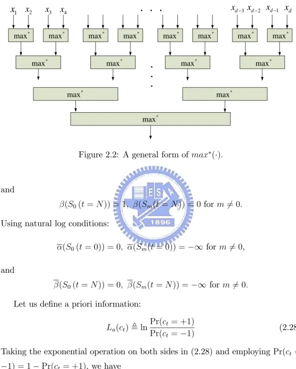
(17) we can rewrite (2.15) as PrfSm (t + 1); Sm (t); rt g PrfSm (t)g PrfSm (t + 1); Sm (t)g PrfSm (t + 1); Sm (t); rt g = PrfSm (t)g PrfSm (t + 1); Sm (t)g = PrfSm (t + 1)jSm (t)g Prfrt jSm (t + 1); Sm (t)g. (Sm (t); Sm (t + 1)) =. = Pr(ct ) Pr(rt jwt ),. (2.16). where ct is encoder input that make the state change from Sm (t) to Sm (t + 1), and wt is the corresponding codeword. Consider the log-likelihood ratio (LLR) L(ct ). Prfct = +1jrg Prfc = 1jrg P t PrfSm (t); Sm (t + 1)jrg S(m;m)2c+1 t ; = ln P S(m;m)2ct 1 PrfSm (t); Sm (t + 1)jrg. (2.17). ln. where S(m; m) 2 ct 1 indicates that all the states from state m to state m result in transmitting ct = +1 and ct =. 1 respectively. From (2.12), we can rearrange. (2.17) as L(ct ). P. ln P. S(m;m)2c+1 t. S(m;m)2ct. 1. (Sm (t)) (Sm (t); Sm (t + 1)) (Sm (t + 1)) (Sm (t)) (Sm (t); Sm (t + 1)) (Sm (t + 1)). :. (2.18). From (2.18) is the LLR of turbo code. In VLSI design it is di¢ cult to implement the LLR as in (2.18), because the LLR of natural log function in hardware demand memory for look-up table. To overcome this, we will change the MAP criteria to Log-MAP criteria and then apply the Log-MAP to the LLR.. 2.2.2. Log-MAP and Max-Log-MAP criteria. In this section we derive the Log-MAP algorithm (2.18) can be rewritten to the following P. L(ct ) = ln P. S(m;m)2c+1 t. S(m;m)2ct. 1. exp[ (Sm (t)) + (Sm (t); Sm (t + 1)) + (Sm (t + 1))]. , exp[ (Sm (t)) + (Sm (t); Sm (t + 1)) + (Sm (t + 1))] (2.19) 7.
(18) where (Sm (t + 1)) = ln( (Sm (t + 1))) 8 9 < X = exp [ (Sm (t)) + (Sm (t); Sm (t + 1))] , = ln : ;. (2.20). Sm (t)2S. (Sm (t)) = ln( (Sm (t)) 8 9 = < X exp[ (Sm (t + 1)) + (Sm (t); Sm (t + 1))] ; (2.21) = ln : ; Sm (t+1)2S. and. (2.22). (Sm (t); Sm (t + 1)) = ln( (Sm (t); Sm (t + 1)): According to the Jacobian function [14], we have ln(exp(x) + exp(y)) , max (x; y) = max(x; y) + ln(1 + exp( jx. yj)): (2.23). Referring to Fig. 2.2, a more general form is given by d X ln( exp(xi )) , max(x d 1 ; x2 ; ..., xd ) i=1. = max (:::; max (max (x1 ; x2 ); max (x3 ; x4 )); ::: ; max (max (xd 3 ; xd 2 ); max (xd 1 ; xd )); :::): (2.24). Thus (2.19) can be rewritten as L(ct ) = max d S(m;m)2c+1 [ (Sm (t)) + (Sm (t); Sm (t + 1)) + (Sm (t + 1)] t. (2.25). max d S(m;m)2ct 1 [ (Sm (t)) + (Sm (t); Sm (t + 1)) + (Sm (t + 1)]:. From (2.20), (2.21) and (2.24), (Sm (t + 1)) and (Sm (t)) can be written as (Sm (t + 1)) = max d Sm (t)2S [ (Sm (t)) + (Sm (t); Sm (t + 1))];. (Sm (t) = max d Sm (t+1)2S [ (Sm (t + 1)) + (Sm (t); Sm (t + 1))]:. Because the encoder starts at zero state and terminates at zero state, satis…ed the following initial conditions: (S0 (t = 0)) = 1;. (Sm (t = 0)) = 0 for m 6= 0, 8. (2.26) (2.27) and.
(19) x1 x2. x3 x4. max *. max *. . . . max * max *. max *. . . .. max *. max *. xd −3 xd − 2 xd −1 xd max *. max *. max *. max * max *. max *. max * max *. Figure 2.2: A general form of max ( ):. and (S0 (t = N )) = 1;. (Sm (t = N )) = 0 for m 6= 0:. Using natural log conditions: (S0 (t = 0)) = 0;. (Sm (t = 0)) =. (S0 (t = N )) = 0;. (Sm (t = N )) =. 1 for m 6= 0,. and 1 for m 6= 0:. Let us de…ne a priori information: La (ct ) , ln. Pr(ct = +1) Pr(ct = 1). (2.28). Taking the exponential operation on both sides in (2.28) and employing Pr(ct = 1) = 1. Pr(ct = +1), we have Pr(ct = +1) =. exp(La (ct )) 1 = 1 + exp(La (ct )) 1 + exp( La (ct )). (2.29). exp( La (ct )) , 1 + exp( La (ct )). (2.30). and Pr(ct =. 1) =. 9.
(20) thus we can rewrite (2.29) and (2.30) as Pr(ct =. 1) =. exp La (ct )=2 expct La (ct )=2 = At expct La (ct )=2 , 1 + exp La (ct ). (2.31). where. exp La (ct )=2 : 1 + exp La (ct ) According to (2.16), the probability P (rt jwt ) in AWGN channel is ! Pn 1 n 2 (r (i) w (i)) 1 t t i=0 Pr(rt (i)jwt (i)) = p exp 2 2 2 2 ! ! Pn 1 Pn 1 2 n 2 (i)) (i) + w r (i) w (i) (r 1 t t t i=0 t i=0 = p exp exp 2 2 2 2 2 ! n 1 X = Vt exp (Lc rt (i) wt (i)=2) , (2.32) At =. i=0. where n is inverse of the code rate, Lc is channel reliable value de…ned as 4 ENS0 , 2. is the noise variance and Vt =. p. 2. Pn. n. 1. 1 2 i=0 (rt (i) + 2 2. exp. 2. wt2 (i)). !. :. Substitute (2.16), (2.31) and (2.32) into (2.19), we …nd At and Vt are cancelled, thus branch metric can obtained as following X 1 (Sm (t); Sm (t + 1)) = (ct La (ct ) + Lc rt (i) wt (i)); 2 i=0 n 1. where rt (i) are received signal and wt (i) are. (2.33). 1. Initially, the La (ct ) is unknown.. In this case we assume that Pr(ct = +1) = Pr(ct =. 1), therefore La (ct ) is zero. at the beginning. Combining (2.26), (2.27) and (2.33) to calculate the LLR in (2.25), the received data can be decoded as follows ct =. 1 0. if L(ct ) > 0 : if L(ct ) < 0. (2.34). From (2.23) and (2.24), we can further simplify the max ( ) and max( d ) functions. as follows. max(x d 1 ; x2 ; :::; xd ) t max(:::; max(max(x1 ; x2 ); max(x3 ; x4 )); :::. ; max(max(xd 3 ; xd 2 ); max(xd 1 ; xd )); :::): 10. (2.35).
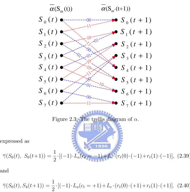
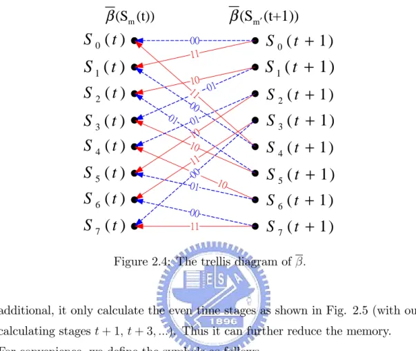
(21) Eq. (2.35) is obtained by removing the correction term and becomes max( ) maximum function. Replacing max ( ) by max( ) in (2.25), (2.26) and (2.27), we have the LLR with Max-Log-MAP. There is a small performance degradation by using LLR with MAX-Log-MAP instead of LLR with MAP. The degradation is more pronounced in low SNR region.. 2.3. Decoding Algorithm. 2.3.1. Radix-2 algorithm. In this section we use the trellis diagram to explain how ,. and. are calculated. in the radix-2 and the radix-4 algorithm. Fig. 2.3 and Fig. 2.4 show the trellis and. of. respectively, where the dotted lines and solid lines stand for ct = 0. and ct = 1. An example will help understand. Example 1: Calculation of. in radix-2 algorithm.. Referring to Fig 2.3 to obtained. (S0 (t + 1)), we know that there are two. paths connected to it. One path is S0 (t) ! S0 (t + 1) and the another path is. S1 (t) ! S0 (t + 1). Therefore (S0 (t); S0 (t + 1)) and (S1 (t); S0 (t + 1)) from. (2.33) can be expressed as (S0 (t); S0 (t+1)) =. 1 [( 1) La (ct = 2. 1)+Lc (rt (0) ( 1)+rt (1) ( 1)], (2.36). and (S1 (t); S0 (t+1)) =. 1 [(+1) La (ct = +1)+Lc (rt (0) (+1)+rt (1) (+1)]: (2.37) 2. Substituting (2.36) and (2.37) into (2.26) leads to (S0 (t + 1)) as follows (S0 (t + 1)) = max [ (S0 (t)) + (S0 (t); S0 (t + 1));. (S1 (t)) + (S1 (t); S0 (t + 1))]: (2.38). Example 2: Calculation of. in radix-2 algorithm.. Referring to Fig 2.4 to obtained (Sm (t), we know that there are two paths connected to it. One path is S0 (t + 1) ! S0 (t) and another path is S4 (t + 1) !. S0 (t). Therefore (S0 (t); S0 (t + 1)) and (S0 (t); S4 (t + 1)) from (2.33) can be 11.
(22) α (Sm′ (t+1)). α (Sm (t)). S 0 (t ). S1 (t ) S 2 (t ) S 3 (t ) S 4 (t ). S 0 ( t + 1). 00 11. 01. S 5 (t ) S 6 (t ). S 7 (t ). 10 11 01 00 01 10 10 11 00 10 01 00 11. S 1 ( t + 1) S 2 ( t + 1). S 3 ( t + 1) S 4 ( t + 1). S 5 ( t + 1) S 6 ( t + 1). S 7 ( t + 1). Figure 2.3: The trellis diagram of :. expressed as (S0 (t); S0 (t+1)) =. 1 [( 1) La (ct = 2. 1)+Lc (rt (0) ( 1)+rt (1) ( 1)], (2.39). and (S0 (t); S4 (t+1)) =. 1 [( 1) La (ct = +1)+Lc (rt (0) (+1)+rt (1) (+1)]: (2.40) 2. Substituting (2.39) and (2.40) into (2.27) leads to (S0 (t)) as follows (S0 (t)) = max [ (S0 (t+1))+ (S0 (t); S0 (t+1)); (S4 (t+1))+ (S0 (t); S4 (t+1))]: (2.41). 2.3.2. Radix-4 algorithm. In 2003, the radix-4 algorithm was proposed by M. Bickersta¤ [15] and has commonly used in hardware implementation, since the Radix-4 Log-MAP architecture doubling the throughput for a given clock rate over the radix-2 architecture. In 12.
(23) β (Sm′ (t+1)). β (Sm (t)). S 0 (t ). S 0 ( t + 1). 00 11. S1 (t ) S 2 (t ). 10 11 01 00 01 10 10 11 00 10 01. 01. S 3 (t ) S 4 (t ) S 5 (t ) S 6 (t ). S 1 ( t + 1). 00 11. S 7 (t ). S 2 ( t + 1). S 3 ( t + 1) S 4 ( t + 1). S 5 ( t + 1) S 6 ( t + 1) S 7 ( t + 1). Figure 2.4: The trellis diagram of :. additional, it only calculate the even time stages as shown in Fig. 2.5 (with out calculating stages t + 1; t + 3; :::). Thus it can further reduce the memory. For convenience, we de…ne the symbols as follows m t+k t+u+1 t+u (m; m). , (Sm (t + k)); , (Sm (t + u); Sm (t + u + 1));. and m t+k. , (Sm (t + k)):. Let us give an example to derive the recursive units Example 3: Calculating. 0 t+2. and. 0 t. and. for Radix-4 algorithm.. in Radix-4 algorithm.. 13.
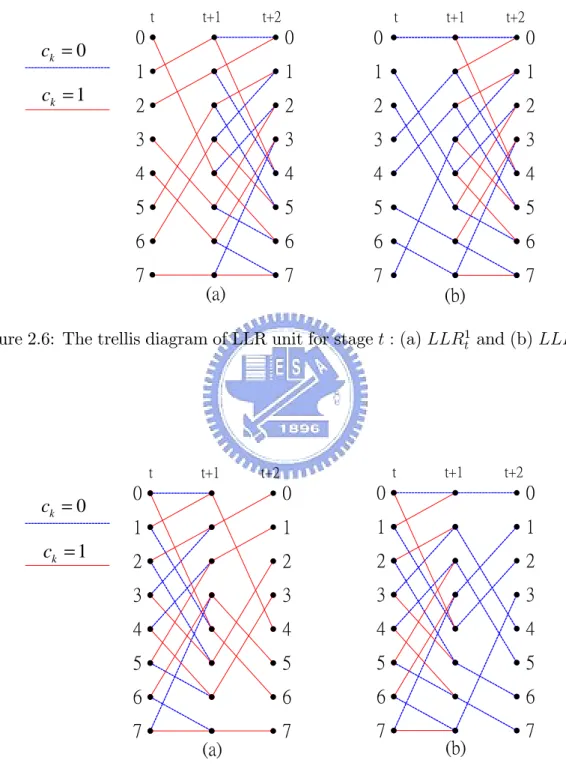
(24) 0 t+2. Referring to Fig. 2.5, 0 t+2. = max [. 0 t+1. t+2 t+1 (0; 0);. +. 0 t. and 1 t+1. are derived as follows t+2 t+1 (1; 0)]. +. = max fmax [. 0 t. +. t+1 t (0; 0);. 1 t. +. t+1 t (1; 0)]. +. t+2 t+1 (0; 0);. max [. 3 t. +. t+1 t (3; 1);. 2 t. +. t+1 t (2; 1)]. +. t+2 t+1 (1; 0)g. 0 t. = max fln[exp(. +. 3 t. ln[exp(. 0 t. = max fln[exp(. t+1 t (0; 0). t+1 t (1; 0)]. +. 2 t. + exp(. + exp(. t+2 t+1 (1; 0)). +. + ln[exp(. t+1 t (2; 1))]. +. t+2 t+1 (0; 0)). +. t+1 t (3; 1). +. 1 t. + exp(. t+1 t (3; 1)). +. +. 3 t. ln[exp(. t+1 t (0; 0)). 1 t. t+2 t+1 (1; 0))]g. + ln[exp( t+1 t (1; 0). +. 2 t. + exp(. t+2 t+1 (0; 0))],. t+1 t (2; 1). +. t+2 t+1 (0; 0))],. +. t+2 t+1 (1; 0))]g. +. = max fmax [. 0 t. +. t+1 t (0; 0). +. t+2 t+1 (0; 0);. 1 t. +. t+1 t (1; 0). +. t+2 t+1 (0; 0)];. max [. 3 t. +. t+1 t (3; 1). +. t+2 t+1 (1; 0);. 2 t. +. t+1 t (2; 1). +. t+2 t+1 (1; 0)]g;. (2.42) and 0 t. t+1 t (0; 4). = max [ = max f. +. 4 t+1 ;. t+1 t (0; 0). 0 t+1 ]. +. t+1 t (0; 4). + max [. t+2 t+1 (4; 2). +. 2 t+2 ;. t+2 t+1 (4; 6). +. 6 t+2 ];. t+1 t (0; 0). + max [. t+2 t+1 (0; 0). +. 0 t+2 ;. t+2 t+1 (0; 4). +. 4 t+2 ]g. = max fln[exp(. t+1 t (0; 4))]. + ln[exp(. t+2 t+1 (4; 2). +. 2 t+2 ). + exp(. t+2 t+1 (4; 6). +. 6 t+2 )],. ln[exp(. t+1 t (0; 0))]. + ln[exp(. t+2 t+1 (0; 0). +. 0 t+2 ). + exp(. t+2 t+1 (0; 4). +. 4 t+2 )]g. = max fln[exp( ln[exp( = max fmax [ max [. t+1 t (0; 4)). +. t+2 t+1 (4; 2). +. 2 t+2 )]. t+1 t (0; 0). +. t+2 t+1 (0; 0). +. 0 t+2 )]. t+1 t (0; 4)). +. t+2 t+1 (4; 2). +. 2 t+2 );. t+1 t (0; 0). +. t+2 t+1 (0; 0). +. 0 t+2 ;. t+1 t (0; 4)). + ln[exp(. + ln[exp(. t+1 t (0; 0). t+1 t (0; 4)) t+1 t (0; 0). +. +. +. +. t+2 t+1 (0; 4). t+2 t+1 (4; 6). t+2 t+1 (0; 4). t+2 t+1 (4; 6). +. +. +. 6 t+2 ];. 4 t+2 ]g:. (2.43). 2.3.3. Deriving LLR for Radix-4. Because we use radix-4 algorithm to decode two stages of soft information in one clock cycle, we need to use two LLR units. Let us derive LLR for stage t and stage t + 1. De…ne LLRtb as the LLR for ct = b, where b 2 (0; 1): For instance, 14. +. 6 t+2 )], 4 t+2 )].
(25) ct = 0 ct = 1. Stage t 0. Stage t+1. Stage t+2 0. Stage t 0. Stage t+2 0. 1. 1. 1. 1. 2. 2. 2. 2. 3. 3. 3. 3. 4. 4. 4. 4. 5. 5. 5. 5. 6. 6. 6. 6. 7. 7. 7. 7. Radix-2. Radix-4. Figure 2.5: The Radix-2 and Radix-4 trellis diagram.. 0 denotes the LLR for ct+1 = 0. LLRt1 denotes the LLR for ct = 1, and LLRt+1. Below, we derive the LLR for stage t. Referring to Fig. 2.6 and Fig. 2.7, we have LLRt1 = max( d. 0 t. +. t+1 t (0; 4). +. 4 t+1 ;. 1 t. +. t+1 t (1; 0). +. 0 t+1 ;. 2 t. +. t+1 t (2; 1). +. 1 t+1 ;. 3 t. +. t+1 t (3; 5). +. 5 t+1 ;. 4 t. +. t+1 t (4; 6). +. 6 t+1 ;. 5 t. +. t+1 t (5; 2). +. 2 t+1 ;. 6 t. +. t+1 t (6; 3). +. 3 t+1 ;. 7 t. +. t+1 t (7; 7). +. 7 t+1 );. 15. (2.44).
(26) Because in radix-4 algorithm we do not calculate 0. i. t+1 ,. we should replace. i t+1 ;. 7; by the trace-back values from stage t + 2 and rewrite (2.44) as follows. LLRt1 = max( d. 0 t. +. t+1 t (0; 4). + max (. t+2 t+1 (4; 2). +. 2 t+2 ;. t+2 t+1 (4; 6). +. 6 t+2 );. 1 t. +. t+1 t (1; 0). + max (. t+2 t+1 (0; 0). +. 0 t+2 ;. t+2 t+1 (0; 4). +. 4 t+2 );. 2 t. +. t+1 t (2; 1). + max (. t+2 t+1 (1; 0). +. 0 t+2 ;. t+2 t+1 (1; 4). +. 4 t+2 );. 3 t. +. t+1 t (3; 5). + max (. t+2 t+1 (5; 2). +. 2 t+2 ;. t+2 t+1 (5; 6). +. 6 t+2 );. 4 t. +. t+1 t (4; 6). + max (. t+2 t+1 (6; 3). +. 3 t+2 ;. t+2 t+1 (6; 7). +. 7 t+2 );. 5 t. +. t+1 t (5; 2). + max (. t+2 t+1 (2; 1). +. 1 t+2 ;. t+2 t+1 (2; 5). +. 5 t+2 );. 6 t. +. t+1 t (6; 3). + max (. t+2 t+1 (3; 1). +. 1 t+2 ;. t+2 t+1 (3; 5). +. 5 t+2 );. 7 t. +. t+1 t (7; 7). + max (. t+2 t+1 (7; 3). +. 3 t+2 ;. t+2 t+1 (7; 7). +. 7 t+2 )):. (2.45) Similarly LLRt1 and LLRt0 can be shown as follows LLRt0 = max( d. 0 t. +. t+1 t (0; 0). + max (. t+2 t+1 (0; 0). +. 0 t+2 ;. t+2 t+1 (0; 4). +. 4 t+2 );. 1 t. +. t+1 t (1; 4). + max (. t+2 t+1 (4; 2). +. 2 t+2 ;. t+2 t+1 (4; 6). +. 6 t+2 );. 2 t. +. t+1 t (2; 5). + max (. t+2 t+1 (5; 2). +. 2 t+2 ;. t+2 t+1 (5; 6). +. 6 t+2 );. 3 t. +. t+1 t (3; 1). + max (. t+2 t+1 (1; 0). +. 0 t+2 ;. t+2 t+1 (1; 4). +. 4 t+2 );. 4 t. +. t+1 t (4; 2). + max (. t+2 t+1 (2; 1). +. 1 t+2 ;. t+2 t+1 (2; 5). +. 5 t+2 );. 5 t. +. t+1 t (5; 6). + max (. t+2 t+1 (6; 3). +. 3 t+2 ;. t+2 t+1 (6; 7). +. 7 t+2 );. 6 t. +. t+1 t (6; 7). + max (. t+2 t+1 (7; 3). +. 3 t+2 ;. t+2 t+1 (7; 7). +. 7 t+2 );. 7 t. +. t+1 t (7; 3). + max (. t+2 t+1 (3; 1). +. 1 t+2 ;. t+2 t+1 (3; 5). +. 5 t+2 ):. (2.46) Finally, the LLR at stage t can be expressed as LLRt = LLRt1. LLRt0 :. (2.47). Similarly, the LLR at stage t + 1 can be expressed as 1 LLRt+1 = LLRt+1. 16. 0 LLRt+1 ;. (2.48).
(27) where 0 t. +. t+1 t (0; 0);. 1 t. +. t+1 t (1; 0)). +. t+2 t+1 (0; 4). +. 4 t+2 ;. max (. 2 t. +. t+1 t (2; 1);. 3 t. +. t+1 t (3; 1)). +. t+2 t+1 (1; 0). +. 0 t+2 ;. max (. 4 t. +. t+1 t (4; 2);. 5 t. +. t+1 t (5; 2)). +. t+2 t+1 (2; 1). +. 1 t+2 ;. max (. 6 t. +. t+1 t (6; 3);. 7 t. +. t+1 t (7; 3)). +. t+2 t+1 (3; 5). +. 5 t+2 ;. max (. 0 t. +. t+1 t (0; 4);. 1 t. +. t+1 t (1; 4)). +. t+2 t+1 (4; 6). +. 6 t+2 ;. max (. 2 t. +. t+1 t (2; 5);. 3 t. +. t+1 t (3; 5)). +. t+2 t+1 (5; 2). +. 2 t+2 ;. max (. 4 t. +. t+1 t (4; 6);. 5 t. +. t+1 t (5; 6)). +. t+2 t+1 (6; 3). +. 3 t+2 ;. max (. 6 t. +. t+1 t (6; 7);. 7 t. +. t+1 t (7; 7)). +. t+2 t+1 (7; 7). +. 7 t+2 );. 1 = max(max d ( LLRt+1. (2.49) and. 0 t. +. t+1 t (0; 0);. 1 t. +. t+1 t (1; 0)). +. t+2 t+1 (0; 0). +. 0 t+2 ;. max (. 2 t. +. t+1 t (2; 1);. 3 t. +. t+1 t (3; 1)). +. t+2 t+1 (1; 4). +. 4 t+2 ;. max (. 4 t. +. t+1 t (4; 2);. 5 t. +. t+1 t (5; 2)). +. t+2 t+1 (2; 5). +. 5 t+2 ;. max (. 6 t. +. t+1 t (6; 3);. 7 t. +. t+1 t (7; 3)). +. t+2 t+1 (3; 1). +. 1 t+2 ;. max (. 0 t. +. t+1 t (0; 4);. 1 t. +. t+1 t (1; 4)). +. t+2 t+1 (4; 2). +. 2 t+2 ;. max (. 2 t. +. t+1 t (2; 5);. 3 t. +. t+1 t (3; 5)). +. t+2 t+1 (5; 6). +. 6 t+2 ;. max (. 4 t. +. t+1 t (4; 6);. 5 t. +. t+1 t (5; 6)). +. t+2 t+1 (6; 7). +. 7 t+2 ;. max (. 6 t. +. t+1 t (6; 7);. 7 t. +. t+1 t (7; 7)). +. t+2 t+1 (7; 3). +. 3 t+2 ):. 0 LLRt+1 = max(max d (. (2.50). 2.4. Decoding Architecture. The decoder consists of two identical SISO decoders, interleavers and de-interleavers. The architecture is shown in Fig. 2.8. Applying (2.19) and (2.33), the SISO decoder can be derived as follows. 17.
(28) t. ck = 0. ck = 1. t+1. t+2. t. t+1. t+2. 0. 0. 0. 0. 1. 1. 1. 1. 2. 2. 2. 2. 3. 3. 3. 3. 4. 4. 4. 4. 5. 5. 5. 5. 6. 6. 6. 6. 7. 7. 7. (a). 7 (b). Figure 2.6: The trellis diagram of LLR unit for stage t : (a) LLRt1 and (b) LLRt0 :. t. ck = 0. ck = 1. t+1. t. t+2. t+1. t+2. 0. 0. 0. 0. 1. 1. 1. 1. 2. 2. 2. 2. 3. 3. 3. 3. 4. 4. 4. 4. 5. 5. 5. 5. 6. 6. 6. 6. 7. 7. 7. (a). (b). 7. 1 Figure 2.7: The trellis diagram of LLR unit for stage t + 1 : (a) LLRt+1 and (b) 0 LLRt+1 .. 18.
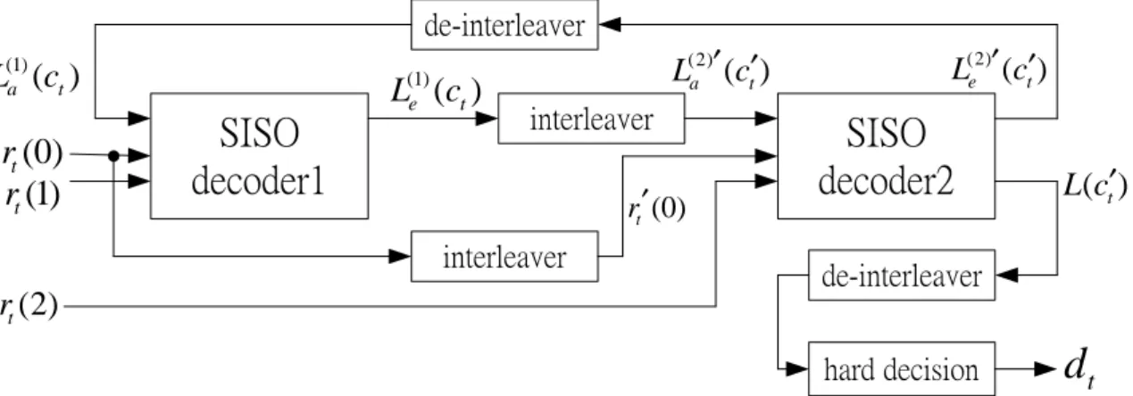
(29) de-interleaver (1) a. L (ct ). SISO decoder1. rt (0) rt (1). ′ ′ L(2) e (ct ). ′ ′ L(2) a (ct ). L(1) e (ct ). interleaver. SISO decoder2. rt′ (0). interleaver. L(ct′). de-interleaver. rt (2). dt. hard decision. Figure 2.8: An architecture of the turbo decoder.. P. L(ct ) = ln P. S(m;m)2c+1 t. S(m;m)2ct. P. = ln P. 1. e. (Sm (t))+ (Sm (t);Sm (t+1))+ (Sm (t+1). e. (Sm (t))+ (Sm (t);Sm (t+1))+ (Sm (t+1) 1. S(m;m)2c+1 t. S(m;m)2ct. e 2 [(+1) La (ct )+Lc rt (0) (1)] e 1. 1. e 2 [(. 1) La (ct )+Lc rt (0) ( 1)]. P. = La (ct ) + Lc rt (0) + ln P. S(m;m)2c+1 t. S(m;m)2ct. 1. e. (Sm (t))+ 12 (Sm (t))+ 12. e. (Sm (t))+ 21. e. (Sm (t))+ 12. = La (ct ) + Lc rt (0) + Le (ct ),. Pn. 1 i=1. Pn. 1 i=1. Pn. Lc rt (i)wt (i)+ (Sm (t+1). 1 i=1. Lc rt (i)wt (i)+ (Sm (t+1). Lc rt (i)wt (i)+ (Sm (t+1). Pn. 1 i=1. Lc rt (i)wt (i)+ (Sm (t+1). (2.51). where the Le (ct ) are called extrinsic information corresponding to ct : The Le (ct ) can be obtained from (2.51) as follows Le (ct ) = L(ct ). (2.52). [La (ct ) + Lc rt (0)]:. rt (0); rt (1) and rt (2) are the transmitter signals xt ; zt and z t after passing (1). AWGN channel respectively. Initially, we set the a priori information La (ct ) for (1). the …rst SISO decoder to zero. Then rt (0); rt (1), and La (ct ) are passed into the (1). …rst SISO decoder and obtain the extrinsic information Le (ct ) that can o¤er the (2). (1). next SISO decoder more accurate information for La (ct ). After Le (ct ) and r0 (t) (2). pass the interleaver, we obtain the signal La (ct ) and r0 (t) respectively. Similarly, (2). (2). the second SISO decoder can generate Le (ct ) and L(ct ) after the La (ct ), rt (0) 19.
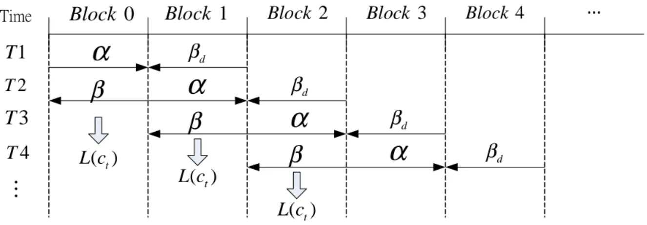
(30) Time. Block 0. Block 1. T1. α. βd. T2. β. α β. T3 T4. L(ct ). …. L(ct ). Block 2. Block 3. Block 4. .... βd. α. βd. α. β. βd. L(ct ) Figure 2.9: The sliding window diagram.. and rt (2) pass it. When the maximum allowable number of iterations is reached, dt can be obtained by de-interleavering L(ct ) and then take hard decision.. 2.4.1. Sliding Window. Theoretically, we need to calculate the LLR according to the whole received data in a block. However, when N is large, it is impractical to implement this ideal in a hardware since we need large memory and latency in this case. To reduce the memory and latency, a sliding window can be adopted [16]. In Fig. 2.9, the received data stream is divided into n blocks, the dummy backward recursion set initial value equal to value. d. is fed to. more accurate. log( N umber of1 the states ).. d. When a block is computed, the. for initial boundary value. The larger the block length is, the we will obtain. As soon as. d. is ready for a speci…ed received. data, we can obtain its corresponding L(ct ). At the same time, we can calculate for the next blocks. Repeat the same procedure, all of the data can be decoded.. 20.
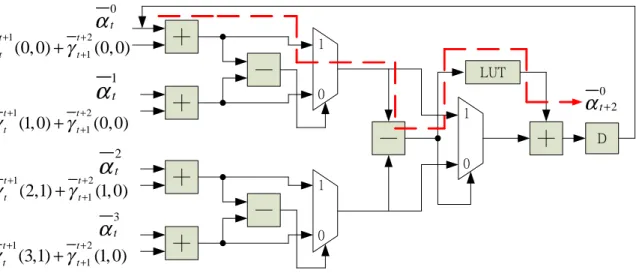
(31) Chapter 3 Radix-4 Recursive Architecture 3.1. Conventional Architecture. We derived. 0 t+2. in (2.42), however we must take recursive value of ( , ) approx-. imately (i.e. replace some max f g with maxf g) in hardware implementation. In [15], Lucent Bell Labs proposed the following approximation 0 t+2. 0 t. t max fmax[ max[. 3 t. +. +. t+1 t (0; 0) t+1 t (3; 1). +. +. t+2 t+1 (0; 0); t+2 t+1 (1; 0);. 1 t 2 t. +. +. t+1 t (1; 0) t+1 t (2; 1). +. +. t+2 t+1 (0; 0)]; t+2 t+1 (1; 0)]g:. (3.1) Fig. 3.1 is a radix-4 architecture for (3.1), the critical path (with dash line) consists of four multi-bit additions, one 2-to-1 MUX and one LUT, where the LUT is implemented using look-up table for correction term. In next section, we proposed an architecture for LUT which can reduce the critical path.. 3.2. Proposed Architecture. Because the hardware of the recursive unit in radix-4 is more complicated than that of radix-2, the critical path is too long so that it cannot achieve exactly twice of the throughput over radix-2. Thus our goal is to reach twice of the throughput while the area is as small as possible. From [20], Z. Wang proposed an architecture for high speed recursion and approximation for. 21. and. shown.
(32) 0. t +1. t +2. αt. γ t (0, 0) + γ t +1 (0, 0). α t +1. 1 LUT. 1 t. 0. 0. t +2. 1. γ t (1, 0) + γ t +1 (0,0) t +1. t +2. α. α t +2 D. 2 t. 0. γ t (2,1) + γ t +1 (1, 0). 1. 3. t +1. t +2. αt. 0. γ t (3,1) + γ t +1 (1, 0) Figure 3.1: Conventional Radix-4 Architecture.. as follows 0 t+2. t maxfmax [. 0 t. +. t+1 t (0; 0). +. t+2 t+1 (0; 0);. 1 t. +. t+1 t (1; 0). +. t+2 t+1 (0; 0)];. max [. 3 t. +. t+1 t (3; 1). +. t+2 t+1 (1; 0);. 2 t. +. t+1 t (2; 1). +. t+2 t+1 (1; 0)]g;. (3.2) and 0 t. = max fmax [ max [. t+1 t (0; 4)) t+1 t (0; 0). +. +. t+2 t+1 (4; 2) t+2 t+1 (0; 0). +. +. 2 t+2 ); 0 t+2 ;. t+1 t (0; 4)) t+1 t (0; 0). +. +. t+2 t+1 (4; 6). t+2 t+1 (0; 4). +. +. 6 t+2 ];. 4 t+2 ]g:. (3.3) Applying (3.2) to the hardware in Fig. 3.2. At the …rst stage we use carry save adder (CSA) to convert three additions to two additions. At last stage of Fig. 3.1 ,. 0 t+2. is divided into two parts as in Fig. 3.2. One is max( ). value and the other is the correction term that both are removed to the …rst stage adder, which is called O¤set-Add-Compare-Select (OACS) operation [19]. Conventionally, in LUT block we need to take a absolute value and then take table look-up. Therefore the computation time of the LUT is larger than the MUX marked with dash line. Hence the LUT dominates the critical path. In [20] a method was proposed to reduce computation time of the LUT. The computation 22.
(33) LUT. 0. αt A 0. t +1. 0. αt B. t +2. 1. γ t (0, 0) + γ t +1 (0, 0). t +1. t +2. α α. 1 tA 1 tB. α. 2 t A. 0. 0. LUT. 0. 1. 2. αt B. t +2. t +1. t +2. α t +2 A D. 1. γ t (2,1) + γ t +1 (1, 0) α α. α t +2 B D. γ t (1, 0) + γ t +1 (0, 0). t +1. 1. 0. 3 tA 3 tB. 0. γ t (3,1) + γ t +1 (1, 0). Figure 3.2: Radix-4 recursion architecture of [20]. time is reduced since it does not need to perform absolute operation. Let us explain as follows. In Fig. 3.3, assume the input of the LUT is a n-bits sign number, the g( ) function is used to detect the absolute vaue of the input which is less than 2:0, i.e. z = 1 of the input is less than 2:0. The ELUT block is a small LUT with 3-bits input and 2-bits output. It is used to simple the logic design. Table 3.1 shows the LUT approximation where x and g(x) are the quantized input and output of ELUT. The …nal output of the LUT is d1 and d0 : The general form of z can be derived as follows: z = bn. 1. bn. 2. + bn 3 ; :::; +b3 + f (bn. 1. = 1; bn. 2; :::; b1 ; b0 ),. d1 = z c1 and d0 = z c0 , where f ( ) is a combination circuit that consists of bn. 2; :::; b1 ; b0. when bn. 1. = 1:. The proposed structure of LUT is in Fig. 3.4. The inputs of the LUT are quantized to integer number and then use simple logic design to obtain the output. 23.
(34) jxj g(x). 0.0 0.5 1.0 1.5 > 2 0.75 0.5 0.25 0.25 0. Table 3.1: Approximation of [20].. bn −1 bn −2. bn −3. • •. •. • •. •. b3. b2. g (⋅). b1. b0. ELUT. c1. c0. z. d1. d0. Figure 3.3: Architecture of the proposed LUT used in [20].. In Table 3.2, we observe the dynamic range of the input can be divided as [-1 -0.25], [-2 -1.25], [0 0.75] and [1 1.75] and use combination logic to obtain the output p1 and p0 , which is independent of b1 and b0 . Therefore we do not need to take care of part of the input signal, and the logic gate can somewhat be. The performance comparison for various algorithm is as shown in Fig. 3.5, we see the proposed method and Arch-Z achieve nearly the same performance. The approximated values of the proposed method are given by 8 1 v<1 < 0:5, 0:25, 2 v < 1 or 1 v < 2 u(v) = : 0, otherwise. ;. (3.4). where v and u(v) are the input and output of the proposed LUT. In (3.4), we eliminate that u(v) equal to 0.75 (compared to Table 3.1), if we consider the case that u(v) equal to 0.75, we …nd the output p0 is dependent of b1 and b0 . Thus we ignore the value 0.75 of u(v). In section 3.3, the comparison of the proposed LUT and the LUT is shown in Table 3.1. The BER performance with the two 24.
(35) bn −1 bn −2. bn −3. • •. •. • •. •. b3. b2. b1. b0. combinational logic. p1. p0. Figure 3.4: Architecture of the proposed LUT.. LUT are nearly same. In Fig. 3.4, p1 and p0 are used to simplify the combination logic shown as follows p 1 = bn. 1. ::: b3 b2 + bn. 1. ::: b3 b2. p 0 = bn. 1. ::: b3 b2 + bn. 1. ::: b3 b2 :. and. We give an example to compare the two LUTs as follows Example 4: Refer to Table. 3.2, Fig. 3.3 and Fig. 3.4, assume the input bitlength of the LUT is 13, and that of the output is 2 . We de…ne the notations as follows b[12 : 0] : input of the LUT which is 13-bit with the 2 LSBs be the fractional bits. [c1 c0 ] : output of the ELUT consisting of simple combination. [d1 d0 ] : output of the LUT in [20]. [p1 p0 ] : output of the LUT in the proposed method. (1). The method in [20]: z is given by z = b12 b11 ::: b4 b3 + b12 b11 ::: b4 b3 (b2 + b1 + b0 ), c1 = b12 + b2 + b13 b2 (b1 + b0 ); and c0 = (b12 + b2 ) b12 b2 (b1 25. b0 ):.
(36) The out results of the LUT is d1 = z c1 ; and d0 = z c0 : (2). The proposed method: the output [p1 p0 ] of the LUT is as follows p1 = b12 b11 ::: b3 b2 + b12 b11 ::: b3 b2 ,. (3.5). p0 = b12 b11 ::: b3 b2 + b12 b11 ::: b3 b2 :. (3.6). and. From (3.5) and (3.6), we …nd that p1 and p0 have common terms and the logic can share the common terms to reduce complexity. De…ne the following two terms: COM B1 = b12 b11 ::: b3 and COM B2 = b12 b11 ::: b3 = b12 + b11 + ::: + b3 : Rearrange (3.5) and (3.6), we have p1 = COM B1 b2 + COM B2 b2 ; and p0 = COM B1 b2 + COM B2 b2 :. 3.2.1. Performance Comparison. We compare …ve recursive architectures (including the proposed one) in terms of their critical path, area and throughput as shown in Table. 3.3. The architectures used for comparison are explained as follows:. 26.
(37) Binary of input b[12 : 0] .. . 1111111110111 1111111111000 1111111111001 1111111111010 1111111111011 1111111111100 1111111111101 1111111111110 1111111111111 0000000000000 0000000000001 0000000000010 0000000000011 0000000000100 0000000000101 0000000000110 0000000000111 0000000001000 0000000001001 .. .. Decimal q(x) .. 0 . -2.25 0 -2 0 -1.75 0.25 -1.5 0.25 -1.25 0.25 -1 0.25 -0.75 0.5 -0.5 0.5 -0.25 0.75 0 0.75 0.25 0.75 0.5 0.5 0.75 0.5 1 0.25 1.25 0.25 1.5 0.25 1.75 0.25 2 0 2.25 0 .. . 0. d1. d0. u(v) p1. p0. 0 0 0 0 0 0 0 1 1 1 1 1 1 0 0 0 0 0 0 0. 0 0 0 1 1 1 1 0 0 1 1 1 0 0 1 1 1 1 0 0. 0 0 0.25 0.25 0.25 0.25 0.5 0.5 0.5 0.5 0.5 0.5 0.5 0.5 0.25 0.25 0.25 0.25 0 0. 0 0 0 0 0 0 1 1 1 1 1 1 1 1 0 0 0 0 0 0. 0 0 1 1 1 1 0 0 0 0 0 0 0 0 1 1 1 1 0 0. 0. 0. 0. 0. 0. Table 3.2: The values of g(x); u(v); d1 ; d0 and p1 ; p0 . (1). Arch-O: traditional radix-2 architecture. (2). Arch-L: the radix-4 architecture proposed by Lucent [15]. (3). Arch-Y: the radix-4 architecture proposed by [21]. (4). Arch-Z: the radix-4 architecture proposed by [20]. We …nd that Arch-Y has the largest area and the fastest throughput rate, its approximation is the same as in (3.1). Thus the performance degradation is large. In Example 4, we compared Arch-Z and the proposed scheme, Assume that AND, OR ,XOR and NOT gates have the same delay time (one unit time), the delay time in Arch-Z is about f ive unit times and that of the proposed scheme 27.
(38) Architecture Arch-O Arch-L [15] Arch-Y [21] Arch-Z [20] Proposed. Maximum Clock Freq. 286 217 240 231 232. Relative Area 1 1.53 3.08 1.83 1.80. Relative Throughput 1 1.52 1.68 1.62 1.62. Power Consumption 3.5478 mW 4.4691 mW 8.5570 mW 5.2784 mW 5.2839 mW. Table 3.3: Comparison of various recursive architectures. is about f our unit times. Therefore our propose method can somewhat reduce the critical path. As a result the clock rate can be somewhat increased, and the power consumption and BER performance (see Fig. 3.5) are nearly the same.. 3.3. Fixed point Analysis. Table 3.4 shows the quantization format of the Proposed scheme. Fig. 3.5 also shows the …xed-point performance of the proposed scheme. We see that the MaxLog-MAP degrade the performance about 0.4dB of Log-MAP. In Arch-L, because his method only use an LUT, which leads to less accuracy, its performance is worst than Arch-Z and the proposed one. In addition, the proposed scheme has worse performance than the Log-MAP by only 0.025dB. The …x-point simulation, we …nd the performance is smaller than 0.1dB compared with log-MAP. Functions n Word Length Received Bits Channel Reliable (Lc ) State Metrics ( , ) Branch Metrics ( ) Extrinsic (Lex ) LLR. Integer Parts (include sign bit) Fraction Parts 2 2 2 2 8 2 8 2 6 2 10 2. Table 3.4: Quantization format for the proposed Turbo Decoder.. 28.
(39) Figure 3.5: Performance comparison among the Log-MAP and four approximated algorithms.. 29.
(40) Chapter 4 VLSI Implementation. In this chapter, we describe the decoding ‡ow with hardware architecture and show the chip layout as well as the corresponding chip performance comparison.. 4.1. Hardware Design for 3GPP. Fig. 4.1 is the overall turbo decoder architecture. Because we use radix-4 algorithm to decode data, we can deal with two stages of data per clock cycle. In order to achieve this goal, we can use Dual-RAM which can either read or write two samples of data per clock cycle. However using Dual-RAM doubles the memory area as well. In the proposed VLSI scheme, we will use one Single-RAM which can either read or write one sample of data per clock cycle, we divide this Single-RAM into two smaller RAMs to save even indexed data and odd indexed data. Below, we describe the subblock of decoder operation.. 4.1.1. Input Bu¤er. In Fig. 4.2, there are two paths, path 1 is for SISO Decoder 1 and path 2 is for SISO Decoder 2. In the beginning, the input data (rt (0); rt (1) and rt (2)) are saved in RAM1, RAM3 and RAM4, and rt (0) is fed to Interleaver and then the output of the interleaver are saved in RAM2. We proposed a solution to save memory. In the proposed scheme, we divide one Single-RAM into two smaller RAMs to save even indexed data and odd indexed data. Also, the ROM in interleaver is divided. 30.
(41) SISO Decoder. Input Buffer. BMU. A Prior Information. OACS. Hard decision. LLR. Extric Information. Deinterleaver. Interleaver/Deinterleaver. Figure 4.1: The turbo decoder architecture with a single SISO decoder.. into smaller ROMs to save even indexed address and odd indexed address. We take two address (Address 1 and Address 2) from two smaller ROMs (Sub-ROM (E) and Sub-ROM (O), where E for even and O for odd) as shown in Fig. 4.3. 1 2 Refering to Fig. 4.4, the data corresponding to b Address c and b Address c is saved 2 2. in Sub-RAM2 (E) and Sub-RAM2 (O), and according to Address 1 and Address 2 within two clock cycles, we have the following four cases 1. Case 1: Address 1 is even number and Address 2 is odd number. Address 1 is equal to 500 at T0 and it corresponds to the address 250 (b 500 c) 2. in Sub-RAM2 (E). Thus it enables sub-RAM2 (E) and disables sub-RAM2 (O). Then d0 is saved to sub-RAM2 (E) at address 250. Address 2 is equal to 201 at T1 and it corresponds to the address 100 (b 201 c) in Sub-RAM2 2 (O). Thus it disables sub-RAM2 (E) and enables sub-RAM2 (O). Then d1 is saved to sub-RAM2 (O) at address 100. 2. Case 2: Address 1 is odd number and Address 2 is even number. Address 1 is equal to 211 at T2 and it corresponds to the address 105 in Sub-RAM2 (O). Thus it enables sub-RAM2 (O) and disables sub-RAM2 (E). Then d2 is saved to sub-RAM2 (O) at address 105. Address 2 is equal 31.
(42) Number of Address1 even odd even odd even odd even odd. T(0; 2; :::) Number of Input of Sub-RAM2(E) Input of Sub-RAM2(O) Address2 1 odd b Address c 2 1 even b Address c 2 1 c even b Address 2 1 c odd b Address 2 T(1; 3; :::) 2 even b Address c 2 Address 2 odd b c 2 Address 2 even b c 2 2 odd b Address c 2. Table 4.1: Summary of interleaver process with four case. to 510 at T3 and it corresponds to the address 255 in Sub-RAM2 (E). Thus it disables sub-RAM2 (O) and enables sub-RAM2 (E). Then d3 is saved to sub-RAM2 (E) at address 255. 3. Case 3: both of Address 1 and Address 2 are even number. At T4 and T5 , Address 1 is 520 and Address 2 is 530. Therefore d4 and d5 will be saved to sub-RAM2 (E). Thus we enable sub-RAM2 (E) and disable sub-RAM2 (O). Then, d4 and d5 are saved in sub-RAM2 (E) at address 260 and 265. 4. Case 4: both of Address 1 and Address 2 are odd number. At T6 and T7 , Address 1 is 221 and Address 2 is 301. Therefore d6 and d7 will be saved to sub-RAM2 (O). Thus we enable sub-RAM2 (O) and disable sub-RAM2 (E). Then, d6 and d7 are saved in sub-RAM2 (O) at address 110 and 150. We summary the interleaver process with four cases as in Table 4.1, where the notation. denotes don’t care.. Table 4.2, is a comparision of input bu¤er implemented by Single-RAM and Dual-RAM. From the table, if we use the Dual-RAM the area is larger than the 32.
(43) BMU ( β d ). Path 1. rt (0) RAM1. rt (0) Interleaver ROM. rt′ (0). RAM2. LIFO (A). Path 2 Path 1. LIFO (B). rt (1). rt (1). RAM3. rt (2). RAM4. rt (2) Path 2 Path 1. SISO Decoder 1. Path 2. SISO Decoder 2. Figure 4.2: The input data ‡ow. Relative area Relative power Single-RAM (proposed) 1 1 Dual-RAM 2.37 3.55. Table 4.2: Comparision of area and power for implementing the input bu¤er by dual-RAM and singl-RAM. Single-RAM by 2.37 times, and the power is larger than the Single-RAM by 3.55 times. Thus our proposed method reduced the area and power signi…cant.. 33.
(44) Interleaver ROM. SubROM(E). SubROM(O). Address1. RAM2. Address2 MUXA. MUXB. SubRAM2(E). SubRAM2(O). Figure 4.3: The proposed ROM and RAM scheme to achieve two-read and twowrite in one clock cycle.. 4.1.2. BMU(branch metric unit ). The BMU is used to computate the branch metrics : The BMU correspond to equation is (2.33). In 3GPP std.,. can as shows as follows. 1 = [La (ct )) (rt (0) + rt (1))]; 2 1 t+1 t+1 t+1 t+1 rt (1))]; t (2; 1) = t (3; 5) = t (6; 4) = t (5; 2) = [La (ct )) + (rt (0) 2 (4.1) t+1 t (0; 4). =. t+1 t (1; 0). =. t+1 t (6; 3). =. t+1 t (7; 7). and t+1 t (0; 0). =. t+1 t (1; 4). =. t+1 t (6; 7). =. t+1 t (7; 3). =. t+1 t (0; 4);. t+1 t (2; 5). =. t+1 t (3; 1). =. t+1 t (4; 2). =. t+1 t (5; 6). =. t+1 t (2; 1):. t+1 t (0; 4),. t+1 t (2; 1),. In (4.1) and (4.2), we only calculate and the other. t+1 t (0; 0). and. (4.2) t+1 t (2; 5). can obtained.from these four values. Fig. 4.5 shows a hardware. architecture for . Here we ignore divide-by-2, because in VLSI implementation divide-by-2 operation is just a shift operation. 34.
(45) CASE 1. CASE 2. CASE 3. CASE 4. T0. T1. T2. T3. T4. T5. T6. T7. d0. d1. d2. d3. d4. d5. d6. d7. Address1. 500. 500. 211. 211. 520. 520. 221. 221. Address2. 201. 201. 510. 510. 530. 530. 301. 301. Address of Sub-RAM2(E). 250. x. x. 105. 260. 265. x. x. 255. x. x. 110. 150. rt (0). Address of Sub-RAM2(O). x. 100. x. d5. d5. d5. d4. d4. d4. d4. d3. d3. d3. d3. d3. d0. d0. d0. d0. d0. 265 260. Sub-RAM2(E). 255 250. d0. d0. d0. 150 110. Sub-RAM2(O). 105 100. d1. d7. d6. d6. d2. d2. d2. d2. d2. d2. d1. d1. d1. d1. d1. d1. Figure 4.4: Timing diagram for the proposed RAM and ROM schemes.. 35.
(46) 0. rt (1). t +1. rt (0). γ t (0, 0). La (ct ). γ t (0, 4). t +1. 0. rt (1). t +1. rt (0). γ t (2,5). La (ct ). γ t (2,1). t +1. Figure 4.5: The architecture of :. 4.1.3. OACS(O¤set-Add-Compare-Select). The OACS is used to calculate. d;. and . The architecture is shown in Fig.. 3.2. Since the OACS is a recursive unit, its computation result will increase after each iteration. Hence the …nal result may saturate. In order to overcome this situation, we adopt the normalization scheme proposed in [21]. Fig. 4.6 shows an example for. 0 t+2. with normalization. When one of the values,. 0 t+2, A. s. 7 t+2, A ;. are large than or equal to 2L 2 , where L is the word length of the state metrics (. (0s7) t+2, A. and. (0s7) t+2, A )),. we subtract 2L. 2. from all of the state metrics to avoid. saturation.. 4.1.4. LLR (Log-Likelihood Ratio ). The LLR output for the radix-4 turbo decoder can be calculated according to (2.48)-(2.50) and the corresponding hardware is shown in Fig. 4.7, where max (see (2.23)) can be express as hardware shown in Fig. 4.8, and the LUT is the proposed structure in section 3.2. In LLR unit, we used pipeline skill to reduce the critical path with the penalty of increasing 28 registers. The processing time for each SISO decoding is three clock cycles.. 36.
(47) LUT. 0. αt A. t +1. t +2. α. 0 tB. γ t (0,0) + γ t +1 (0, 0). 0. 1. 1. 0. 0. α t +2 B D. 1. t +1. t +2. αtA 1 αtB. γ t (1, 0) + γ t +1 (0,0) α t +1. t +2. α. LUT. 1. 2 tA. 2 tB. 1. γ t (2,1) + γ t +1 (1,0) 3. αt A 3 α tB t +1 t +2 γ t (3,1) + γ t +1 (1, 0). 1. 0 0. 0. α t +2 A α t +2 A 2. α t +2 A 3. α t +2 A 4. Normali-. α t + 2 A zation 5 α t +2 A. D. 6. α t +2 A 7. α t+2 A. Figure 4.6: The normalization of OACS.. 4.1.5. Extrinsic Information and a Priori Information. When the computation of LLR is completed, we calculate Le (ct ) refer to (2.52). Le (ct ) is to be sent to interleaver/de-interleaver and then saved as the a Priori information. The a Priori information is saved in two RAMs, where we use two Dual-RAMs to achieve this, because adopting one Dual-RAM will lead to data hazard. Fig. 4.9 is the timing diagram for read/write situation in Dual-RAM 1 and Dual-RAM 2. Assume the data block length is ND and the window legnth is NL , operating at SISO decoder 1. At SISO decoder 1 period, the Dual-RAM 1 is in write-mode and the Dual-RAM 2 is in read-mode. At T0 , a priori information is read from Dual-RAM 2 to calculate the extric information and then obtain extric information e4 and e5. The e4 and e5 are passed into interleaver and then are saved to dual-RAM 1 at Address 1 and Address 0. Here if we adopt one Dual-RAM at T2 , we will extract a priori information at Address 0 and Address 1, however this a priori information has been updated at T0 . Therefore we need to. 37.
(48) max *. max *. max *. max *. max *. max *. max *. max * Pipeline Stage1. max *. max *. max *. max *. max *. Pipeline Stage2. max * Pipeline Stage3. max * LLR. max * Pipeline Stage3. max * max *. max * max *. max *. max *. Pipeline Stage2 Pipeline Stage1. max *. max *. max *. max *. max *. max *. max *. Figure 4.7: The Architecture of LLR.. LUT. 1. 0. Figure 4.8: The hardware architecture of max ( ):. 38. max *.
(49) SISO decoder 1 period. Window Block Time Extric Information Address Dual-RAM 1 (write) Dual-RAM 2 (read). W0 T2. e0. WNL-1. T1. e1. e2. T0. e3. e4. T(NL-1)*3+2. T(NL-1)*3+1. T(NL-1)*3. e5. eND-6. eND-5 eND-4. eND-3. eND-2. eND-1. ND-6. ND-5. ND-3. ND-2. ND-1. 0. 1. 2. 3. 4. 5. e5. e4. e3. e2. e1. e0. eN -1 eN -2 eN -3 eN -4 eN -5 eN -6. a0. a1. a2. a3. a4. a5. aN -6 aN -5 aN -4 aN -3 aN -2 aN -1. D. D. D. D. ND-4 D. D. D. D. D. D. D. D. Figure 4.9: Timing diagram of a priori information for two Dual-RAMs.. save extric information e4 and e5 to Dual-RAM 2 to avoid data hazard. Operating at SISO decoder 2 period, the Dual-RAM 1 is in read-mode and the Dual-RAM 2 is in write-mode, its operation is similar with that in SISO decode 1 period.. 4.1.6. Interleaver and De-interleaver. The Interleaver has two purposes. One is to interleave rt (0) mentioned in Input Bu¤er. The other is to interleave Le (ct ) mentioned in Extrinsic Information and a Priori information. De-interleaver is used to de-interleave Le (ct ). In Input Bu¤er, we only use interleaver once. Then the interleaver is used to interleave Le (ct ) in iteration procedure. Hence we only need one interleaver. Since we need to use it several times in iteration process and only once to de-interleaver the output the LLR. Also, we only need one de-interleaver.. 4.1.7. Hard Decision. The number of iteration is in general limited, when the number of limitation iteration is reached, the output of the LLR will take hard decision (refer to (2.34) ) to decode two information bits. Fig. 4.10 is an architecture for the hard decision, assuming the LLR has n bits. We only consider the sign bit of the LLR. If the. 39.
(50) bn−1 bn− 2 bn −3. 0. • •. •. b0. 1 dt. 1. 0. Figure 4.10: The architecture of hard decision.. sign bit is 1, the output is 0; otherwise the output is 1.. 4.1.8. Sliding Window. Here we describe the sliding window approach. Referring to Fig. 4.11 and Fig 4.12, after all of the data are saved to RAM in Input Bu¤er. Then the data are taken from RAM1 and RAM3 /RAM2 and RAM4 and saved in LIFO (A) for SISO Decoder 1/SISO Decoder 2. The data LIFO (A) are then shift to LIFO (B). At the begining, we delay k=2 (k is window length) clock cycles to take data from RAM with data address from k=2. 1 to 0 and save them in LIFO(A). In second. k=2 clock cycles, we take data from RAM with data address from k. 1 to k=2,. and save them in LIFO(A). At this duration, take data from the input bu¤er and LIFO(A) and then fed to BMU ( d ) and BMU ( ) to calculate branch metrics. d. and . In the third k=2 clock cycles, the data in LIFO (B) is fed to BMU ( ) to calculate branch metric . The OACS ( d ) and OACS ( ) is calculated at second the k=2 clock cycles, and the calculated end of the second k=2 clock cycles,. d. d. and. is saved in bu¤er ( ). At the. is ready to calculate. the third k=2 clock cycles, we obtain a boundary value. d. by OACS ( ). In. to begin to calculate ,. and output . At the third k=2 clock cycles, all of the data (i.e.. ,. and ) are. fed to LLR to decide the soft information. If the number of iteration limitation is reached, we stop the process and fed the output of the LLR to hard decision and then perform De-interleaving for the decoded information bits.. 40.
(51) rt (0) / rt′ (0). BMU ( β d ). OACS ( β d ). LIFO (A). BMU (α ). OACS (α ). buffer (α ). LIFO (B). BMU ( β ). OACS ( β ). LLR. rt (1) / rt (2). Figure 4.11: Calculating BMU, OACS and LLR.. 4.2. Design ‡ow. In the section, we will introduce the design ‡ow for the proposed turbo decoder. The cell-based design ‡ow is as shown in Fig. 4.13.. 4.2.1. System model. First the encoder is created according to the 3GPP standard, and we use the proposed architecture to decoder. The simulation platform was built on Matlab. In VLSI impelmentation, we quantize the ‡oating-point to …xed-point and adjust the bit length so that the BER performance is close to ‡oating-point simulation result. When the bit length is decided, we can generate input and output test patterns for RTL. Using tool: Matlab.. 41.
(52) Time. k/2. k/2. k/2. k/2. Input data. Block 1 Block 2 Block 3 Block 4. LIFO (A). Block 1 Block 2 Block 3. LIFO (B). Block 1 Block 2 βd (Block 2). βd (Block 3). βd (Block 4). α (Block 1). α (Block 2). α (Block 3). β (Block 1). β (Block 2). α (Block 1). α (Block 2). LLR. LLR. buffer (α ). (Block 1) (Block 2). Figure 4.12: Timing diagram of Sliding Window.. 42.
(53) Specification development System model. System model (Matlab). RTL verification. RTL code (Verilog). Bit ture simulation NC-verilog and modelsim. Logic systhesis (Design complier). Gate level netlist. Gate Level pre-layout verification. Scan chain with netlist (DFT complier) Fault coverage analyze (TetraMax) Gate level simulation (NC-verilog). Place & Route (SOC Encounter). Gate Level post-layout verification Gate level STA. Layout Merging (Calibre). Layout verification (DRC/LVS). Layout verification (DRC/LVS). Circuit Extraction. Circuit -level simulation. Power analyze. Circuit Level verification Circuit -level STA. Tapeout. Figure 4.13: IC design ‡ow.. 43. RC Extraction Delay Calculation.
(54) 4.2.2. RTL code. We use Verilog-HDL to describe the hardware architecture. The general design method is hierarchically method. Hence we need to divide the overall design into serval basic modules …rst. Then, connecting among the basic modules to complete the rough structure. Finally we need to perform bit true in order to make sure the output signals of RTL code and Matlab are same with same input signals. In addition, we have using memory in our architecture, so we use the memory compiler to generate. Using tools: memory compiler, NC-verilog, modelsim, and Debussy nWave.. 4.2.3. BIST. Because there are memory in our architecture, we need to add BIST circuit on memory control for the testability of IC. After adding BIST circuit, there are two mode in circuit, i.e. function mode and test mode. Function mode means that normal Turbo decoding can be performed, and test mode can be used test that there are have any error in memory. Using tool: TurboBIST.. 4.2.4. Synthesis. In this step, we start to synthesize our circuit. Before this step, our program is just hardware language, is not real gate. By using Synopsys Design Compiler to do the synthesis, our program can be translate as real gate. And we can get the rough area and some timing information of the gate. In our decoder design, all modules except the one port and two port register …les are synthesized with TSMC 0:18 m CMOS process technology. Using tool: Design Compiler.. 4.2.5. Gate-level simulation. After synthesis, we can get timing information of gate. So we can perform our circuit to check have any error with real time. We use NC-Verilog to do the 44.
(55) gate-level simulation and use Debussy nWave to check waveform. By checking waveform, we can observe function exactitude with our predetermined clock period. Using tools: NC-Verilog, and Debussy nWave.. 4.2.6. DFT. For IC testing, we need to add mux in front of Flip-Flop and scan chains for the testability of IC. After adding mux, we can get there is any error between Flip-Flop and Flip-Flop by passing mux input signal. We use to Synopsys DFT Compiler to do scan chain insertion. Using tool: DFT compiler.. 4.2.7. ATPG. In the step, we use ATPG (automatic test pattern generator) of Synopsys TetraMax to generate test patterns for chip measurement. Using tool: Synopsys TetraMax.. 4.2.8. APR. We use SOC encounter to do automatical placement and routing (APR). Before placing and routing, we need to add power I/O and core I/O on Gate-level netlist and arrange location of input, output, I/O power, and core power on pad CIC supported. We need to consider core utilization, location of one port and two port register …les, number of power ring, location and number of stripe to meet timing constraints from SDC …le. Using tool: SOC encounter.. 4.2.9. DRC and LVS. In general, we usually have consider DRC (design rule checking) and LVS (layout V.S. schematic) in APR. But there is just rough check result in SOC encounter. So we need to do detail veri…cation. We use the Calibre DRC to check whether. 45.
(56) there is any error with design rule and use the Calibre LVS to make sure that whether the layout and the schematic are identical or not. Using tool: Calibre.. 4.2.10. Post-layout level. In order to check function, we take the netlist and …le of timing information generated by SOC encounter to run NC-Verilog. We can observe wave to …nd whether is any error by Debussy nWave. This is the last step to check function on myself work. Using tools: NC-Verilog, and Debussy nWave.. 46.
(57) BMU. Input Buffer. α. Dual-RAM ( Lex). Dual-RAM ( Lex). LLR. OACS. Buffer. Figure 4.14: Chip layout of the proposed Radix-4 Turbo Decoder for 3GPP.. 4.3. Chip Layout and Comparison. The turbo decoder is implemented by using the TSMC 0:18 m 1P6M CMOS process. It achieves the maximum clock rate of 167MHz. The chip layout is shown in Fig. 4.14 and the chip summary is also listed in Table 4.3. Comparing to [15], [23] and [24] as shown in Table 4.4, the core size and area of the proposed scheme is relative high. However the proposed scheme can achieve higher clock rate. In our proposed, the throughput is worst than the [15], but faster than the [23] and [24].. 47.
(58) Technology Chip size Core size Gate count Embedded SRAM Embedded ROM Clock rate Power consumption. TSMC 0.18 m 1P6M CMOS 7.28 mm2 2.65 mm2 200K 28K bits 9K bits 167 MHz 135mW. Table 4.3: The expected turbo decoder chip summary.. Technology Block Length Core Size (mm2 ) Clock Rate (MHz) Throughput (Mb/s) Number of iteration Energy e¢ ciency (nJ/b/iter.). [15] 0.18 m 5114 14.5 145 24 6 10. [23] 0.25 m 5114 9 135 5.48 6 6.98. Table 4.4: Chip comparison.. 48. [24] 0.18 m 5114 9 88 2 10 14.60. Proposed design 0.18 m 512 2.65 167 22 6 1.02.
(59) Chapter 5 Conclusion In this thesis, we proposed a LUT architecture, so the speed of MUX and LUT are nearly the same. As a result, the critical path is reduced. Because the decoder uses the Radix-4 algorithm, which deals with 2 stages of data in one clock cycle, we proposed a ROM and RAM read/write scheme to avoid the use of Dual-RAM. In chip implementation, the chip is fabricated in TSMC 0.18 m CMOS process, operating at 167MHz clock rate with voltage supply 1.62V. The power consumption is 135mW at decoding rate 22Mb/s with code rate 1/3 for 3GPP standard. The core area is 2.65 mm2 , contains 200K gate counts.. 49.
(60) Reference [1] C. Berrou, A. Glavieux, P. Thitimajshima, “Near Shannon limit errorcorrecting coding and decoding:Turbo-Codes,” Proc. of IEEE ICC’93, Geneva, pp. 1064-1070, Volume 2, May 1993. [2] TIA/EIA/CDMA2000, “Physical layer standard for CDMA-2000 standards for spread spectrum systems,”June, 2000. [3] “Technical Speci…cation Group Radio Access Network, Multiplexing and channel coding (FDD) (TS 25.212 V8.2.0)” 3rd Generation Partnership Project (3GPP). [4] J. Hagenauer and P. Hoeher, “A Viterbi algorithm with soft-decision outputs and its applications,”in Proc. IEEE GLOBECOM, Dallas, TX, pp. 47.1.1– 47.1.7, Nov. 1989. [5] J. Hagenauer et al., “Decoding turbo codes with the soft-output Viterbi algorithm (SOVA),”in Proc. IEEE Int. Symp. Information Theory, Trondheim, Norway, pp. 164, 1994. [6] L. Papke and P. Robertson, “Improved decoding with the SOVA in a parallel concatenated (turbo-code) scheme,”in Proc. IEEE Int. Conf. Communications, pp. 102–106, 1996. [7] P. Robertson, E. Villebrun, and P. Hoeher, “A comparison of optimal and suboptimal MAP decoding algorithms operating in the log domain,”in Proc. IEEE Int. Conf. Communications, pp. 1009–1013, 1995.. 50.
(61) [8] J. Vogt and A. Finger, “Improving the MAX-LOG-MAP turbo decoder,” Electron. Lett., vol. 36, pp. 1937–1939, Nov. 2000. [9] J. Hagenauer et al., “Iterative (turbo) decoding of systematic convolutional codes with the MAP and SOVA algorithms,” in Proc. ITG, Munich, Germany, pp. 21–29, Oct. 1994. [10] M. Shin and I.-C. Park, “Processor-based turbo interleaver for multiple thridgeneration wireless standards,”IEEE Commun. Lett., vol. 7, no. 5, pp. 210– 12, May 2003. [11] P. Ampadu and K. Kornegay, “An e¢ cient hardware interleaver for 3G turbo decoding,”Proc. RAWCON ’03, pp. 199–201, Aug. 2003. [12] Z. Wang and Q. Li, “Very low-complexity hardware interleaver for turbo decoding,” IEEE Trans. Circuits Syst. II, Exp. Briefs, vol. 54, no. 7, pp. 636–640, Jul. 2007. [13] L. R. Bahl, J. Cocke, F. Jelinek, and J. Raviv, “Optimal decoding of linear codes for minimizing symbol,” IEEE Trans. Inform. Theory, no. IT-20, pp. 284–287, Mar. 1974. [14] J. A. Erfanian, S. Pasupathy, and G. Gulak, “Reduced complexity symbol detectors with parallel structures for ISI channels,”IEEE Trans. Commun., vol. 42, no. 2/3/4, pp. 1261–1271, Feb./Mar./Apr. 1994. [15] M. Bickersta¤, L. Davis, C. Thomas, D. Garrett, C. Nicol, “A 24 Mb/s Radix-4 LogMAP Turbo Decoder for 3GPP-HSDPA Mobile Wireless,” in Proc. IEEE Int. Solid-State Circuit Conf., pp. 1-10, 2003. [16] A. J. Viterbi, “A intuitive justi…cation and a simpli…ed implementation of the map decoder for convolutional codes,”IEEE J. Select. Areas Commun., vol. 16, no. 2, pp. 260–264, Feb. 1998. [17] S. A. Barbulescu, “Iterative decoding of turbo codes and other concatenated codes,”Ph.D. dissertation, Univ. South Australia, 1996. 51.
(62) [18] S. Benedetto and G. Montorsi, “Design of paralle concatenated convolutional coddes,”IEEE Trans. Commun., vol. 44, no. 5, pp. 591–600, May 1996. [19] E Boutillon, W. Gross, and P. Gulak, “VLSI architectures for the MAP algorithm,”IEEE Trans. Commun., vol. 51, no. 2, pp. 175-185, Feb. 2003. [20] Z. Wang, “High-speed recursion architectures for MAP-based turbo decoders,”IEEE Trans. on VLSI Syst., vol. 15, no. 4, pp. 470–474, Apr. 2007. [21] Y. Zhang and K.K. Parhi, “High-Throughput Radix-4 LogMAP Turbo Decoder Architecture,” Proc. of 40th Asilomar Conf. on Signals, Systems and Computers, pp. 1711-1715, Oct. 2006. [22] Z. Wang, H. Suzuki and K. K. Parhi, "VLSI Implementation Issues of Turbo Decoder Design for Wireless Applications", Proc. of 1999 IEEE Workshop on Signal Processing Systems: Design and Implementation, Taipei, Oct. 1999. [23] M.-C. Shin and I.-C. Park, “A programmable turbo decoder for multiple 3G wireless standards,” in IEEE Int. Solid-State Circuits Conf. Dig. Tech. Papers, pp. 154–155, Feb. 2003. [24] M. Bickersta¤, D. Garrett, T. Prokop, C. Thomas, B. Widdup, G. Zhou, C. Nicol, and R.-H. Yan, “A uni…ed Turbo/Viterbi channel decoder for 3GPP mobile wireless in 0.18 m CMOS,” in IEEE Int. Solid-State Circuits Conf. Dig. Tech. Papers, pp. 90–91, Feb. 2002.. 52.
(63)
數據

+7
![Figure 3.2: Radix-4 recursion architecture of [20]](https://thumb-ap.123doks.com/thumbv2/9libinfo/8742273.204415/33.892.154.726.198.520/figure-radix-recursion-architecture-of.webp)
![Figure 3.3: Architecture of the proposed LUT used in [20].](https://thumb-ap.123doks.com/thumbv2/9libinfo/8742273.204415/34.892.223.680.310.687/figure-architecture-proposed-lut-used.webp)
Outline
相關文件
z 可規劃邏輯區塊 (programmable logic blocks) z 可規劃內部連接
z 可規劃邏輯區塊 (programmable logic blocks) z 可規劃內部連接
在數位系統中,若有一個以上通道的數位信號需要輸往單一的接收端,數位系統通常會使用到一種可提供選擇資料的裝置,透過選擇線上的編碼可以決定輸入端
FPGA –現場可規劃邏輯陣列 (field- programmable
FPGA –現場可規劃邏輯陣列 (field- programmable
FPGA –現場可規劃邏輯陣列 (field- programmable
FPGA –現場可規劃邏輯陣列 (field- programmable
FPGA –現場可規劃邏輯陣列 (field- programmable gate
