Study of the Recombination Zone of the NPB/Alq3 Mixed Layer
Organic Light-Emitting Device
Tien-Chun Lin, Chih-Hung Hsiao, and Jiun-Haw Lee
*Graduate Institute of Electro-Optical Engineering and Department of Electrical Engineering,
National Taiwan University, No. 1, Sec. 4, Roosevelt Road, Taipei, Taiwan, R.O.C.
ABSTRACT
In this paper, we demonstrated methods for determining the recombination zone in a mixed-host (MH) organic light-emitting device (OLED). The host of the light-emitting layer material in this device consists of a hole transport layer and an electron transport layer fabricated by co-evaporation. By comparing the spectra shift between bilayer and MH OLEDs, the recombination position with different mixing concentration can be determined. It showed the recombination zone shifts from the anode to the cathode side with increasing NPB mixing ratio.
Keyword: OLED, mixed layer, recombination
1. INTRODUCTION
Organic light-emitting device (OLED) is the one of the most promising display technologies for the next generation flat-panel display. The light-weight, self-emission, flexible, and simple-fabrication properties not only provide more possible products for many applications. However, operational lifetime of an OLED is still a main issue which limits the applications of such a display. Many attempts have been made in order to elongate the operation lifetime that includes utilizing high Tg organic compounds, proper encapsulation technique to avoid dark spots formation due to incorporating oxygen and moisture, adding hole injection layer such as m-MTDATA [1] or CuPc [2] and doping rubrene into the hole transport layer [3]. Recently, it was suggested that the intrinsic degradation mechanism of the basic NPB/Alq3 hetero-juction OLED device is caused by the formation of the unstable Alq3 cation which may act as a fluorescence quencher [4].
To improve, mixed-host (MH) technology is proposed which is to co-evaporate the hole transport layer (HTL) and the electron-transport layer (ETL) organic material and use it as the host of the EML. This mixed host (MH) structure blurs the HTL/EML interface [4,5]. The blurred interface reduced carrier accumulation and broadened the emission zone and hence elongated the operation lifetime [6-8]. Although the MH technology is indeed improves device performances of an OLED, some basic properties of mixed layer are still not clear such as carrier transport in the bipolar MH material. In this paper, we fabricated five heterojuction (HJ) and three MH devices. By fitting their EL spectra using a simulation program derived from the rigorous electromagnetic wave theory, we can deduce the recombination position in the MH-OLEDs.
2. EXPERIMENT
Before the growth of the organic thin films, we use high pressure pure nitrogen gas and clean dry air (CDA) to blow away dust, particles, and absorb moisture from the substrate. O2 plasma pretreatment is used to clean the ITO substrate surface. It has also been reported that the O2 plasma can increase the work function of the ITO and therefore enhance the injection of hole carriers [9]. The thickness of the transparent ITO is 1350Å with sheet resistance 10Ω/ sqar. After O2 plasma pretreatment, substrate is quickly loaded into the sample holder in the vacuum chamber which is located above the evaporation source crucible about 40 cm. The rotation speed of the sample holder is 20 rpm. The evaporation rate we used in the experiments is typically 1 Å/s. When the multilayer structure is completed, sample is transferred to the glove box with H2O and O2 concentration lower than 1ppm. Device encapsulation is accomplished in the glove box. After scribing, the encapsulated devices are measured in atmospheric environment.
*[email protected]; phone 886 2 2363-5251 ext. 540; fax 886 2 2367-7467
Organic Light-Emitting Materials and Devices IX, edited by Zakya H. Kafafi, Paul A. Lane, Proc. of SPIE Vol. 5937, 59371Q, (2005) · 0277-786X/05/$15 · doi: 10.1117/12.617055
Basic device characteristics such as luminance, spectrum, current density, and drive voltage can be measured by B-I-V system. It consists of a photometer and a source meter controlled by a personal computer. The photometer we used is Minolta CS-1000 spectroradiometer, which can measure the luminance, spectrum, and CIE color coordinates. The source meter is Keithley model 2400, which can produce the desired drive voltage and detect the current value under this applied voltage. These two instruments are connected to a personal computer and controlled by LabviewTM program to achieve automatic measurement. Device lifetime, defined as the time required for the luminance of device decay to half of its initial value, is also recorded automatically by this system.
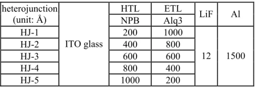
In our experiments, we fabricated OLEDs with bilayer and MH structures with the total organic thickness fixed at 120 nm which is sandwiched between ITO substrate anode and LiF (12Å)/Al (1500Å) cathode. Five HJ devices are fabricated with varying HTL and ETL thickness. The HTL thickness varies from 200Å to 1000Å, step 200Å, while the ETL thickness varies from 1000Å to 200Å in order to keep the total organic thickness 1200Å. As for the mixed layer devices, we deposite 200Å HTL followed by 800Å mixed layer. Three mixed ratios are varied with the ratio HTL: ETL=1:3, 1:1, and 3:1, respectively. After the co-deposition of the mixed layer region, 200Å ETL is deposited on it and LiF (12Å)/Al (1500Å) serves as cathode. The HTL material used in this experimental is N, N-Bis(naphthalen-1-yl)-N,N-bis(phenyl) benzidine (NPB) and the ETL material is tris(8-hydroxy-quinoline) aluminum (Alq3). The device structures and materials used are shown in Fig. 1 and Table I.
N N
Alq3
N,N -Bis(naphthalen-1-yl)-N,N -bis(phenyl) benzidine tris(8-hydroxy-quinoline) aluminum
O Al N O N O N NPB Alq3 5.4 eV 5.8 eV 2.4 eV 3.0 eV 5.0 eV 3.1 eV ITO Al
Fig. 1 Molecular structure of NPB and Alq3 and their energy diagram. NPB
3. RESULTS AND DISCUSSIONS
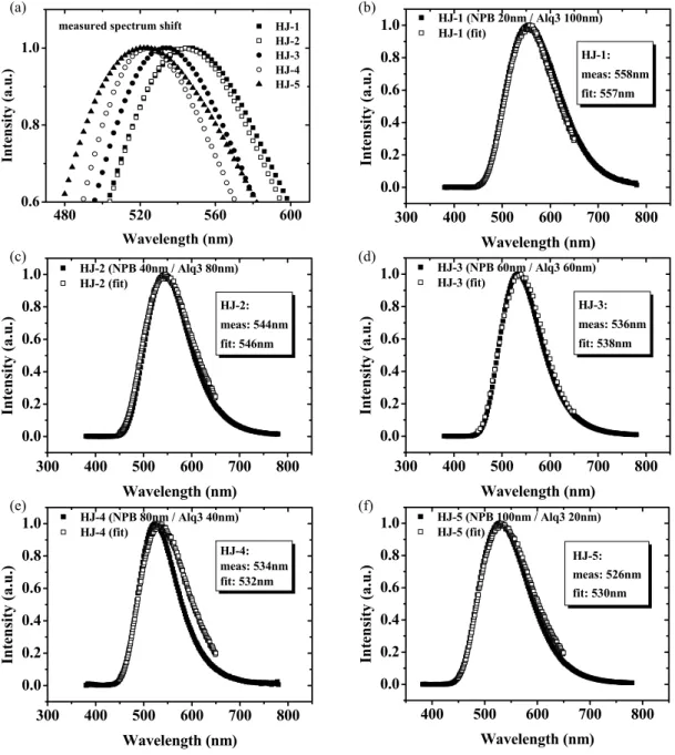
In order to identify the major recombination position of electron and hole carriers in the MH devices, first we may observe the emission spectra of the HJ devices whose total organic layer thicknesses are fixed and the HTL and ETL thicknesses vary. Figure 2 shows the measured and calculated spectra of the HJ devices. From the measured spectra data, we can see that as the HTL/ETL interface approach the metal cathode, the emission spectrum has a tendency of blue-shift. Structures of the heterojunction devices are ITO (1350Å)/ NPB (x Å) / Alq3 (1200-x Å) / LiF (12 Å) / Al (1500 Å). The EL emission spectrum peaks are 558, 544, 536, 534, 526 nm when x-value is 200, 400, 600, 800, and 1000 Å, respectively. The spectra of each HJ device at different drive voltages are almost the same and therefore we can attribute such an extensive spectra shift phenomenon of different HTL/ETL thickness device to the optical interference effect. The model of the optical interference effect in OLED can be referred to the article announced by Kahen of Eastman Kodak Company in 2001 [10]. In OLED devices, thickness of each layer is in nanometer scale and is comparable to the wavelength of light. Therefore, optical interference effect in OLED can not be neglected and must take into consideration when we analyze the device performance. Kahen presented an exact classical solution to the pattern of exciton emission in the planar multilayer OLED devices. By using this method, the color, radiative intensity, and the internal power distribution can be obtained.
The basic principle of the simulation program is based on the model established by Kahen who use Hertzian vector representation of the inhomogeneous vector wave equation as governing equation. However, we further improve the method by utilizing saddle-point method to calculate the far field electromagnetic characteristics (i.e. emitting light through a thick galss substrate) [11]. In this simulation program, we assume that electrons and holes recombine and form excitons in organic layer of the OLED device. The excitons can be represented by randomly-oriented oscillating dipoles and are imagined as an infinitive thin surface parallel to the other layer interfaces.
HTL ETL heterojunction
(unit: Å) NPB Alq3 LiF Al
HJ-1 200 1000 HJ-2 400 800 HJ-3 600 600 HJ-4 800 400 HJ-5 ITO glass 1000 200 12 1500
HTL mixed layer ETL
mixed-layer
(unit:Å) NPB NPB:Alq3 Alq3 LiF Al
ML-1 1:3 ML-2 1:1 ML-3 ITO glass 200 3:1 800 200 12 1500
Table 1 Device structures of heterojunction and mixed-layer OLEDs.
From Fig. 2 (a) we can observe that when the HTL/ETL interface approach the metal cathode, the EL spectrum shift toward short wavelength direction. Also, we can see a good agreement between the experimental results and theoretical formulation. It also confirms that the spectrum shift of different HTL/ETL layer thickness devices is caused by the optical interference effect.
The EL spectra of the MH devices are shown in Fig. 3. We can see that when NPB ratio increases, the EL spectrum blueshifts. From the point of view of optical interference effect, we may infer that the variation in EL spectrum is due to different emission dipole position in mixed layer of different mixed ratio and the blue shift in EL spectrum indicates that when NPB ratio increases, the random-oriented emission dipoles are getting closer to the metal cathode, i.e. the recombination position of holes and electrons shift toward cathode. Assuming holes and electrons hop among NPB and Alq3 molecules, respectively, in the mixed layer, the hopping distance of the holes decreases with increasing NPB concentration which makes the hole mobility gets higher. It in turns shifts the recombination zone toward the cathode and the spectrum toward shorter wavelength.
Fig. 2 (a) Measured and (b)- (f) calculated spectra of heterojunction OLEDs and their emission
300 400 500 600 700 800 0.0 0.2 0.4 0.6 0.8 1.0 HJ-1 (NPB 20nm / Alq3 100nm) HJ-1 (fit) Int ens it y (a. u .) Wavelength (nm) HJ-1: meas: 558nm fit: 557nm 300 400 500 600 700 800 0.0 0.2 0.4 0.6 0.8 1.0 HJ-2 (NPB 40nm / Alq3 80nm) HJ-2 (fit) Int ens it y (a. u .) Wavelength (nm) HJ-2: meas: 544nm fit: 546nm 300 400 500 600 700 800 0.0 0.2 0.4 0.6 0.8 1.0 HJ-3 (NPB 60nm / Alq3 60nm) HJ-3 (fit) In tens it y (a.u .) Wavelength (nm) HJ-3: meas: 536nm fit: 538nm 300 400 500 600 700 800 0.0 0.2 0.4 0.6 0.8 1.0 HJ-4 (NPB 80nm / Alq3 40nm) HJ-4 (fit) In te ns it y (a.u.) Wavelength (nm) HJ-4: meas: 534nm fit: 532nm 400 500 600 700 800 0.0 0.2 0.4 0.6 0.8 1.0 HJ-5 (NPB 100nm / Alq3 20nm) HJ-5 (fit) In te ns it y (a.u .) Wavelength (nm) HJ-5: meas: 526nm fit: 530nm 480 520 560 600 0.6 0.8 1.0 HJ-1 HJ-2 HJ-3 HJ-4 HJ-5 Intensity (a .u.) Wavelength (nm) measured spectrum shift
(a) (b)
(c) (d)
(e) (f)
Similarly, we utilized an optical simulation to fit the mixed layer EL spectra by inserting a surface of random-oriented emission dipoles at different position, step 100 Å, inside the mixed layer. In this simulation program, photoluminescence (PL) spectra and refractive index (n) and extinction coefficient (k) of each organic layer are required. Due to the solid-state salvation effect (SSSE) [12] the PL spectrum of the mixed layer has a blue shift as compared with pure Alq3 which is also shown in Fig. 3. The peak values of the PL spectra are 517, 521, 525 nm when the mixed ratios are NPB:Alq3=3:1, 1:1, and 1:3, respectively. The difference of the PL peak between pure Alq3 and NPB:Alq3=3:1 is about 9 nm. The PL spectrum of pure NPB is also shown in the Fig. 3. However, we can see that there is no NPB PL peak in the mixed films. This phenomenon can be explained by the energy transfer from NPB to Alq3 molecules. It was reported that as TPD mixed with Alq3, the fluorescence lifetime of TPD decreases when Alq3 molecules increases. The energy transfer process from TPD to Alq3 was observed to be competitive with the TPD radiation process [13]. Due to the similar molecular structure of TPD and NPB, we may adopt this concept to explain the PL spectra we measured in the experiment.
The n and k values of the thin films with different mixed ratios are shown in Fig. 4. From the figure we can see that pure NPB has largest value of refractive index and that of pure Alq3 is the smallest. At the wavelength of PL spectrum peak of Alq3, i.e. around 520nm, the n values of NPB and Alq3 are 1.82 and 1.72, respectively. The refractive index of the mixed film increases with NPB ratio. Also, we can see that when Alq3 ratio increases, the value of the relative peak shift from NPB to Alq3. The relative maximum of the refractive indices of the NPB, NPB:Alq3=3:1, 1:1, 1:3, and Alq3 are 1.96 at 392 nm, 1.91 at 400 nm, 1.88 at 412 nm, 1.87 at 418 nm, and 1.86 at 421nm, respectively. As for the extinction coefficient, there is cross-over point. When the wavelength is shorter than this cross-over point, extinction coefficient increases as NPB increases. When the wavelength is longer, extinction coefficient increases with Alq3 ratio.
The simulation results are shown in Fig. 5. By inserting emission dipole at different positions, we can estimate that the major recombination position is located inside the mixed layer away from the ITO anode about 500Å, 600Å, and 700Å for ML-1, ML-2, and ML-3, respectively. At these positions the calculated spectra have the best fit with the measured spectra. From the spectra shift we deduce the shift of the recombination zone of mixed layer with different mixed ratio, which also represents that there is a mobility variation when the mixed ratio varies. The mobility variation may reflect on the electrical properties of the devices. From the point of view of optical interference effect, we may infer that the variation in EL spectrum is due to different emission dipole position in mixed layer with different mixed ratio and the blue shift in EL spectrum indicates that when NPB ratio increases, the random-oriented emission dipoles are getting closer to the metal cathode, i.e. the recombination position of holes and electrons shift toward cathode. From this phenomenon we can verify a concept that when NPB molecules increase in the mixed layer, the hole carrier hopping distance decreases and therefore is benefit to hole current conduction, while the electrons hopping distance
400 500 600 700 800 0.0 0.2 0.4 0.6 0.8 1.0 ML-1 (NPB:Alq3=1:3) ML-2 (NPB:Alq3=1:1) ML-3 (NPB:Alq3=3:1) In te ns it y (a.u .) Wavelength (nm) 400 450 500 550 600 650 0.0 0.2 0.4 0.6 0.8 1.0 NPB NPB: Alq3=3:1 NPB: Alq3=1:1 NPB: Alq3=1:3 Alq3 In te ns it y (a.u .) Wavelength (nm)
Fig. 3 (a) EL spectra mixed layer devices and (b) PL spectra of mixed thin films.
(a) (b)
increases and lead to lower electron carrier mobility. The holes injected from HTL/mixed layer interface can propagate for a longer distance before recombination with electrons than the electrons which are injected from ETL/mixed layer interface. Therefore, the recombination position shift toward cathode as NPB ratio increases.
Fig. 4 (a) Refractive indices and (b) extinction coefficients of pure and mixed films.
AL (Cathode) 200Å Alq3 (ETL), n=nAlq3
200Å NPB (HTL), n=nNPB
1350Å ITO (Anode), n=nITO(λ)
0.7mm Glass Substrate,
100Å 800Å NPB: Alq3 (EML, mixed layer), 100Å 100Å … 400 500 600 700 800 0.0 0.2 0.4 0.6 0.8 1.0 Intensit y (a .u .) Wavelength (nm) ML-1 (NPB:Alq3=1:3) from anode 60nm from anode 50nm from anode 40nm from anode 30nm from anode 20nm 400 500 600 700 800 0.0 0.2 0.4 0.6 0.8 1.0 Intensit y (a .u. ) Wavelength (nm) ML-2 (NPB:Alq3=1:1) from anode 80nm from anode 70nm from anode 60nm from anode 50nm from anode 40nm 400 500 600 700 800 0.0 0.2 0.4 0.6 0.8 1.0 Intensit y (a .u. ) Wavelength (nm) ML-3 (NPB:Alq3=3:1) from anode 100nm from anode 90nm from anode 80nm from anode 70nm from anode 60nm
Fig. 5 (a) Schematic diagram of the simulation and (b)-(d) Calculated EL spectra of the mixed layer devices.
200 400 600 800 1000 1.6 1.7 1.8 1.9 2.0 Refr activ e inde x (n) Wavelength (nm) NPB NPB:Alq3=3:1 NPB:Alq3=1:1 NPB:Alq3=1:3 Alq3 200 400 600 800 1000 0.0 0.2 0.4 0.6 0.8 1.0 Extincti on c oefficie nt (k ) Wavelength (nm) NPB NPB:Alq3=3:1 NPB:Alq3=1:1 NPB:Alq3=1:3 Alq3 (b) (a) (a) (b) (c) (d)
4. CONCLUSIONS
In this paper we fabricated HJ and MH devices with different mixed ratios. By utilizing optical simulations, we clearly see that as NPB ratio increases, the recombination zone shifts toward metal cathode. By comparing the spectra shift between HJ and MH OLEDs, the recombination position with different mixing concentration can be determined. By fitting with an optical simulation program, we found that when the NPB:Alq3=1:3, 1:1, and 3:1, the major recombination position is away from ITO anode 500, 600, 700Å, respectively.
REFERENCES
1. Y. Shirota, Y. Kuwabara, H. lnada, T. Wakimoto, H. Nakada, Y. Yonemoto, S. Kawami, and K. lmai, Appl. Phys.
Lett., 65, 807 (1994).
2. S. A. Van Slyke, C. H. Chen, and C. W. Tang, Appl. Phys. Lett., 69, 2160 (1996).
3. Y. Hamada, T. Sano, K. Shibata, and Kazuhiko Kuroki, Jpn J. Appl. Phys., 34, L824 (1995). 4. Z. D. Popovic and H. Aziz, IEEE J. sel. top. quant. elec., 8, 362 (2002).
5. S. Naka, K. Shinno, H. Okada, H. Onnagawa, and K. Miyashita, Jpn. J. Appl. Phys., 33, L1772 (1994). 6. V. Choong, S. Shi, J. Curless, C. L. Shieh and H. C. Lee,., Appl. Phys. Lett., 75, 172 (1999).
7. A. B. Chwang, R. C. Kwong, and J. J. Brown,, Appl. Phys. Lett., 80, 725 (2002). 8. D. Ma, C. S. Lee, S. T. Lee, and L. S. Hung., Appl. Phys. Lett., 80, 3641 (2002). 9. C.C. Wu, C. I. Wu, J. C. Sturm, and A. Kahn, Appl. Phys. Lett., 70, 1348 (1997). 10. K. B. Kahen, Appl. Phys. Lett., 78, 1649 (2001).
11. H. C. Chen, J. H. Lee, Y. W. Kiang, C. C. Yang, and Yih Chang, The Fifth Pacific Rim Conference on Lasers and
Electro-Optics (CLEO/PR), Taipei, Taiwan, Dec. 2003.
12. M. A. Baldo, Z. G. Soo, and S. R. Forrest, Chem. Phys. Lett., 347, 297 (2001).
13. T. Mori, K. Obata, K. Miyachi, T. Mizutani and Y. Kawakami, Jpn. J. Appl. Phys., 36, 7239 (1997).